

Battery charger system with integrated
Features
■ Fully integrated solution, with a power
MOSFET, reverse blocking diode, sense
resistor, and thermal protection
■ Ideal for coke and graphite anode single-cell L
I
packs
ON
■ Both linear and quasi-pulse operation
■ Closed loop thermal control
■ USB BUS-compatible
■ Programmable charge current up to 1 A
■ Programmable pre-charge current
■ Programmable end-of-charge current
■ Programmable pre-charge voltage threshold
■ Programmable charge timer
■ Programmable output voltage at 4.1 V and 4.2
V, with ± 1 % output voltage accuracy
■ (NTC) or (PTC) thermistor interface for battery
temperature monitoring and protection
■ Flexible charge process termination
■ Status outputs to drive LEDs or to interface
with a host processor
■ Small VFQFPN 16-leads package (3 x 3 mm)
L6924D
power switch for Li-Ion/Li-Polymer
-
I
VFQFPN16
Applications
■ PDAs
■ Handheld devices
■ Cellular phones
■ Digital cameras
■ Standalone chargers
■ USB-powered chargers
Table 1. Device summary
Order code Package Packaging
L6924D
VFQFPN16
L6924D013TR Tape and reel
September 2010 Doc ID 11908 Rev 9 1/38
Tube
www.st.com
38

Contents L6924D
Contents
1 Description . . . . . . . . . . . . . . . . . . . . . . . . . . . . . . . . . . . . . . . . . . . . . . . . . 3
2 Pins description and connection diagrams . . . . . . . . . . . . . . . . . . . . . . 4
2.1 Pin description . . . . . . . . . . . . . . . . . . . . . . . . . . . . . . . . . . . . . . . . . . . . . . 4
3 Maximum ratings . . . . . . . . . . . . . . . . . . . . . . . . . . . . . . . . . . . . . . . . . . . . 6
3.1 Absolute maximum ratings . . . . . . . . . . . . . . . . . . . . . . . . . . . . . . . . . . . . . 6
3.2 Thermal data . . . . . . . . . . . . . . . . . . . . . . . . . . . . . . . . . . . . . . . . . . . . . . . 6
4 Electrical specifications . . . . . . . . . . . . . . . . . . . . . . . . . . . . . . . . . . . . . . 7
4.1 Electrical characteristics . . . . . . . . . . . . . . . . . . . . . . . . . . . . . . . . . . . . . . . 7
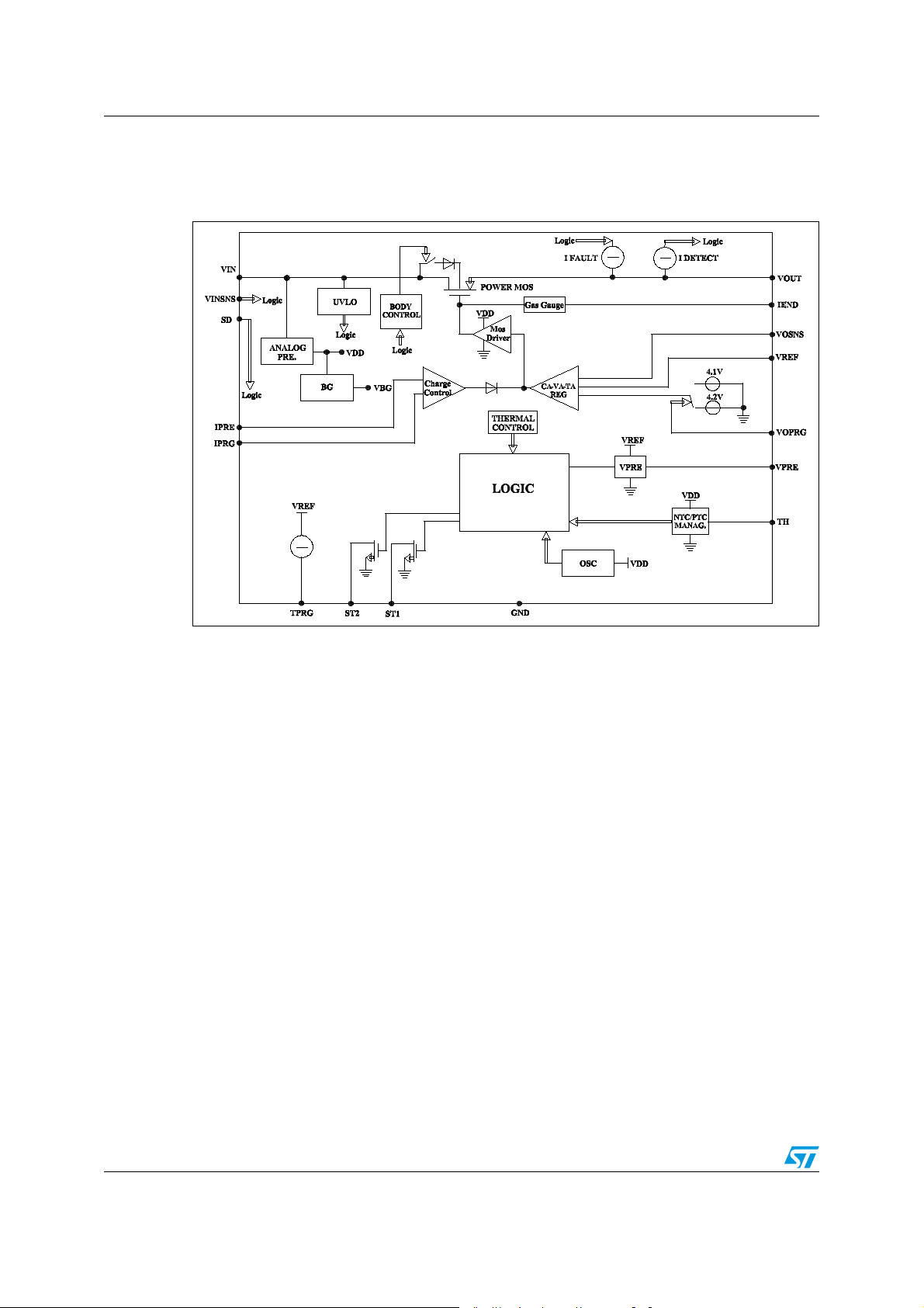
5 Block diagram . . . . . . . . . . . . . . . . . . . . . . . . . . . . . . . . . . . . . . . . . . . . . . 9
6 Operation description . . . . . . . . . . . . . . . . . . . . . . . . . . . . . . . . . . . . . . . 10
6.1 Linear mode . . . . . . . . . . . . . . . . . . . . . . . . . . . . . . . . . . . . . . . . . . . . . . . 11
6.2 Quasi-pulse mode . . . . . . . . . . . . . . . . . . . . . . . . . . . . . . . . . . . . . . . . . . 13
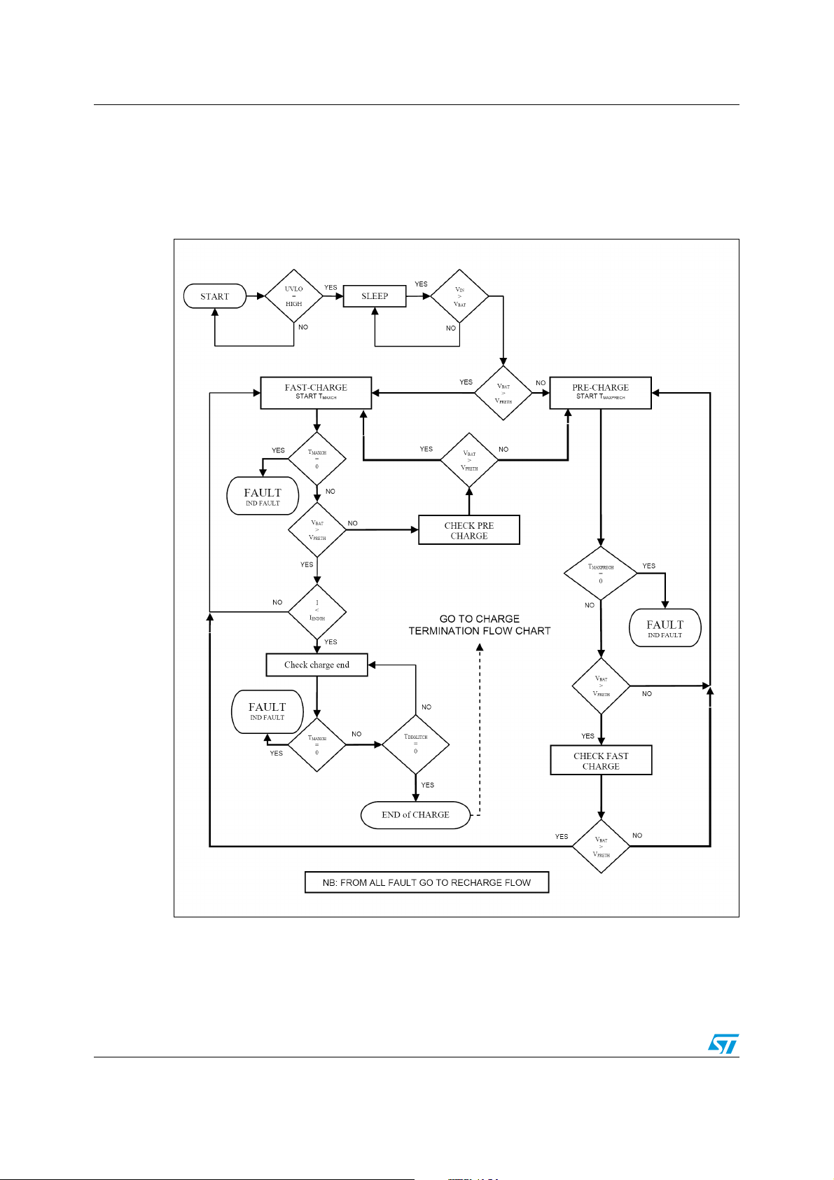
7 Applications information: charging process . . . . . . . . . . . . . . . . . . . . 16
7.1 Charging process flow chart . . . . . . . . . . . . . . . . . . . . . . . . . . . . . . . . . . . 16
7.2 Pre-charge current . . . . . . . . . . . . . . . . . . . . . . . . . . . . . . . . . . . . . . . . . . 17
7.3 Pre-charge voltage . . . . . . . . . . . . . . . . . . . . . . . . . . . . . . . . . . . . . . . . . . 17
7.4 Fast charge current . . . . . . . . . . . . . . . . . . . . . . . . . . . . . . . . . . . . . . . . . 18
7.5 End-of-charge current . . . . . . . . . . . . . . . . . . . . . . . . . . . . . . . . . . . . . . . 19
7.6 Recharge flow chart . . . . . . . . . . . . . . . . . . . . . . . . . . . . . . . . . . . . . . . . . 20
7.7 Recharge threshold . . . . . . . . . . . . . . . . . . . . . . . . . . . . . . . . . . . . . . . . . 20
7.8 Maximum charging time . . . . . . . . . . . . . . . . . . . . . . . . . . . . . . . . . . . . . . 20
7.9 Termination modes . . . . . . . . . . . . . . . . . . . . . . . . . . . . . . . . . . . . . . . . . . 22
8 Application information: monitoring and protection . . . . . . . . . . . . . . 23
8.1 NTC thermistor . . . . . . . . . . . . . . . . . . . . . . . . . . . . . . . . . . . . . . . . . . . . . 23
8.2 Battery absence detection . . . . . . . . . . . . . . . . . . . . . . . . . . . . . . . . . . . . 27
8.3 Status pins . . . . . . . . . . . . . . . . . . . . . . . . . . . . . . . . . . . . . . . . . . . . . . . . 27
2/38 Doc ID 11908 Rev 9

L6924D Contents
8.4 Shutdown . . . . . . . . . . . . . . . . . . . . . . . . . . . . . . . . . . . . . . . . . . . . . . . . . 28
9 Additional applications information . . . . . . . . . . . . . . . . . . . . . . . . . . . 30
9.1 Selecting the input capacitor . . . . . . . . . . . . . . . . . . . . . . . . . . . . . . . . . . 30
9.2 Selecting the output capacitor . . . . . . . . . . . . . . . . . . . . . . . . . . . . . . . . . 30
9.3 Layout guidelines and demonstration board description . . . . . . . . . . . . . 30
10 Application ideas . . . . . . . . . . . . . . . . . . . . . . . . . . . . . . . . . . . . . . . . . . . 34
10.1 USB battery charger . . . . . . . . . . . . . . . . . . . . . . . . . . . . . . . . . . . . . . . . . 34
11 Package mechanical data . . . . . . . . . . . . . . . . . . . . . . . . . . . . . . . . . . . . 35
12 Revision history . . . . . . . . . . . . . . . . . . . . . . . . . . . . . . . . . . . . . . . . . . . 37
Doc ID 11908 Rev 9 3/38
Description L6924D
1 Description
The L6924D is a fully monolithic battery charger dedicated to single-cell Li-Ion/Polymer
battery packs. It is the ideal solution for space-limited applications, like PDAs, handheld
equipment, cellular phones, and digital cameras. It integrates all of the power elements (the
power MOSFET, reverse blocking diode and the sense resistor) in a small VFQFPN16 (3 x 3
mm) package. When an external voltage regulated wall adapter is used, the L6924D works
in Linear Mode, and charges the battery in a constant current/constant voltage (CC/CV)
profile. Moreover, when a current-limited adapter is used, the device can operate in quasipulse mode, dramatically reducing the power dissipation. Regardless of the charging
approach, a closed loop thermal control avoids device overheating. The device has an
operating input voltage ranging from 2.5 V to 12 V. The L6924D allows the user to program
many parameters, such as pre-charge current, fast-charge current, pre-charge voltage
threshold, end-of-charge current threshold, and charge timer. The L6924D offers two open
collector outputs for diagnostic purposes, which can be used to either drive two external
LEDs or communicate with a host microcontroller. Finally, the L6924D also provides very
flexible control of the charge process termination and Gas Gauge capability, as well as other
functions, such as checking for battery presence, and monitoring and protecting the battery
from unsafe thermal conditions.
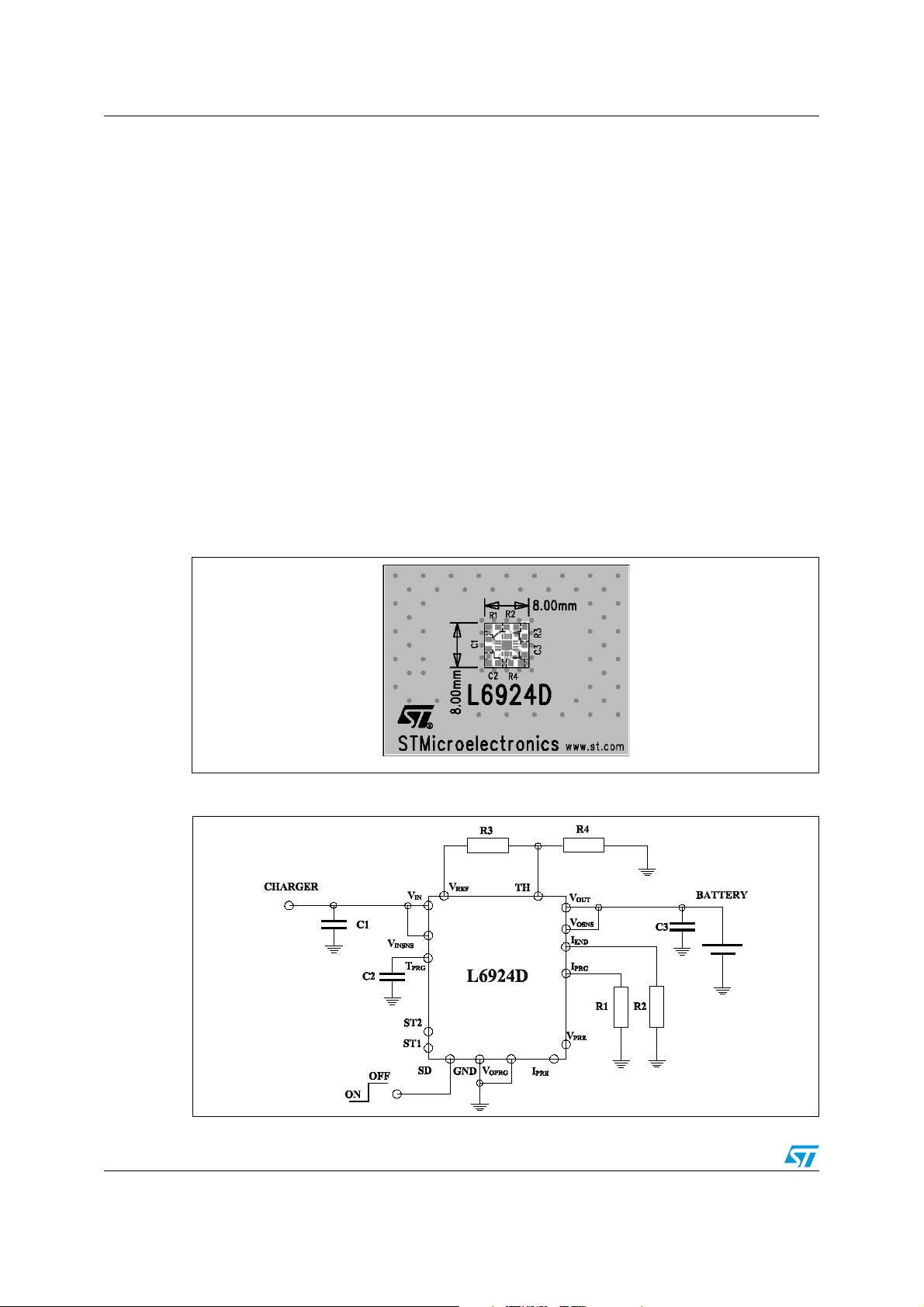
Figure 1. Minimum application size
Figure 2. Basis application schematic
4/38 Doc ID 11908 Rev 9
L6924D Pins description and connection diagrams
2 Pins description and connection diagrams
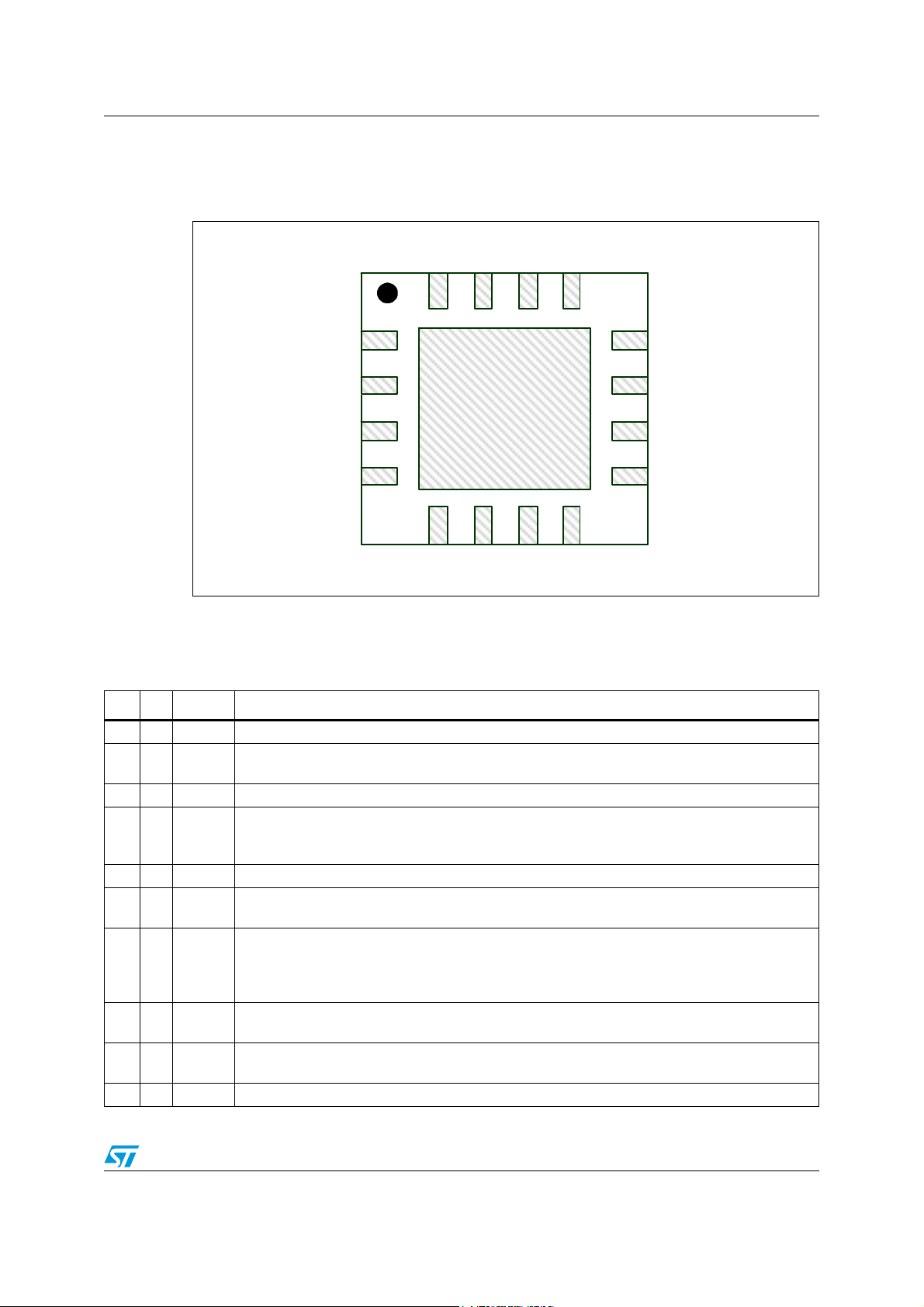
Figure 3. Pins connection (top view)
I
PRG
V
PRE
V
V
INSNS
IN
I
PRE
ST2
ST1
T
PRG
GND SD
2.1 Pin description
Table 2. Pin functions
Pin I/O Name Pin description
1I V
2IV
3-4 O ST
5IT
6 - GND Ground pin.
7I SD
8I TH
9IV
10 I V
11 O V
INSNS
OPRG
OSNS
Input pin of the power stage.
IN
Supply voltage pin of the signal circuitry.
The operating input voltage ranges from 2.5 V to 12 V and the start-up threshold is 4 V.
-ST1Open-collector status pins.
2
Maximum charging time program pin.
It must be connected with a capacitor to GND to fix the maximum charging time, see
PRG
Chapter 7.8: Maximum charging time on page 20
Shutdown pin.
When connected to GND enables the device; when floating disables the device.
Temperature monitor pin.
It must be connected to a resistor divider including an NTC or PTC resistor. The charge
process is disabled if the battery temperature (sensed through the NTC or PTC) is out of the
programmable temperature window see Chapter 8.1: NTC thermistor on page 23.
Output voltage selection pin.
V
= 4.1 V if left floating. V
OUT
Output voltage sense pin.
It senses the battery voltage to control the voltage regulation loop.
Output pin. (connected to the battery)
OUT
= 4.2 V if connected to GND.
OUT
I
I
END
END
TH
V
REF
V
OUT
V
V
OSNS
OSNS
V
OPRG
Doc ID 11908 Rev 9 5/38

Pins description and connection diagrams L6924D
Table 2. Pin functions
12 O V
13 I/O I
14 I V
15 I I
16 I I
External reference voltage pin.(reference voltage is 1.8 V±2%)
REF
Charge termination pin.
A resistor connected from this pin to GND fixes the charge termination current threshold
END
I
ENDTH
: if I < I
, the charger behaves according to the V
ENDTH
status (see Chapter 7.5:
PRE
End-of-charge current on page 19). The voltage across the resistor is proportional to the
current delivered to the battery (Gas Gauge function).
Multifunction pin.
A resistor connected to GND allows the user to adjust the pre-charge voltage threshold
PRETH
.
= 2.8 V. If the voltage on V
PRETH
goes lower than 0.5 V (edge sensitive), the maximum charging time is
PRE
pin is lower than 0.8 V, V
PRE
ENDTH
.
V
If the pin is floating, V
PRE
2.8 V and the charge is not automatically terminated when I < I
If the voltage on V
reset.
Charge current program pin.
A resistor connected from this pin to GND, fixes the fast charge current value (I
PRG
accuracy of 7%.
Pre-charge current program pin.
If the pin is floating I
PRE
different value, the pin has to be connected to GND or V
is equal to 10% of I
PRETH
CHG
. If I
has to be programmed at a
PRETH
,
through a resistor see
REF
Chapter 7.2: Pre-charge current on page 17.
CHG
=
PRETH
), with an
6/38 Doc ID 11908 Rev 9
L6924D Maximum ratings
3 Maximum ratings
Stressing the device above the rating listed in the “absolute maximum ratings” table may
cause permanent damage to the device. These are stress ratings only and operation of the
device at these or any other conditions above those indicated in the operating sections of
this specification is not implied. Exposure to absolute maximum rating conditions for
extended periods may affect device reliability.
3.1 Absolute maximum ratings
Table 3. Absolute maximum ratings
Symbol Parameter Value Unit
V
IN
, SD Input voltage –0.3 to V
V
INSNS
V
, V
OUT
OSNS
ST1, ST2
V
REF
V
PRE
, TH, I
, I
T
PRG
PRE
END
, V
, GND
, I
PRG
OPRG
ST1 and TH pins Maximum withstanding voltage range test condition:
Other pins ±2 kV
3.2 Thermal data
Table 4. Thermal data
Symbol Parameter Value Unit
R
thJA
T
STG
T
J
P
TOT
1. Device mounted on demonstration board
Input voltage –0.3 to 16 V
IN
Output voltage –0.3 to 5 V
Output voltage –0.3 to 6 V
Output current 30 mA
,
,
–0.3 to 4 V
±1.5 kV
CDFAEC-Q100-002 (Normal “human body model”
acceptance criteria performance)
Thermal resistance junction to ambient
(1)
75 °C/W
Storage temperature range –55 to 150 °C
Junction temperature range –40 to 125 °C
Power dissipation at T= 70 °C TBD W
V
Doc ID 11908 Rev 9 7/38

Electrical specifications L6924D
4 Electrical specifications
4.1 Electrical characteristics
TJ = 25 °C, V
Table 5. Electrical characteristics
= 5 V, unless otherwise specified.
IN
Symbol Parameter Test condition Min Typ Max Unit
Operating input voltage 2.5 12 V
(1)
V
IN
I
IN
I
SINK
V
OUT
I
CHG
I
PRECH
I
PRECH
I
PRECH
V
PRETH
V
PRETH
Start up threshold 4.1 V
(1)
Supply current
Current flowing from V
(1)
Battery regulated voltage
OUT
Charge current
Pre-Charge current
[default value = 10% I
CHG
Pre-Charge current
Pre-Charge current
Pre-Charge voltage threshold
[default]
Pre-Charge voltage threshold R
Charging mode (R
Shutdown mode (R
Shutdown mode (R
Stand by mode (R
= 2.5V < V
(V
IN
V
at V
OPRG
V
OPRG
R
PRG
R
PRG
I
PRE
]
R
PRG
R
PRE
R
PRG
R
PRE
R
PRG
V
PRE
VPRE
IN
at GND 4.16 4.2 4.24 V
= 24kΩ 450 490 525 mA
= 12kΩ 905 975 1045 mA
floating
= 24kΩ
= 62kΩ to GND;
= 24kΩ
= 39kΩ to V
= 24kΩ
= V
PRETHDefault
= 13kΩ; R
= 24kΩ)1.82.5mA
PRG
= 24kΩ)6080µA
PRG
= 24kΩ)500nA
PRG
= 24kΩ)
PRG
BATTERY
)
4.06 4.1 4.14 V
41 49 56 mA
57 67 78 mA
;
REF
29.5 35 40.1 mA
= Floating 2.7 2.8 2.9 V
= 12kΩ 2.87 3.03 3.19 V
PRG
500 nA
Pre-Charge voltage threshold
V
PRETH
[default]. Charge termination
2.7 2.8 2.9 V
disabled
I
ENDTH
T
MAXCH
T
MAXCH
(2)
Termination current R
(2)
Maximum charging time
Maximum charging time accuracy
= 3K3 12 16 20 mA
END
C
= 10nF
TPRG
R[I
C
TPRG
R
PRG
PRG
= 24kΩ
] = 24kΩ
= 5.6nF
3 hours
10%
Shutdown threshold high 2 V
SD
TH
Shutdown threshold low 0.4 V
ST1,2 Output status sink current Status on 10 mA
R
DS(on)
Power MOSFET resistance R
DS(on)@ICHG
= 500mA 280 380 mΩ
8/38 Doc ID 11908 Rev 9

L6924D Electrical specifications
Table 5. Electrical characteristics (continued)
Symbol Parameter Test condition Min Typ Max Unit
TH
NTC pin hot threshold voltage 10.625 12.5 14.375 %V
NTC pin cold threshold voltage 45 50 55 %V
1. TJ from –40°C to 125°C.
2. Guaranteed by design.
REF
REF
Doc ID 11908 Rev 9 9/38
Block diagram L6924D
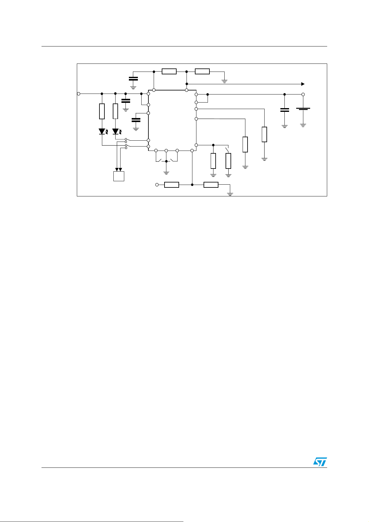
5 Block diagram
Figure 4. Block diagram
10/38 Doc ID 11908 Rev 9

L6924D Operation description
6 Operation description
The L6924D is a fully integrated battery charger that allows a very compact battery
management system for space limited applications. It integrates in a small package, all the
power elements: power MOSFET, reverse blocking diode and the sense resistor.
It normally works as a linear charger when powered from an external voltage regulated
adapter. However, thanks to its very low minimum input voltage (down to 2.5 V) the L6924D
can also work as a Quasi-Pulse charger when powered from a current limited adapter. To
work in this condition, is enough to set the device’s charging current higher than the
adapter’s one (Chapter 7.4 on page 18). The advantage of the linear charging approach is
that the device has a direct control of the charging current and so the designer needn’t to
rely on the upstream adapter. However, the advantage of the Quasi-Pulse approach is that
the power dissipated inside the portable equipment is dramatically reduced.
The L6924D charges the battery in three phases:
● Pre-Charge constant current: in this phase (active when the battery is deeply
discharged) the battery is charged with a low current.
● Fast-Charge constant current: in this phase the device charges the battery with the
maximum current.
● Constant Voltage: when the battery voltage reaches the selected output voltage, the
device starts to reduce the current, until the charge termination is done.
The full flexibility is provided by:
● Programmable pre-charging current and voltage thresholds (I
PRETH
and V
PRETH
)
(Chapter 7.2 on page 17, Chapter 7.3 on page 17).
● Programmable fast-charging current (I
● Programmable end of charge current threshold (I
● Programmable end of charge timer (T
) (Chapter 7.4 on page 18).
CHG
) (Chapter 7.5 on page 19).
ENDTH
) (Chapter 7.8 on page 20).
MAXCH
If the full flexibility is not required and a smaller number of external components is preferred,
default values of I
● If a PTC or NTC resistor is used, the device can monitor the battery temperature in
PRETH
and V
are available leaving the respective pins floating.
PRETH
order to protect the battery from operating in unsafe thermal conditions.
● Beside the good thermal behavior guaranteed by low thermal resistance of the
package, additional safety is provided by the built-in temperature control loop. The IC
monitors continuously its junction temperature. When the temperature reaches
approximately 120°C, the thermal control loop starts working, and reduces the charging
current, in order to keep the IC junction temperature at 120°C.
● Two open collector outputs are available for diagnostic purpose (status pins ST1 and
ST2). They can be also used to drive external LEDs or to interface with a
microcontroller.
The voltage across the resistor connected between I
and GND gives information about
END
the actual charging current (working as a Gas Gauge), and it can be easily fed into a µC
ADC.
Doc ID 11908 Rev 9 11/38
Operation description L6924D
When the V
pin is not used to program the Pre-Charge voltage threshold, it has two
PRE
different functions:
● If the voltage across V
pin is lower than 0.8 V, when I < I
PRE
, the end of charge is
ENDTH
notified by the status pin, but the charging process is not disabled. The charge process
ends when the maximum charging time expires.
● If the voltage at V
pin false under 0.5 V the timer is reset on the falling edge.
PRE
Battery disconnection control is provided thanks to the differentiated sensing and forcing
output pins. A small current is sunk and forced through V
OUT
. If V
doesn’t detect the
OSNS
battery, the IC goes into a standby mode.
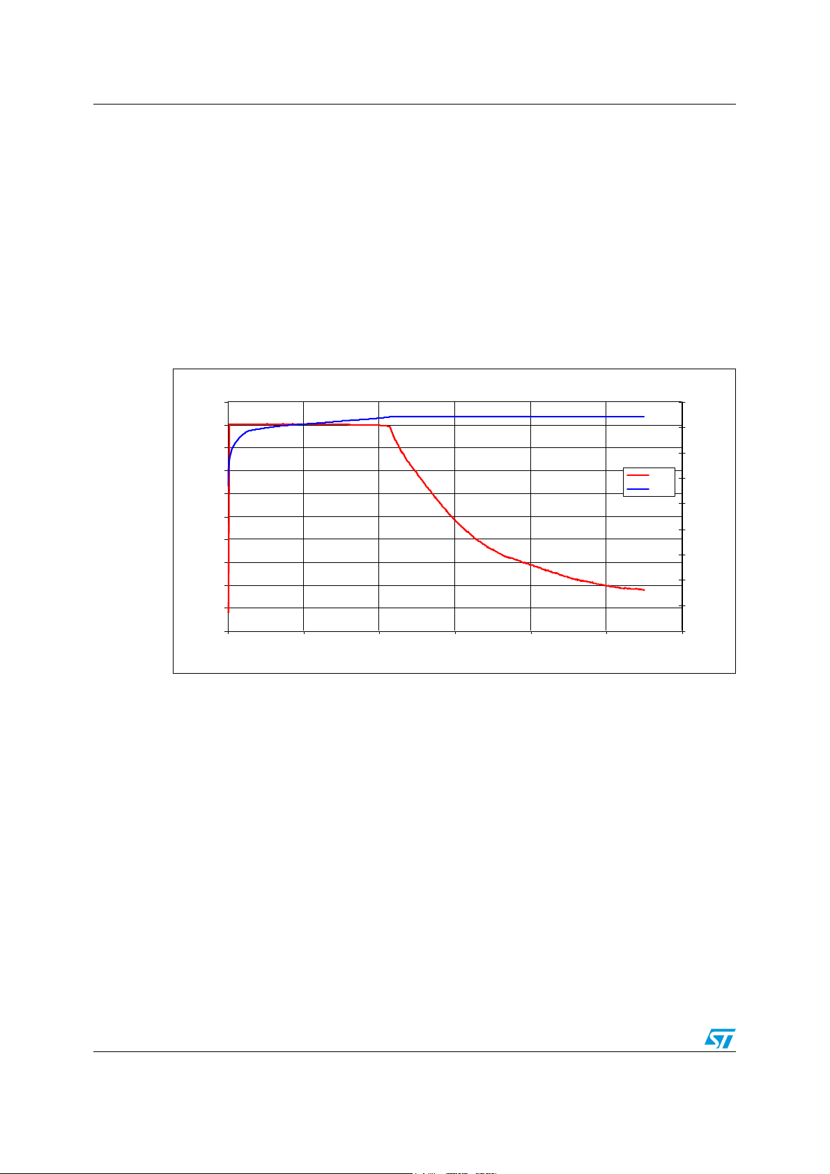
Figure 5 shows the real charging profile of a Li-Ion battery, with a fast charge current of 450
mA (R
PRG
= 26 kΩ),
Figure 5. Li-Ion charging profile
Charging profile
Ich g
Vb a tt
4.500
4.000
3.500
3.000
2.500
2.000
1.500
1.000
0.500
0.000
0.500
0.450
0.400
0.350
0.300
0.250
Ichg (A )
0.200
0.150
0.100
0.050
0.000
0 200 400 600 800 1000 1200
Charging time (sec)
Vbatt (V)
6.1 Linear mode
When operating in linear mode, the device works in a way similar to a linear regulator with a
constant current limit protection.
It charges the battery in three phases:
● Pre-charging current (“Pre-Charge” phase).
● Constant current (“Fast-Charge” phase).
● Constant voltage (“Voltage Regulation” phase).
V
is the output voltage of the upstream AC-DC adapter that is, in turn, the input voltage
ADP
of the L6924D. If the battery voltage is lower than a set pre-charge voltage (V
pre-charge phase takes place. The battery is pre-charged with a low current I
(Chapter 7.2 on page 17).
When the battery voltage goes higher than V
charge current I
, set through an external resistor (Chapter 7.4 on page 18).
CHG
Finally, when the battery voltage is close to the regulated output voltage V
4.2 V), the voltage regulation phase takes place and the charging current is reduced. The
12/38 Doc ID 11908 Rev 9
PRETH
), the
PRETH
PRE
, the battery is charged with the fast
OPRGTH
(4.1 V or

L6924D Operation description
×−=
charging process is usually terminated when the charging current reaches a set value or
when a charging timer expires (Chapter 7.9 on page 22).
Figure 6 shows the different phases.
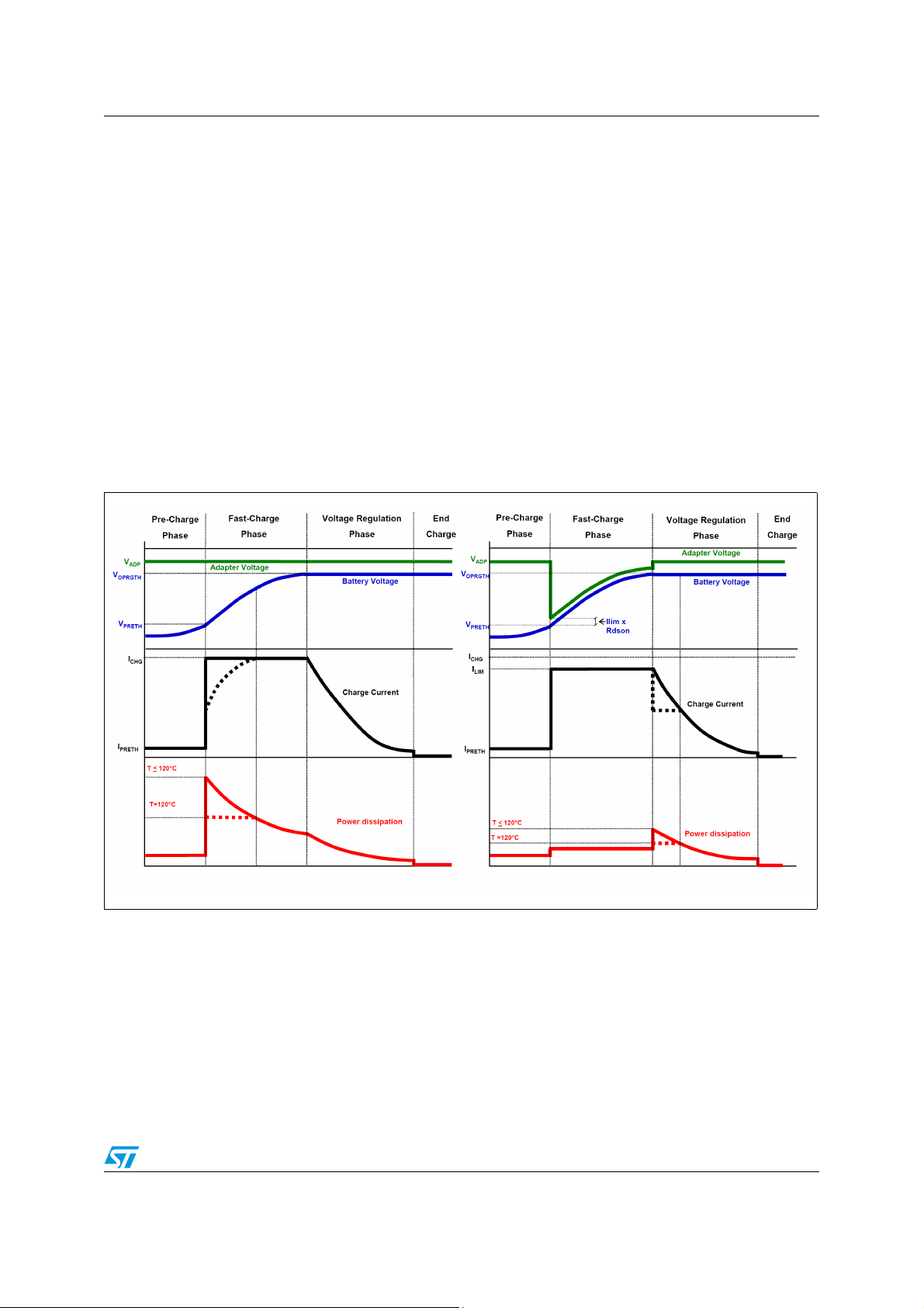
Figure 6. Typical charge curves in linear mode
V
OPRGTH
V
I
V
ADP
PRETH
I
CHG
PRETH
Pre-Charge
Phase
Fast-Charge
Phase
Adapter Voltage
Voltage-Regulation
Phase
Battery Voltage
Charge Current
Power dissipation
End
Charge
The worst case in power dissipation occurs when the device starts the fast-charge phase. In
fact, the battery voltage is at its minimum value. In this case, this is the maximum difference
between the adapter voltage and battery voltage, and the charge current is at its maximum
value.
The power dissipated is given by the following equation:
Equation 1
IVVP
)(
CHGBATADPDIS
The higher the adapter voltage is, the higher the power dissipated. The maximum power
dissipated depends on the thermal impedance of the device mounted on board.
Doc ID 11908 Rev 9 13/38

Operation description L6924D
Δ+=
=
Δ
6.2 Quasi-pulse mode
The quasi-pulse mode can be used when the system can rely on the current limit of the
upstream adapter to charge the battery. In this case, I
current limit of the adapter. In this mode, the L6924D charges the battery with the same
three phases as in linear mode, but the power dissipation is greatly reduced as shown in
Figure 7.
Figure 7. Typical charge curves in quasi pulse mode
must be set higher than the
CHG
V
OPRGTH
V
I
V
ADP
PRETH
I
CHG
I
LIM
PRETH
Pre-Charge
Phase
Fast-Charge
Phase
Ilim x R dson
Voltage Regulation
Phase
Adapter Voltage
Battery Voltage
Charge Current
End
Charge
The big difference is due to the fact that I
is higher than the current limit of the adapter.
CHG
During the fast-charge phase, the output voltage of the adapter drops and goes down to the
battery voltage plus the voltage drop across the power MOSFET of the charger, as shown in
the following equation:
Equation 2
Where ΔV
is given by:
MOS
Equation 3
V
MOS
14/38 Doc ID 11908 Rev 9
Power dissipation
VVVV
MOSBATADPIN
×=
IR
LIMONDS
)(

L6924D Operation description
×−=
Where,
I
= current limit of the wall adapter, and R
LIM
= resistance of the power MOSFET.
DS(on)
The difference between the set charge current and the adapter limit should be high enough
to minimize the R
value (and the power dissipation). This makes the control loop
DS(on)
completely unbalanced and the power element is fully turned on.
Figure 8 shows the R
values for different output voltage and charging currents for an
DS(on)
adapter current limit of 500 mA.
Figure 8. R
curves vs charging current and output voltage
DS(on)
Neglecting the voltage drop across the charger (ΔV
) when the device operates in this
MOS
condition, its input voltage is equal to the battery one, and so a very low operating input
voltage (down to 2.5 V) is required. The power dissipated by the device during this phase is:
Equation 4
2
IRP ×=
)( LIMonDSCH
When the battery voltage approaches the final value, the charger gets back the control of
the current, reducing it. Due to this, the upstream adapter exits the current limit condition
and its output goes up to the regulated voltage V
. This is the worst case in power
ADP
dissipation:
Equation 5
IVVP
)(
LIMBATADPDIS
In conclusion, the advantage of the linear charging approach is that the designer has the
direct control of the charge current, and consequently the application can be very simple.
The drawback is the high power dissipation.
The advantage of the Quasi-Pulse charging method is that the power dissipated is
dramatically reduced. The drawback is that a dedicated upstream adapter is required.
Doc ID 11908 Rev 9 15/38
Applications information: charging process L6924D
7 Applications information: charging process
7.1 Charging process flow chart
Figure 9. Charging process flow chart
16/38 Doc ID 11908 Rev 9
L6924D Applications information: charging process
−
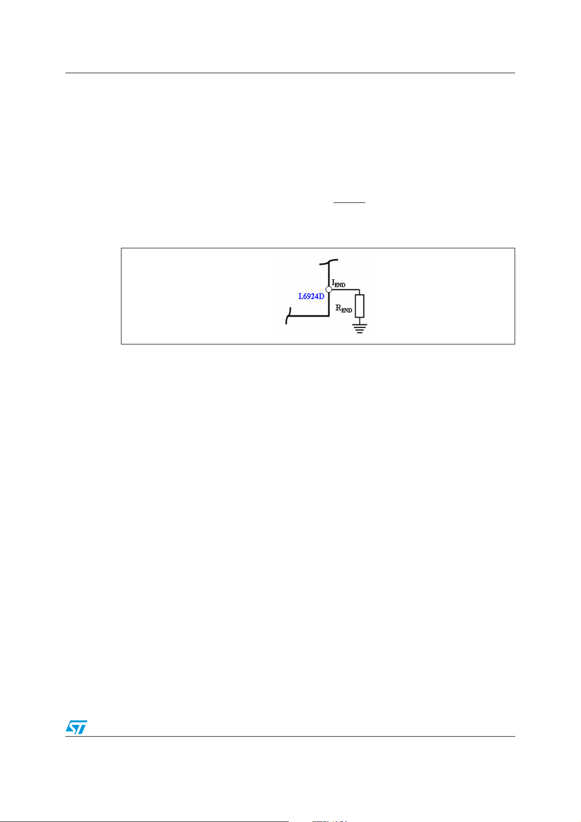
7.2 Pre-charge current
The L6924D allows pre-charging the battery with a low current when the battery voltage is
lower than a specified threshold (V
to 10% of the fast-charge current. However it can be adjusted by connecting a resistor from
the I
pin to GND or V
PRE
(see Figure 10). When the resistor is connected between I
REF
pin and GND, the current is higher than the default value. The R
Equation 6
). The Pre-charge current has a default value equal
PRETH
value is given by:
PRE
V
R−=
PRE
I
PRECH
K
PRE
BG
V
BG
R
PRG
PRE
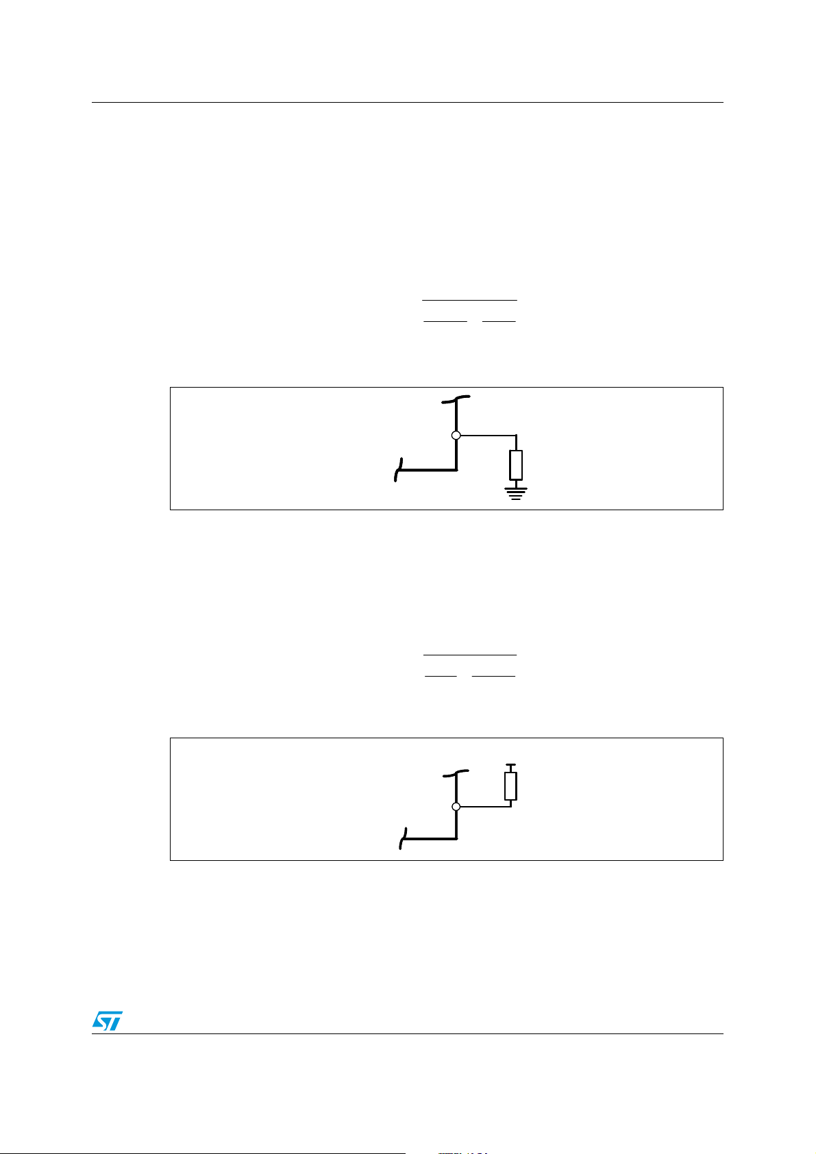
Figure 10. I
When R
PRE
external reference equal to 1.8 V, V
pin connection
PRE
is connected to V
L6924D
L6924D
, the current is lower than the default value. V
REF
is the internal reference equal to 1.23 V and K
BG
constant equal to 950. See Figure 11.
The relationship is shown in the equation 7:
Equation 7
=
PRE
R
Figure 11. I
pin connection
PRE
I
I
PRE
PRE
is the
REF
BG
VV
REF
I
BG
V
PRG
R
PRECH
−
PRE
K
V
V
REF
REF
PRE
is a
I
I
PRE
PRE
L6924D
L6924D
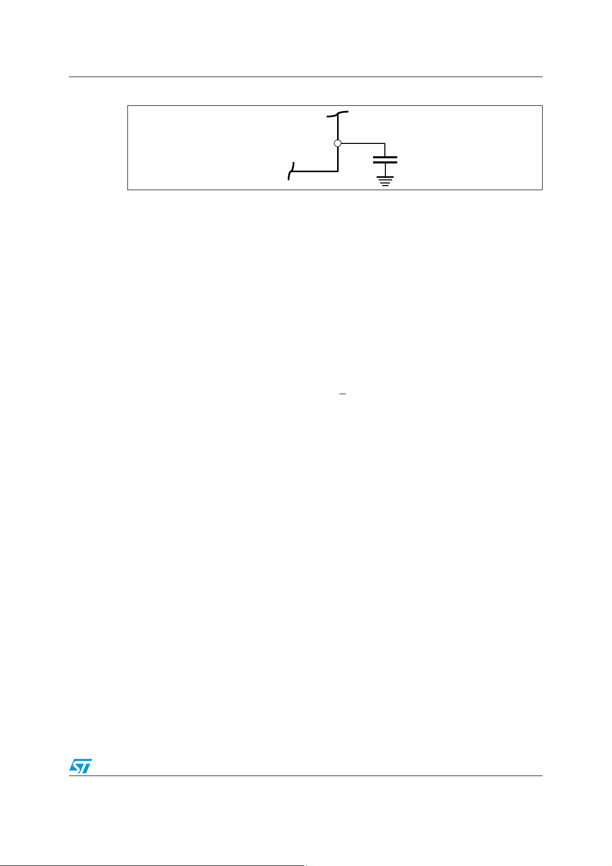
7.3 Pre-charge voltage
If the V
Otherwise, the device offers the possibility to program this value, with a resistor connected
between the V
equation 8:
pin is floating, a default value of V
PRE
pin and GND (see Figure 12). In this case, the R
PRE
Doc ID 11908 Rev 9 17/38
is set, equal to 2.8 V (V
PRETH
PRETHDefault
is given by the
VPRE
).

Applications information: charging process L6924D
Equation 8
Figure 12. V
Where R
VPRE
pin connection
PRE
is the resistor between V
the charge current (see Section 7.4: Fast charge current), and V
threshold.
A safety timer is also present. If the battery voltage doesn't rise over V
time is expired, a fault is given (see Section 7.8: Maximum charging time). If at the beginning
of the charge process, the battery voltage is higher than the V
is skipped.
7.4 Fast charge current
⎛
RR
L6924D
L6924D
PRE
⎜
×=
PRGVPRE
⎜
V
⎝
V
V
and GND, and R
PRE
PRE
V
R
R
PRETH
PRE
PRE
⎞
⎟
⎟
ltPRETHDefau
⎠
is the resistor used to set
PRG
PRETH
is the selected
PRETH
, before this
PRETH
, the Pre-Charge phase
When the battery voltage reaches the Pre-charge voltage threshold (V
), the L6924D
PRETH
starts the Fast-charge Phase. In this phase, the device charges the battery with a constant
current, I
accuracy of 7% Figure 13. The equation used to select the R
, programmable by an external resistor that sets the charge current with an
CHG
as follows:
PRG
Equation 9
K
I
PRG
CHG
⎞
⎟
⎟
⎠
Figure 13. I
Where K
PRG
pin connection
PRG
is a constant, equal to 9500.
⎛
⎜
BGPRG
VR
×=
⎜
⎝
During this phase, the battery voltage increases until it reaches the programmed output
voltage. A safety timer is also present. If this time expires, a fault is given (Section 7.8:
Maximum charging time).
18/38 Doc ID 11908 Rev 9
L6924D Applications information: charging process
7.5 End-of-charge current
When the charge voltage approaches the selected value (4.1 V or 4.2 V), the voltage
regulation phase takes place. The charge current starts to decrease until it goes lower than
a programmable end value, I
the I
Equation 10
pin and GND (see Figure 14). The equation that describes this relation as follows:
END
, depending on an external resistor connected between
ENDTH
END
K
ENDTH
⎞
⎟
⎟
⎠
is
END
⎛
⎜
MINEND
VR
×=
⎜
I
⎝
Figure 14. I
Where K
Typically, this current level is used to terminate the charge process. However, it is also
possible to disable the charge termination process based on this current level (Chapter 7.9
on page 22).
This pin is also used to monitor the charge current, because the current injected in R
proportional to I
charge status like a gas gauge.
END
pin connection
END
is 1050; and V
. The voltage across R
CHG
is 50 mV.
MIN
can be used by a microcontroller to check the
END
Doc ID 11908 Rev 9 19/38
Applications information: charging process L6924D
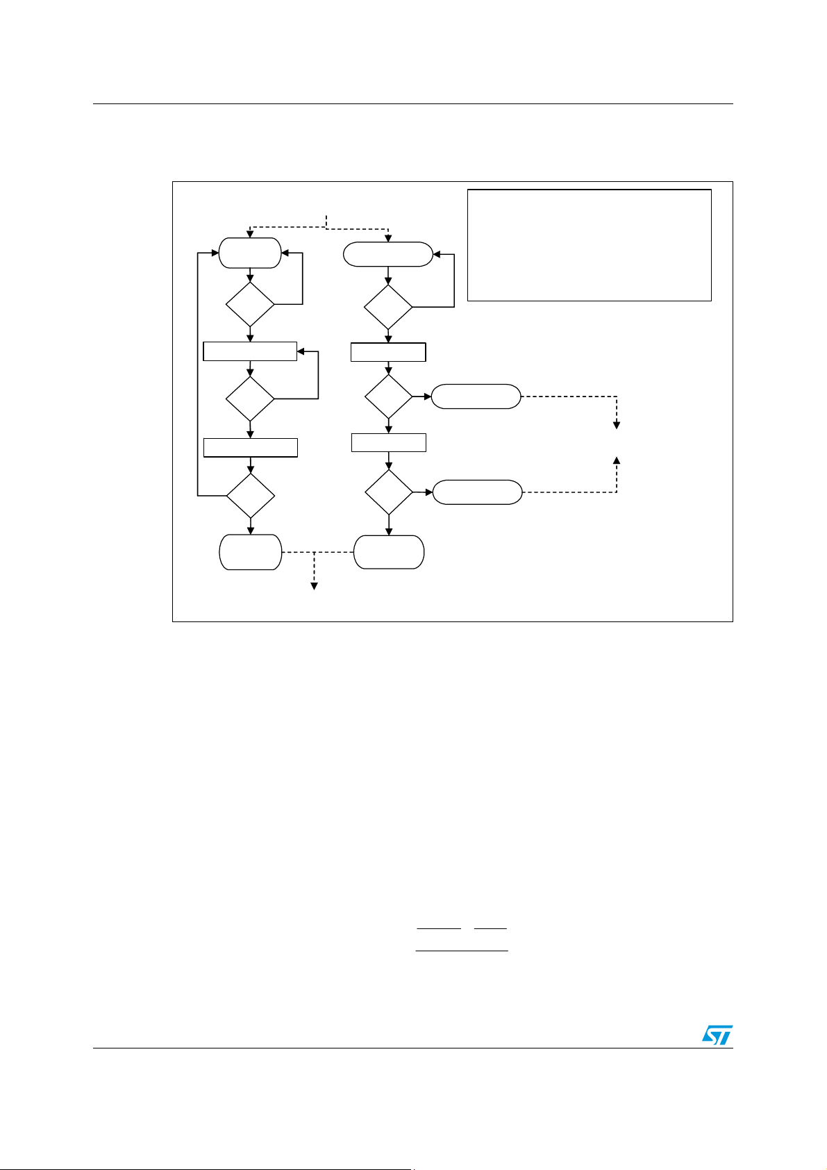
7.6 Recharge flow chart
Figure 15. Recharge flow chart
FROM CHARGING PROCESS FLOW CHART
FAULT
IND FAULT
V
YES
BAT
>
V
RCH
NO
Detect High Fault
V
BAT
YES
<
V
ABS
NO
Detect Low Fault
YES
V
BAT
>
V
PRETH
NO
BATTERY
ABSENT
GO TO BATTERY ABSENT
FLOW CHART
END of CHARGE
V
BAT
>
V
RCH
NO
Detect Low
V
BAT
>
V
PRETH
NO
Detect High
V
BAT
>
V
RCH
NO
BATTERY
ABSENT
YES
YES
YES
DETECT LOW = a I
DETECT HIGH = a I
DETECT LOW FAULT = a I
DETECT HIGH FAULT = a I
V
= V
ABS
OPRG
= V
V
RCH
OPRG
T
= 100ms (Typ.)
DET
I
= I
= 1mA (Typ.)
SINK
INJ
FAST CHARGE
PRE CHARGE
is sunk for a T
SINK
is injected for a T
INJ
– 50mV
– 150mV
RETURN TO CHARGING PROCESS
DET
is sunk for a T
SINK
is injected for a T
INJ
FLOW CHART
from the battery
in the battery
DET
from the battery
DET
in the battery
DET
7.7 Recharge threshold
When, from an end-of-charge condition, the battery voltage goes lower than the recharging
threshold (V
threshold is V
), the device goes back in charging state. The value of the recharge
RCH
OPRG
–150 mV.
7.8 Maximum charging time
To avoid the charging of a dead battery for a long time, the L6924D has the possibility to set
a maximum charging time starting from the beginning of the fast-charge phase. This timer
can be set with a capacitor, connected between the T
external capacitor (in nF) and is given by the following equation:
Equation 11
⎛
T
MAXCH
⎜
K
T
C
Note: The maximum recommended C
20/38 Doc ID 11908 Rev 9
TPRG
⎜
=
TPRG
⎜
V
⎜
⎝
REF
value must be less than 50 nF.
pin and GND. The C
PRG
⎞
V
BG
×
⎟
R
PRG
⎟
9
10×
⎟
⎟
⎠
TPRG
is the
L6924D Applications information: charging process
Figure 16. T
pin connection
PRG
L6924D
T
PRG
C
TPRG
Where,
= 1.8V,
V
REF
K
= 279 x 105,
T
V
= 1.23V, and
BG
T
is the charging time given in seconds.
MAXCH
If the battery does not reach the end-of-charge condition before the timer expires, a fault is
issued.
Also during the pre-charge phase there is a safety timer, given by:
Equation 12
1
TT ×=
MAXCHMAXPRECH
8
If this timer expires and the battery voltage is still lower than V
generated, and the charge process is terminated.
, a fault signal is
PRETH
Doc ID 11908 Rev 9 21/38
Applications information: charging process L6924D
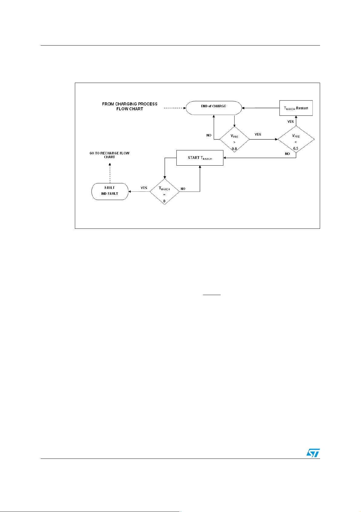
7.9 Termination modes
Figure 17. Charge termination flow chart
As shown in Figure 14, it is possible to set an end of charge current I
resistor between the I
pin and GND. When the charge current goes down to this value,
END
ENDTH
connecting a
after a de-glitch time, the status pins notify that the charge process is complete. This deglitch time is expressed as:
Equation 13
T
T =
DEGLITCH
However, the termination of the charger process depends on the status of the V
● If the voltage at the V
pin is higher than 0.8 V, the charge process is actually
PRE
terminated when the charge current reaches I
● If the voltage at V
pin goes lower than 0.8 V, the charge process does not terminate,
PRE
and the charge current can go lower than I
charge as a fault condition, but the device continues the charge. When the T
MAXCH
220
.
ENDTH
. The status pins notify the end-of-
ENDTH
PRE
MAXCH
pin:
elapsed, the charge process ends, and a fault condition is issued.
● If the voltage on V
sets the V
● If the voltage at the V
PRETHDefault
pin is lower than 0.8 V during the Pre-charge Phase, the device
PRE
automatically.
pin goes lower than 0.5 V (edge sensitive), the timer is reset,
PRE
both in pre-charge and in fast-charge phase.
is
22/38 Doc ID 11908 Rev 9
L6924D Application information: monitoring and protection
8 Application information: monitoring and protection
The L6924D uses a VFQFPN 3 mm x 3 mm 16-pin package with an exposed pad that
allows the user to have a compact application and good thermal behavior at the same time.
The L6924D has a low thermal resistance because of the exposed pad (approximately
75°C/W, depending on the board characteristics). Moreover, a built-in thermal protection
feature prevents the L6924D from having thermal issues typically present in a linear charger.
Thermal control is implemented with a thermal loop that reduces the charge current
automatically when the junction temperature reaches approximately 120 °C. This avoids
further temperature rise and keeps the junction temperature constant. This simplifies the
thermal design of the application as well as protects the device against over-temperature
damage.
The Figure 18 shows how the thermal loop acts (with the dotted lines), when the junction
temperature reaches 120°C.
Figure 18. Power dissipation both linear and quasi pulse mode with thermal loop
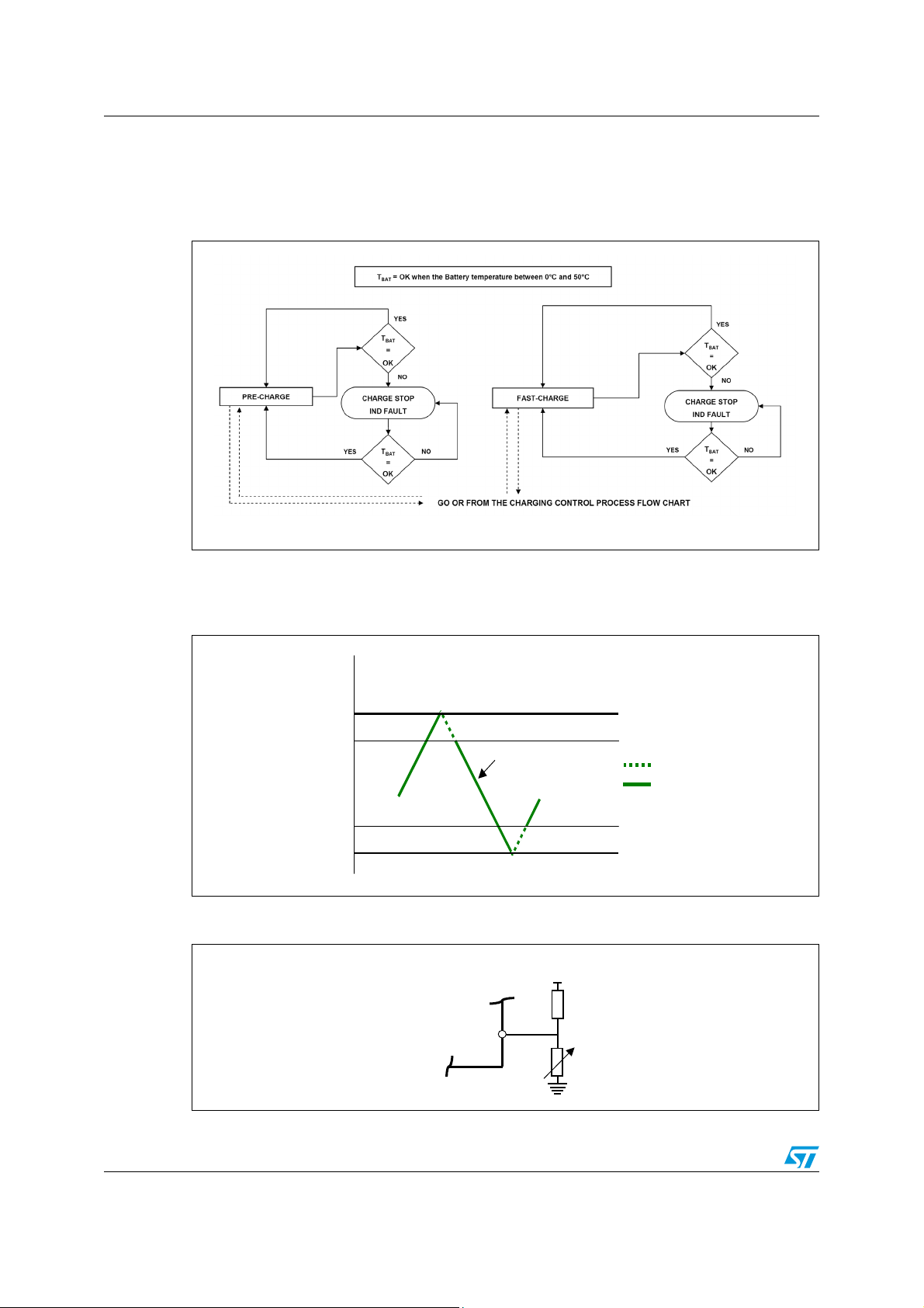
8.1 NTC thermistor
The device allows designers to monitor the battery temperature by measuring the voltage
across an NTC or PTC resistor. Li-Ion batteries have a narrow range of operating
temperature, usually from 0°C to 50 °C. This window is programmable by an external divider
which is comprised of an NTC thermistor connected to GND and a resistor connected to
V
. When the voltage on the TH pin exceeds the minimum or maximum voltage threshold
REF
(internal window comparator), the device stops the charge process, and indicates a fault
condition through the status pin.
Doc ID 11908 Rev 9 23/38
Application information: monitoring and protection L6924D
When the voltage (and thus, the temperature), returns to the window range, the device restarts the charging process. Moreover, there is a hysteresis for both the upper and lower
thresholds, as shown in Figure 20.
Figure 19. Battery temperature control flow chart
Note: T
= OK when the battery temperature between 0°C and 50°C
BAT
Figure 20. Voltage window with hysteresis on TH
V
MI N T H
V
MINTH_ HYS
900mV
780mV
Vol t ag e
Vari atio n on TH pi n
V
MAXTH_HYS
V
MAXTH
248mV
225mV
Figure 21. Pin connection
V
TH
L6924D
NTC
Charge disable
Charge enable
REF
24/38 Doc ID 11908 Rev 9

L6924D Application information: monitoring and protection
=
When the TH pin voltage rises and exceeds the V
MINTH
= 50% of V
(900 mV typ), the
REF
L6924D stops the charge, and indicates a fault by the status pins. The device re-starts to
charge the battery, only when the voltage at the TH pin goes under V
MINTH_HYS
= 780 mV
(typ).
For what concerns the high temperature limit, when the TH pin voltage falls under the
V
MAXTH
voltage rises to the V
= 12.5% of V
(225 mV Typ.), the L6924D stops the charge until the TH pin
REF
MAXTH_HYS
= 248 mV (Typ.).
When the battery is at the low temperature limit, the TH pin voltage is 900 mV. The correct
resistance ratio to set the low temperature limit at 0°C can be found with the following
equation:
Equation 14
R
CNTC
°
VV
×=
REFMINTH
Where R
is the pull-up resistor, V
UP
is equal to 1.8 V, and R
REF
NTC at 0°C. Since at the low temperature limit V
+
MINTH
0
RR
CNTCUP
°
0
= 900 mV:
is the value of the
NTC0°C
Equation 15
R
CNTC
°
8.19.0
×=
0
RR
+
CNTCUP
°
0
It follows that:
Equation 16
RR
UPCNTC
°0
Similarly, when the battery is at the high temperature limit, the TH pin voltage is 225 mV. The
correct resistance ratio to set the high temperature limit at 50°C can be found with the
following equation:
Equation 17
Where R
NTC50°C
VV
REFMAXTH
R
×=
is the value of the NTC at 50°C. Considering V
CNTC
°
50
RR
+
CNTCUP
°
50
= 225 mV it follows
MAXTH
that:
Equation 18
8.1225.0
R
×=
CNTC
°
50
RR
+
CNTCUP
°
50
Consequently:
Equation 19
R =
Doc ID 11908 Rev 9 25/38
R
50UPCNTC
°
7

Application information: monitoring and protection L6924D
−
−
−
−
−
Based on Equation 16: and Equation 19: , it derives that:
Equation 20
R
0
CNTC
7
R
=
50
°°CNTC
The temperature hysteresis can be estimated by the equation:
Equation 21
VV
HYSTHTH
=
T
HYS
_
NTCV
×
TTH
Where V
threshold on the falling edge, and NTC
the NTC at temperature (T) expressed in % resistance change per °C. For NTC
is the pin voltage threshold on the rising edge, V
TH
(-%/°C) is the negative temperature coefficient of
T
TH_HYS
is the pin voltage
values, see
T
the characteristics of the NTC manufacturers (e.g. the 2322615 series by VISHAY). At the
low temperature, the hysteresis is approximately:
Equation 22
mVmV
T
=
CHYS
°
0
780900
CNTCmV
°×
0900
Obviously at the high temperature hysteresis is:
Equation 23
mVmV
T
Considering typical values for NTC
CHYS
°
50
and NTC
0°C
=
248225
CNTCmV
°×
50225
, the hysteresis is:
50°C
Equation 24
mVmV
T
=
CHYS
0
°
mV
780900
051.0900
×
o
C
5.2
≅
And:
Equation 25
mVmV
T
=
CHYS
50
°
mV
248225
039.0225
×
o
C
5.2
−≅
If a PTC connected to GND is used, the selection is the same as above, the only difference
is when the battery temperature increases, the voltage on the TH pin increases, and vice
versa. For applications that do not need a monitor of the battery temperature, the NTC can
be replaced with a simple resistor whose value is one half of the pull-up resistor R
UP
.
In this case, the voltage at the TH pin is always inside the voltage window, and the charge is
always enabled.
26/38 Doc ID 11908 Rev 9

L6924D Application information: monitoring and protection
8.2 Battery absence detection
This feature provides a battery absent detection scheme to detect the removal or the
insertion of the battery. If the battery is removed, the charge current falls below the I
At the end of the de-glitch time, a detection current I
output for a time of T
V
, a current equal to I
PRETH
DETECT
. The device checks the voltage at the output. If it is below the
DETECT
is injected in the output capacitor for a T
DETECT
checked to see if the voltage on the output goes higher than V
mV). If the battery voltage changes from V
PRETH
to V
it means that no battery is connected to the charger. The T
, equal to 1 mA, is sunk from the
(the value is V
ABS
and vice versa in a T
ABS
DETECT
is expressed by:
DETECT
Equation 26
T
MAXCH
T
DETECT
=
3
1054 ×
Figure 22. Battery absent detection flow chart
, and it is
OPRGTH
DETECT
ENDTH
-50
time,
.
Detect Low Absent
Detect High Absent
YES
BATTERY
ABSENT
V
BAT
>
V
PRETH
NO
V
BAT
>
V
RCH
YES
NO
DETECT LOW ABSENT = a I
DETECT HIGH ABSENT = a I
= 100ms (Typ.)
T
DET
= I
I
SINK
= 1mA (Typ.)
INJ
FAST CHARGE
PRE CHARGE
is sunk for a T
SINK
is injected for a T
INJ
from the battery
DET
in the battery
DET
8.3 Status pins
To indicate various charger status conditions, there are two open-collector output pins, ST1
and ST2. These status pins can be used either to drive status LEDs, connected to an
external power source, by a resistor, or to communicate to a host processor. These pins
must never be connected to the V
when it exceeds their absolute value (6 V).
IN
Doc ID 11908 Rev 9 27/38

Application information: monitoring and protection L6924D
Figure 23. ST1 and ST2 connection with LEDs or microcontroller
Table 6. Status LEDs indications
Charge condition Description ST1 ST2
Charge in progress When the device is in pre-charge or fast-charge status ON OFF
Charge done When the charging current goes lower than the I
Stand by mode When the input voltage goes under V
Bad battery temperature
Battery absent When the battery pack is removed ON ON
Over time When T
8.4 Shutdown
The L6924D has a shutdown pin (SD) that allows enabling or disabling the device.
If the SD pin voltage is below 0.4 V (e.g. pin connected to GND), the device is enabled,
whereas if the SD pin voltage exceeds 2 V (e.g. the shutdown pin is left floating) the device
is disabled.
When the device enters the shutdown mode, the current consumption is reduced to 60 μA
typ. In this condition, V
The Figure 24 clarifies the SD pin behavior.
ENDTH
-50 mV OFF OFF
BAT
When the voltage on the TH pin is out of the programmable
window, in accordance with the NTC or PTC thermistor
is turned off.
REF
MAXCH
or T
MAXPRECH
is expired ON ON
OFF ON
ON ON
28/38 Doc ID 11908 Rev 9

L6924D Application information: monitoring and protection
Figure 24. Shutdown
SD
SD
pin voltage
pin voltage
device disabled
device disabled
2V
2V
0.4V
0.4V
device enabled
device enabled
SD
SD
SD
SD
TH,high
TH,high
TH,low
TH,low
Doc ID 11908 Rev 9 29/38

Additional applications information L6924D
+×=
9 Additional applications information
9.1 Selecting the input capacitor
In most applications, a 1 µF ceramic capacitor, placed close to the VIN and V
be used to filter the high frequency noise.
INSN
pins can
9.2 Selecting the output capacitor
Typically, 1 µF ceramic capacitor placed close to the V
keep voltage control loop stable. This ensures proper operation of battery absent detection
in removable battery pack applications.
OUT
and V
pin is enough to
OUTSN
9.3 Layout guidelines and demonstration board description
The thermal loop keeps the device at a constant temperature of approximately 120°C which
in turn, reduces I
ensure a good thermal path. Therefore, the exposed pad must be properly soldered to the
board and connected to the other layer through thermal vias. The recommended copper
thickness of the layers is 70 µm or more.
The exposed pad must be electrically connected to GND. Figure 25 shows the thermal
image of the board with the power dissipation of 1 W. In this instance, the temperature of the
case is 89°C, but the junction temperature of the device is given by the following equation:
Equation 27
. However, in order to maximize the current capability, it is important to
CHG
TPRT
−
AMBDISSATHJJ
Where the R
and the ambient temperature is 25 °C.
In this case the junction temperature is:
Equation 28
30/38 Doc ID 11908 Rev 9
of the device mounted on board is 75 °C/W, the power dissipated is 1 W,
TH J-A
J
o
CT
10025175 =+×=

L6924D Additional applications information
Figure 25. Thermal image of the demonstration board
The V
pin can be used as a remote sense; it should be therefore connected as closely
OSNS
as possible to the battery. The demonstration board layout and schematic are shown in
Figure 26, Figure 27 and Figure 28.
Figure 26. Demonstration board layout, top side
Figure 27. Demonstration board layout, bottom side
Doc ID 11908 Rev 9 31/38
Additional applications information L6924D
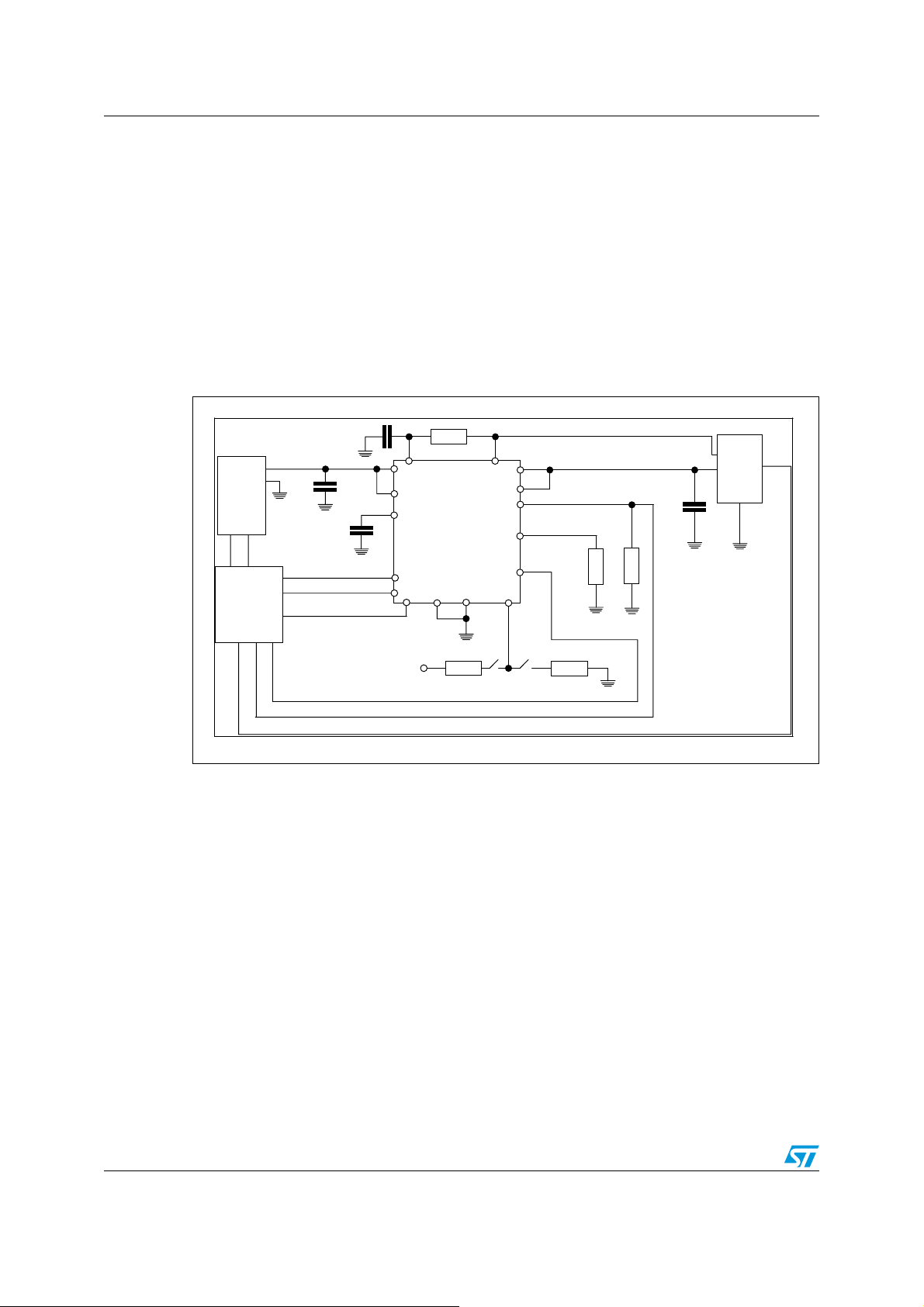
Figure 28. Demonstration board schematic
R9
V
OUT
V
OSNS
I
END
I
PRG
V
PRE
I
PRE
CHARGER
R1 R2
LD1 LD2
μC
R3
C4
V
REF
V
IN
TH
C1
V
INSNS
T
PRG
C2
J2
ST2
L6924D
ST1
J1
SHDN
GND
J3
V
OPRG
J4
Vref
R7
NTC
BATTERY
C3
R4
R5
J5
R6
R10
R8
32/38 Doc ID 11908 Rev 9

L6924D Additional applications information
Table 7. Demonstration board components description
Name Value Description
R1 1k Pull up resistor. To be used when the ST1 is connected to a LED.
R2 1k Pull up resistor. To be used when the ST1 is connected to a LED.
R3 1k Pull up resistor. Connected between V
R4 3k3
End of charge current resistor. Used to set the termination current and, as a “Gas
Gauge” when measuring the voltage across on it.
and TH pin.
REF
R5 24k Fast-charge current resistor. Used to set the charging current.
R6 N.M.
R7 N.M.
R8 68k
R9 470R
R10 N.M.
V
mounted, the V
I
the default one. If not mounted, the I
I
the default one. If not mounted, the I
If a NTC is not used, a half value of R3 must be mounted to keep the TH voltage in
the correct window.
It has the same function of R6. Moreover, if it is replaced with a short-circuit, when
J5 is closed, the timer is reset (falling edge).
resistor. Used to set programmable pre-charge voltage threshold. If not
PRETH
PRETHDefault
resistor. Used to set the programmable pre-charge current threshold below
PRETH
resistor. Used to set the programmable pre-charge current threshold above
PRETH
, equal to 2.8V, is set.
PRETHDefault
PRETHDefault
is set.
is set.
C1 1µF Input capacitor.
C2 10nF T
capacitor. Used to set the maximum charging time.
MAX
C3 4.7µF Output capacitor.
C4 1nF V
filter capacitor.
REF
LD1 GREEN ST1 LED.
LD2 RED ST2 LED.
J1 ST1 jumper. Using to select the LED or the external µC.
J2 ST2 jumper. Using to select the LED or the external µC.
J3
J4 V
J5 V
SD jumper. If open, the device is in shutdown mode; when closed, the device starts
to work.
jumper. If closed, the 4.2V output voltage is set; if open, the 4.1V is set.
OPRG
jumper. If closed with R10 in short-circuit with GND, resets the timer.
PRE
Doc ID 11908 Rev 9 33/38
Application ideas L6924D
10 Application ideas
10.1 USB battery charger
With a voltage range between 4.75 V and 5.25 V, and a maximum current up to 500 mA, the
USB power bus is an ideal source for charging a single-cell Li-Ion battery. Since it is not
possible to rely on the USB current limit to charge the battery, a linear approach must be
adopted. Therefore, it is only necessary to set the I
500 mA, and the device will charge the battery in Linear mode.
Figure 29 shows an example of USB charger application schematic.
Figure 29. USB charger application
with a maximum value lower than
CHG
V
BUS
GND
D- D+
SYSTEM
AND
USB
CONTROLLER
V
V
T
ST1
ST2
IN
INSNS
PRG
R1
V
REF
L6924D
GND
SD
TH
V
OUT
V
OSNS
I
END
I
PRG
V
PRE
I
V
PRE
OPRG
R4
R2 R3
R5
C3
BATTERY
PACK
C4
C1
C2
34/38 Doc ID 11908 Rev 9

L6924D Package mechanical data
11 Package mechanical data
In order to meet environmental requirements, ST offers these devices in different grades of
ECOPACK
specifications, grade definitions and product status are available at: www.st.com.
ECOPACK
®
packages, depending on their level of environmental compliance. ECOPACK®
®
is an ST trademark.
Doc ID 11908 Rev 9 35/38
Package mechanical data L6924D
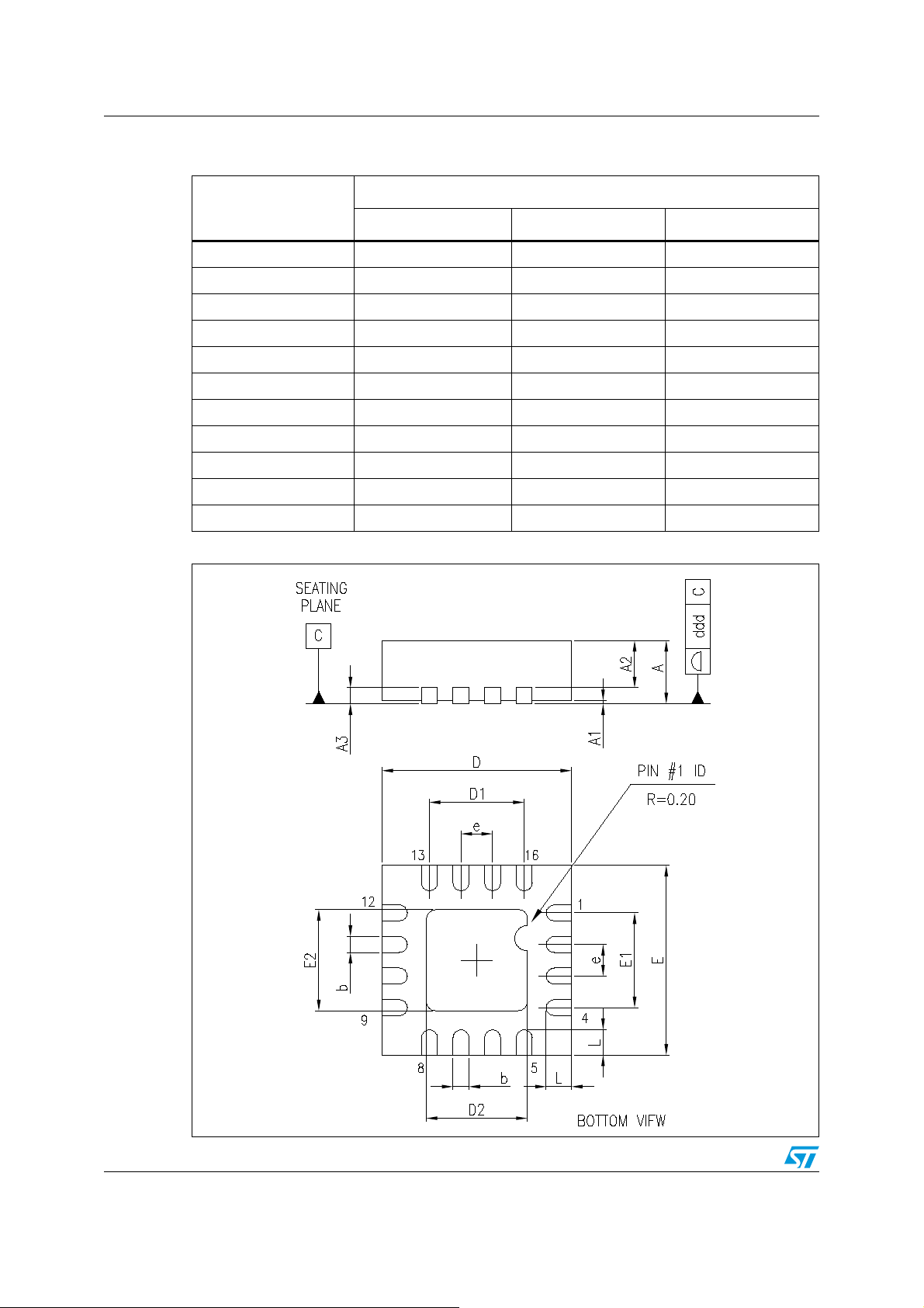
Table 8. VFQFPN16 (3 x 3 mm.) mechanical data
mm.
Dim.
Min. Typ. Max.
A 0.80 0.90 1.00
A1 0.02 0.05
A2 0.65 1.00
A3 0.20
b 0.18 0.25 0.30
D 2.85 3.00 3.15
D2 1.45 1.60 1.75
E 2.85 3.00 3.15
E2 1.45 1.60 1.75
e 0.45 0.50 0.55
L 0.30 0.40 0.50
Figure 30. Package dimensions
36/38 Doc ID 11908 Rev 9
7185330_G

L6924D Revision history
12 Revision history
Table 9. Document revision history
Date Revision Changes
16-Dec-2005 1 First draft
20-Dec-2005 2 Package dimensions updated
10-Jan-2006 3 Few updates
14-Feb-2006 4 Part number updated
03-Jul-2006 5 Updates to equation in page 22, updated block diagram Figure 4.
07-Sep-2006 6 Added Note: on page 20, updated value C
29-Jun-2007 7 Updated capacitor values C2, C3 in Table 7 on page 33
05-Jul-2010 8 Updated Table 5 on page 8 and Section 8.4 on page 28
22-Sep-2010 9 Updated Ta b le 8 and Figure 30 on page 36. Minor changes.
TPRG
page 8
Doc ID 11908 Rev 9 37/38

L6924D
Please Read Carefully:
Information in this document is provided solely in connection with ST products. STMicroelectronics NV and its subsidiaries (“ST”) reserve the
right to make changes, corrections, modifications or improvements, to this document, and the products and services described herein at any
time, without notice.
All ST products are sold pursuant to ST’s terms and conditions of sale.
Purchasers are solely responsible for the choice, selection and use of the ST products and services described herein, and ST assumes no
liability whatsoever relating to the choice, selection or use of the ST products and services described herein.
No license, express or implied, by estoppel or otherwise, to any intellectual property rights is granted under this document. If any part of this
document refers to any third party products or services it shall not be deemed a license grant by ST for the use of such third party products
or services, or any intellectual property contained therein or considered as a warranty covering the use in any manner whatsoever of such
third party products or services or any intellectual property contained therein.
UNLESS OTHERWISE SET FORTH IN ST’S TERMS AND CONDITIONS OF SALE ST DISCLAIMS ANY EXPRESS OR IMPLIED
WARRANTY WITH RESPECT TO THE USE AND/OR SALE OF ST PRODUCTS INCLUDING WITHOUT LIMITATION IMPLIED
WARRANTIES OF MERCHANTABILITY, FITNESS FOR A PARTICULAR PURPOSE (AND THEIR EQUIVALENTS UNDER THE LAWS
OF ANY JURISDICTION), OR INFRINGEMENT OF ANY PATENT, COPYRIGHT OR OTHER INTELLECTUAL PROPERTY RIGHT.
UNLESS EXPRESSLY APPROVED IN WRITING BY AN AUTHORIZED ST REPRESENTATIVE, ST PRODUCTS ARE NOT
RECOMMENDED, AUTHORIZED OR WARRANTED FOR USE IN MILITARY, AIR CRAFT, SPACE, LIFE SAVING, OR LIFE SUSTAINING
APPLICATIONS, NOR IN PRODUCTS OR SYSTEMS WHERE FAILURE OR MALFUNCTION MAY RESULT IN PERSONAL INJURY,
DEATH, OR SEVERE PROPERTY OR ENVIRONMENTAL DAMAGE. ST PRODUCTS WHICH ARE NOT SPECIFIED AS "AUTOMOTIVE
GRADE" MAY ONLY BE USED IN AUTOMOTIVE APPLICATIONS AT USER’S OWN RISK.
Resale of ST products with provisions different from the statements and/or technical features set forth in this document shall immediately void
any warranty granted by ST for the ST product or service described herein and shall not create or extend in any manner whatsoever, any
liability of ST.
ST and the ST logo are trademarks or registered trademarks of ST in various countries.
Information in this document supersedes and replaces all information previously supplied.
The ST logo is a registered trademark of STMicroelectronics. All other names are the property of their respective owners.
© 2010 STMicroelectronics - All rights reserved
STMicroelectronics group of companies
Australia - Belgium - Brazil - Canada - China - Czech Republic - Finland - France - Germany - Hong Kong - India - Israel - Italy - Japan -
Malaysia - Malta - Morocco - Philippines - Singapore - Spain - Sweden - Switzerland - United Kingdom - United States of America
www.st.com
38/38 Doc ID 11908 Rev 9
 Loading...