


L6920
Fi
1V HIGH EFFICIENCY SYNCRONOUS STEP UP CONVERTER
1 Features
■ 0.6 TO 5.5V OPERATING INPUT VOLTAGE
■ 1V START UP INPUT VOLTAGE
■ INTERNAL SYNCHRONOUS RECTIFIER
■ ZERO SHUT DOWN CURRENT
■ 3.3V AND 5V FIXED OR ADJUSTABLE
OUTPUT VOLTAGE (2V UP TO 5.2V)
■ 120mΩ INTERNAL ACTIVE SWITCH
■ LOW BATTERY VOLTAGE DETECTION
■ REVERSE BATTERY PROTECTION
1.1 Applications
■ ONE TO THREE CELL BATTERY DEVICES
■ PDA AND HAND HELD INSTRUMENTS
■ CELLULAR PHONES - DIGITAL CORDLESS
PHONE
■ PAGERS
■ GPS
■ DIGITAL CAMERAS
gure 1. Package
TSSOP8
Table 1. Order Codes
Part Number Package
L6920D TSSOP8 Tube
L6920DTR Tape & Reel
2 Description
The L6920 is a high efficiency step-up controller requiring only three external components to realize the
conversion from the battery voltage to the selected
output voltage.
The start up is guaranteed at 1V and the device is operating down to 0.6V.
Internal synchronous rectifier is implemented with a
120m
Ω
P-channel MOSFET and, in order to improve
the efficiency, a variable frequency control is implemented.
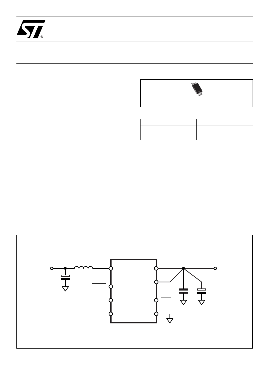
Figure 1. Application Circuit
L1
V
CC
2.5V 3.3V
February 2005
C2
LX
SHDN
LBI
REF
7
5
L6920D
2
4
OUT
8
V
OUT
FB
1
500mA
C3 C1
LBO
3
GND
6
Rev. 2
1/13
L6920
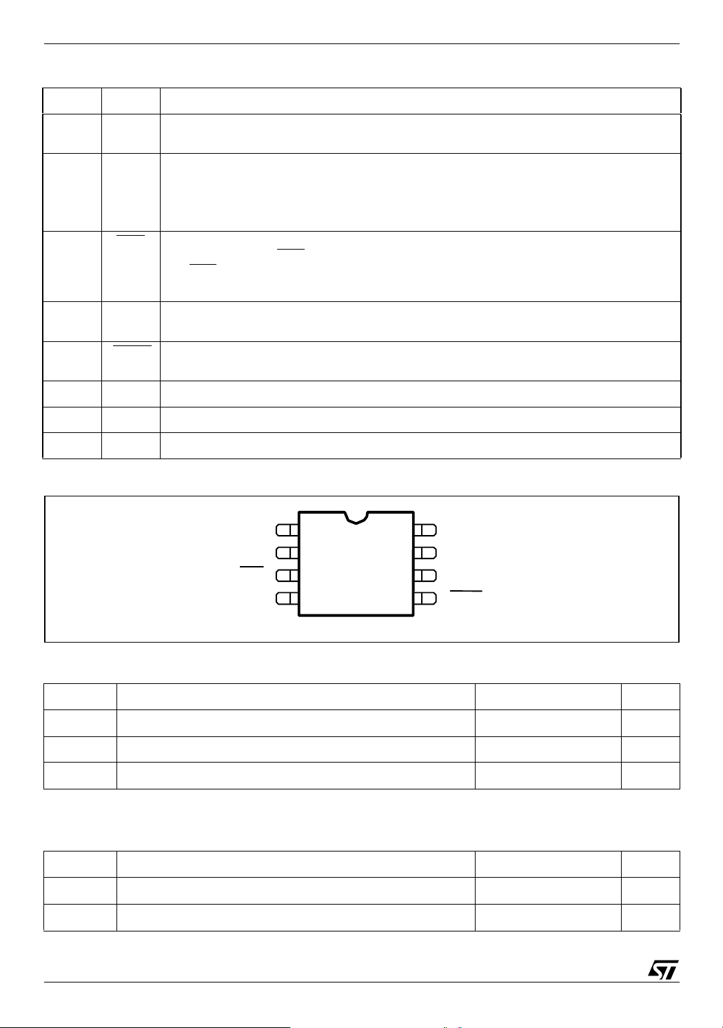
8
Table 1. Pin Description
Pin Name Function
1FB
Output voltage selector. Connect FB to GND for Vout=5V or to OUT for Vout=3.3V. Connect FB to an
external resistor divider for adjustable output voltage (from 2V to 5.2V) [see R4 and R5, fig. 7].
2 LBI Battery low voltage detector input. The internal threshold is set to 1.23V.
A resistor divider is needed to adjust the desired low battery threshold:
R1
V
LBI
3
LBO
Battery low voltage detector output. If the voltage at the LBI pin drops below the internal
⎛⎞
1.23V= 1
⋅
⎝⎠
[see R1 and R2, fig. 7]
------- -+
R2
threshold typ. 1.23V, LBO goes low.
LBO is an open drain output and so a pull-up resistor (about 200KΩ) has to be added for
The
correct output setting [see R3, fig. 7].
4 REF 1.23V reference voltage. Bypass this output to GND with a 100nF capacitor for filtering high
frequency noise. No capacitor is required for stability
5
SHDN
Shutdown pin. When pin 5 is below 0.2V the device is in shutdown, when pin 5 is above 0.6V the
device is operating.
6 GND Ground pin
7 LX Step-up inductor connection
8 OUT Power OUTPUT pin
Figure 2. Pin Connection (Top view)
FB
LBI
LBO
REF
8
2
3
4
TSSOP
7
6
5
OUT1
LX
GND
SHDN
Table 2. Absolute Maximum Ratings
Symbol Parameter Value Unit
V
ccmax
Vcc to GND 6 V
LBI, SHDN, FB to GND 6 V
V
out max
Vout to GND 6 V
Table 3. Thermal Data
Symbol Parameter Value Unit
R
th j-amb
T
Thermal Resistance Junction to Ambient 250 °C/W
Maximum Junction Temperature 150 °C
j
2/13
L6920
Table 4. Electrical Characteristcs
= 2V, FB = GND, T
(V
in
Symbol Parameter Test Condition Min. Typ. Max. Unit
SECTION
V
CC
V
Minimum operating Input Voltage 0.6 V
in
V
Minimum Start Up Input Voltage 1 V
in
= -40°C to 85°C and Tj < 125°C unless otherwise specified)
amb
Quiescent Current Il =0 mA, FB = 1.4V, V
I
q
I
Shut Down Current Vin = 5V, Il =0 mA 0.1 1 µA
sd
Irev Reverse battery current V
LBI = SHDN = 2V, T
Il =0 mA, FB = 1.4V, V
LBI = SHDN = 2V, T
= -4V, Tj = T
in
amb
= T
j
= T
j
= 3.3V
out
amb
= 5V
out
amb
915µA
11 18 µA
0.1 2 µA
POWER SECTION
on-N
on-P
Active switch ON resistance 120 250 mΩ
Synchronous switch ON
120 250 mΩ
R
R
resistance
CONTROL SECTION
V
t Output voltage FB = OUT, Il =0 mA 3.2 3.3 3.4 V
ou
FB = GND, I
=0 mA 4.955.1V
l
Output voltage range External divider 2 5.2 V
V
V
LBI threshold 1.18 1.23 1.27 V
LBI
< 70°C 1.205 1.23 1.255 V
j
< 250µA 0.20.4V
sink
LBO
LBO logic LOW
0°C < T
I
I
LX switch current limit 0.8 1 1.2 A
lim
T
onmax
T
offmin
Maximum on time V
Minimum off time V
SHDN SHDN logic LOW
SHDN logic HIGH
V
Reference Voltage 1.18 1.23 1.27 V
ref
= 2V to 5.3V 3.75 5 6.25 µs
out
= 2V to 5.3V 0.75 1 1.25 µs
out
0.2 V
0.6 V
3/13
L6920
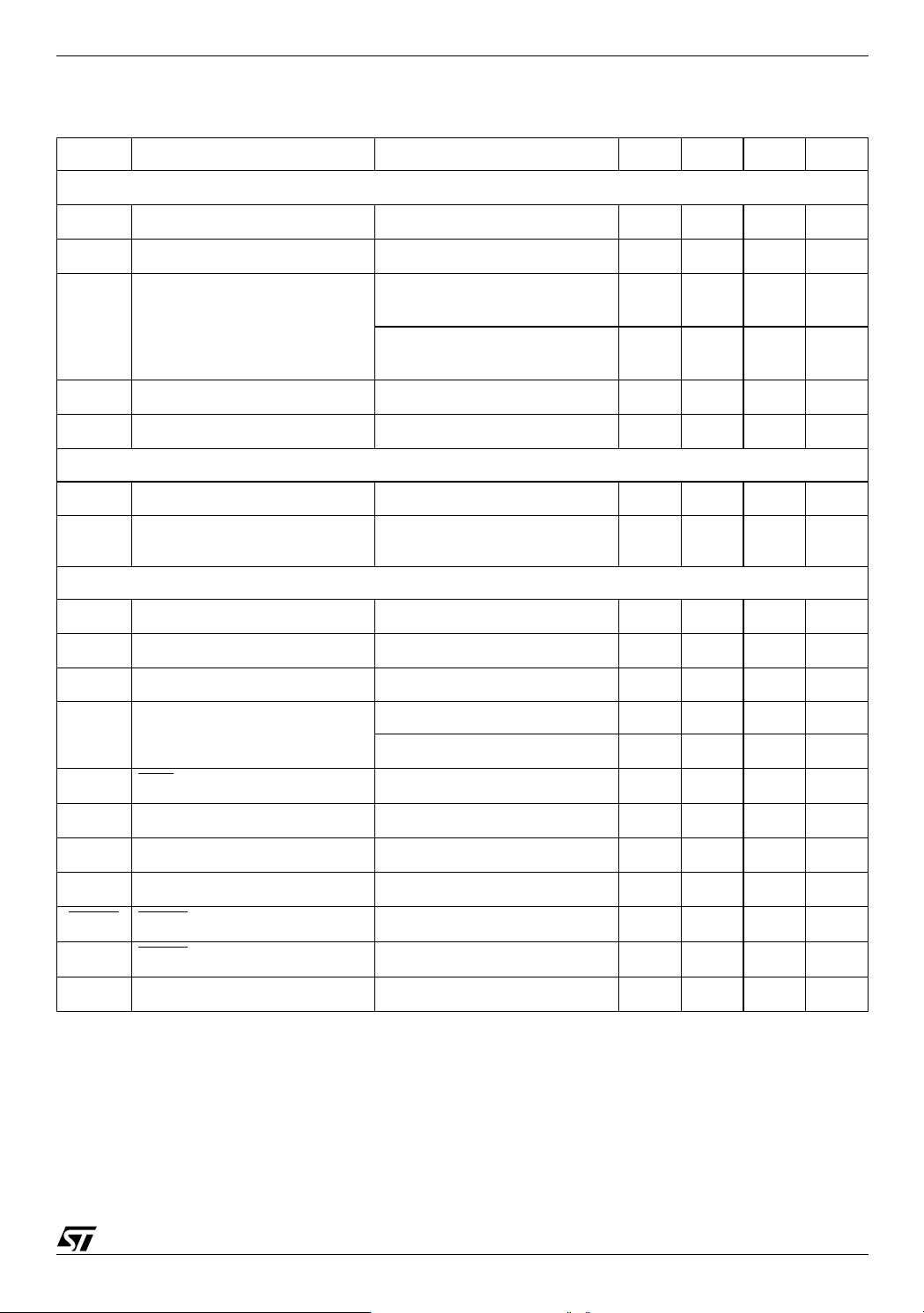
Figure 3.
Efficiency vs. Output Current
100
90
80
Vin = 1.2V
70
60
η [%]
50
EFFICIENCY
40
30
20
10
0
0.01 0.1 1 10 100 1000
Figure 4.
Efficiency vs. Output Current
100
90
80
LOAD CURRENT [ mA]
Vout = 3.3V
L = 47µH
C = 100µF
Vin = 1.2V
70
Vin = 2.4V
Vin = 3.6V
Vin = 2.4V
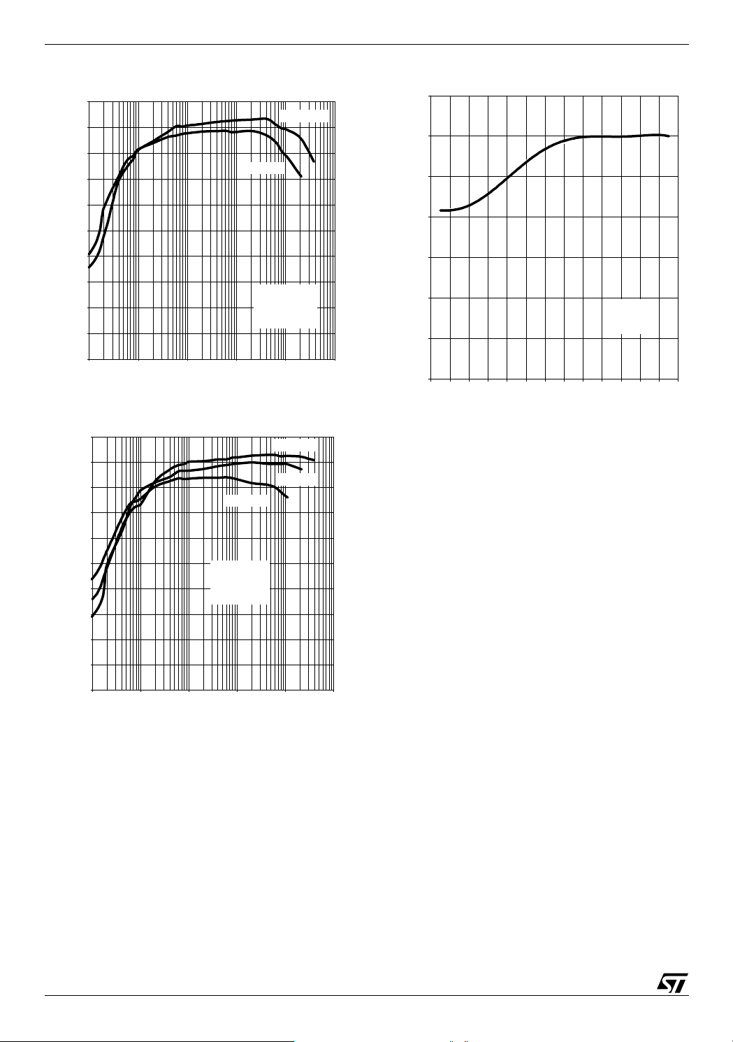
Figure 5. Startup Voltage vs Output Current
1.4
1.2
1
0.8
0.6
Startup voltage (V)
0.4
0.2
0
30 60 90 120 150 180
Output current (mA)
L = 47µH
C = 22µF
60
50
η [%]
EFFICIENCY
40
30
20
10
0
0.01 0.1 1 10 100 1000
f
Vout = 5V
L = 47µH
C = 100µF
LOAD CURRENT [mA]
4/13