

查询L6919E供应商
5 BIT PROGRAMMABLE DUAL-PHASE CONTROLLER
■ 2 PHASE OPERATION WITH
SYNCRHONOUS RECTIFIER CONTROL
■ ULTRA FAST LOAD TRANSIENT RESPONSE
■ INTEGRATED HIGH CURRENT GATE
DRIVERS: UP TO 2A GATE CURRENT
■ TTL-C O MPAT I BLE 5 BIT P R O GRAM MABL E
OUTPUT FROM 0.800V TO 1.550V WITH
25mV STEPS
■ DYNAMIC VID MANAGEMENT
■ 0.6% OUTPUT VOLTAGE ACCURACY
■
10% ACTIVE CURREN T SHARING ACCURACY
■ DIGITAL 2048 STEP SOFT-START
■ OVERVOLTAGE PROT ECTION
■ OVERCURRENT PROTECTION REALIZED
USING THE LOWER MOSFET'S R
SENSE RESISTOR
■ OSCILLATOR EXTERNALLY ADJUSTABLE
AND INTERNALLY FIXED AT 200kHz
■ POWER GOOD OUTPUT AND INHIBIT
FUNCTI ON
■ REMOTE SENSE BUFFER
■ PACKAGE: SO- 28
APPLICATIONS
■ POWER SUPPLY FOR SERVERS AND
WORKSTATIONS
■ POWER SUPPLY FOR HIGH CURRENT
MICROPROCESSORS
■ DISTRI BUTED POWER SUPPLY
dsON
L6919E
WITH DYNAMIC VID MANAGEMENT
SO-28
ORDERING NUMBERS:L6919E
L6919ETR
DESCRIPTION
The device is a power supply controller specifically
designed to provide a high performance DC/DC
conversion for high current microprocessors. The
device implements a dual-phase s tep-down con-
OR A
troller with a 180° phase-shift between each
phase. A precise 5-bit digital to analog con verter
(DAC) allows adjusting the output voltage from
0.800V to 1.550V with 25mV binary steps managing On-The-Fly VID code changes.
The high precision internal reference assures the
selected output voltage to be within ± 0.6%. The
high peak current gate drive affords to have fast
switching to the external power mos providing low
switching losses .
The device assures a fast protecti on against load
over current and load over/under voltage. An internal crowbar is provided turning on the low side
mosfet if an over-voltage is detected. In case of
over-current, the system works in Constant Current mode.
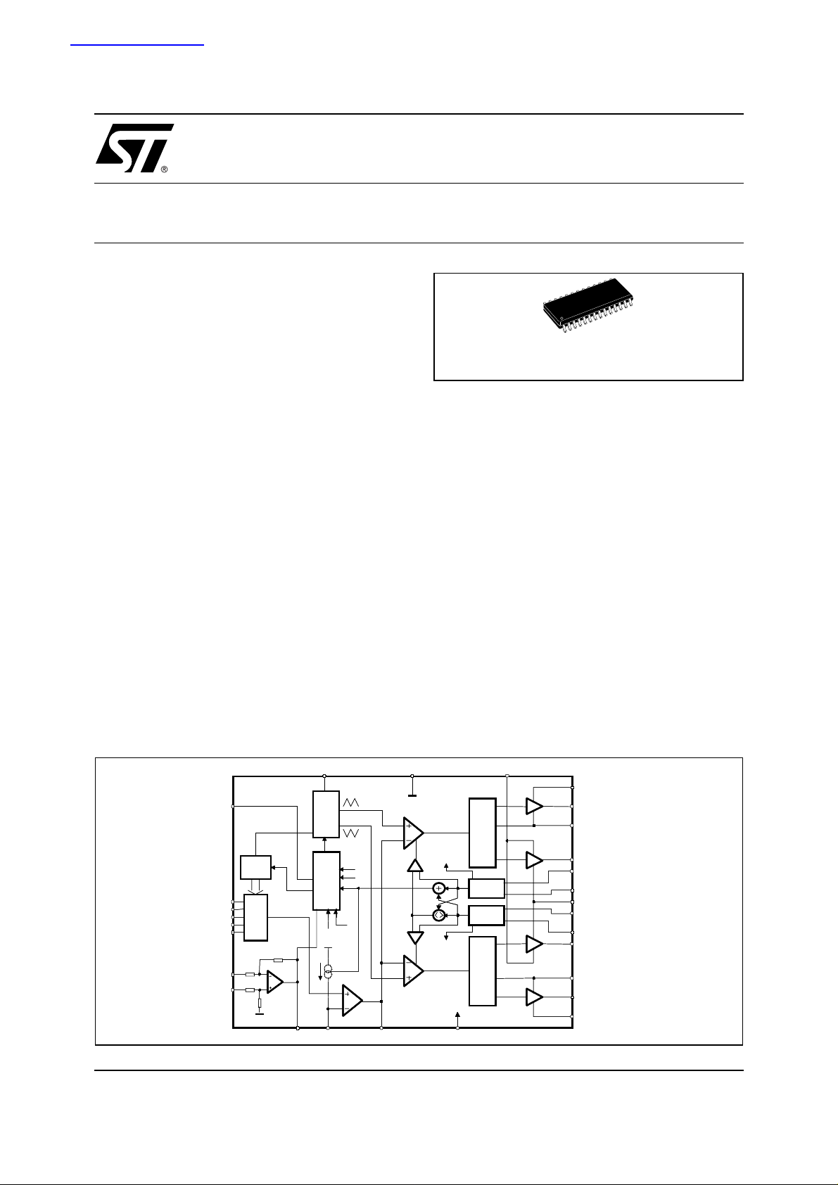
BLOCK DIAGRAM
PGOOD
PGOOD
September 2003
VID4
VID4
VID3
VID3
VID2
VID2
VID1
VID1
VID0
VID0
FBG
FBG
FBR
FBR
DIGITAL
DIGITAL
SOFT-STAR T
SOFT-STAR T
DAC
DAC
32k
32k
32k
32k
32k
32k
32k
32k
REMOTE
REMOTE
BUFFER
BUFFER
OSC /INH SGND VCCDR
OSC /INH SGND VCCDR
PWM1
TO TA L
TO TA L
CURRENT
CURRENT
CURRENT
CURRENT
PWM1
PWM2
PWM2
LOGIC PWM
LOGIC PWM
LOGIC PWM
ADAPTIVE ANTI
ADAPTIVE ANTI
CH1
CH1
OCP
OCP
CURRENT
CURRENT
CORR ECTION
CORR ECTION
AVG
AVG
CH2
CH2
OCP
OCP
CURRENT
CURRENT
CORRECTION
CORRECTION
ADAPTIVE ANTI
CRO SS COND UCT ION
CRO SS COND UCT ION
CRO SS COND UCT ION
CURRENT
CURRENT
CURRENT
READING
READING
READING
CURRENT
CURRENT
CURRENT
READING
READING
READING
LOGIC PW M
LOGIC PW M
LOGIC PW M
ADAPTIVE ANTI
ADAPTIVE ANTI
ADAPTIVE ANTI
CROSS CONDUCTION
CROSS CONDUCTION
CROSS CONDUCTION
Vcc
Vcc
VccCOM PFBVSEN
VccCOM PFBVSEN
I
I
FB
FB
2 PHASE
2 PHASE
LOGIC AND
LOGIC AND
CH1 OCP
CH1 OCP
OSCI LLATO R
OSCI LLATO R
PROTECTIONS
PROTECTIONS
CH2 OCP
CH2 OCP
VCC
VCC
VCCDR
VCCDR
ERR OR
ERR OR
AMPLIFIER
AMPLIFIER
BOO T1
BOO T1
HS
HS
LS
LS
LS
LS
HS
HS
U
U
GAT E1
GAT E1
PHASE1
PHASE1
LGATE1
LGATE1
ISEN1
ISEN1
PGNDS1
PGNDS1
PGND
PGND
PGNDS2
PGNDS2
ISEN2
ISEN2
LGATE2
LGATE2
PHASE2
PHASE2
UGATE2
UGATE2
BOO T2
BOO T2
1/33
L6919E
R
ABSOLUTE MAXIMUM RATINGS
Symbol Parameter Value Unit
Vcc, V
CCDR
V
BOOT-VPHASE
V
UGATE1-VPHASE1
V
UGATE2-VPHASE2
V
phase
UGATEx Pin Maximum Withstanding Voltage Range
OTHER PINS ±2000 V
THERMAL DATA
Symbol Parameter Value Unit
to PGND 15 V
Boot Voltage 15 V
15 V
LGATE1, PHASE1, LGATE2, PHASE2 to PGND -0.3 to Vcc+0.3 V
VID0 to VID4 -0.3 to 5 V
All other pins to PGND -0.3 to 7 V
Sustainable Peak Voltage t < 20ns @ 600kHz 26 V
±1000 V
Test Conditio n: CDF-AEC-Q100-002”Human Body Model
Acceptance Criteria: “Normal Performance”
”
R
th j-amb
T
T
storage
P
PIN CONNECTION
Thermal Resistance Junction to Ambient 60 °C/W
Maximum junction temperatu re 150 °C
max
Storage temperature range -40 to 150 °C
T
Junction Temperature Range 0 to 125 °C
j
Max power dissipation at T
MAX
= 25°C 2 W
amb
LGATE1
1
VCCDR
PHASE1
UGATE1
BOOT1
VCC
SGND
COMP
FB
VSEN
FB
FBG
ISEN1
PGNDS1
2
3
4
5
6
7
8
9
10
11
12
13
14
28
27
26
25
24
L6919E
23
22
21
20
19
18
17
16
15
PGND
LGATE2
PHASE2
UGATE2
BOOT2
PGOOD
VID4
VID3
VID2
VID1
VID0
OSC / INH / FAULT
ISEN2
PGNDS
2/33

L6919E
ELECTRICAL CHARACTERISTICS
V
= 12V
CC
Symbol Parameter Test Condition Min Typ Max Unit
Vcc SUPPLY CURRENT
±15%
, TJ = 0 to 70°C unless otherwise specified
I
I
CCDR
I
BOOTx
Vcc supply current HGATEx and LGATEx open
CC
V
supply current LGATEx open; V
CCDR
Boot supply current HGATEx open; PHASEx to PGND
POWER-ON
Turn-On V
Turn-Off V
Turn-On V
threshold VCC Rising; V
CC
threshold VCC Falling; V
CC
CCDR
Threshold
Turn-Off V
CCDR
Threshold
OSCILLATOR/INHIBIT/FAULT
f
OSC
Initial Accuracy OSC = OPEN
INH Inhibit threshold I
d
MAX
Maximum duty cycle OSC = OPEN; IFB = 0 72 80 %
7.5 10 12.5 mA
V
CCDR=VBOOT
=12V
=12V 2 3 4 mA
CCDR
0.5 1 1.5 mA
V
CC=VBOOT
V
CCDR
V
=12V
CC
V
CCDR
=12V
Rising
Falling
=5V 8.2 9.2 10.2 V
CCDR
=5V 6.5 7.5 8.5 V
CCDR
4.2 4.4 4.6 V
4.0 4.2 4.4 V
VCC=12V
OSC = OPEN; Tj=0°C to 125°C
=5mA 0.5 V
SINK
OSC = OPEN; I
= 70µA3040 %
FB
127
135
150 165
178
kHz
kHz
∆Vosc Ramp Amplitude 3 V
FAULT Voltage at pin OSC OVP or UVP Active 4.75 5.0 5.25 V
REFERENCE AND DAC
I
DAC
Output Voltage
Accuracy
VID pull-up Current VIDx = GND 4 5 6 µA
VID0, VID1, VID2, VID3, VID4
see Table1;
FBR = V
; FBG = GND
OUT
-0.6 - 0.6 %
VID pull-up Voltage VIDx = OPEN 2.9 - 3.3 V
ERROR AMPLIFIER
DC Gain 80 dB
SR Slew-Rate COMP=10pF 15 V/µs
DIFFERENTIAL AMPLIFIER (REMOTE BUFFER)
DC Gain 1 V/V
CMRR Common Mode Rejection Ratio 40 dB
SR Slew Rate VSEN=10pF 15 V/µs
3/33

L6919E
ELECTRICAL CHARACTERISTICS (continued)
V
= 12V
CC
Symbol Parameter Test Condition Min Typ Max Unit
DIFFERENTIAL CURRENT SENSING
I
ISEN1
I
ISEN2
±15%
, TJ = 0 to 70°C unless otherwise specified
,
Bias Current I
= 0 45 50 55 µA
LOAD
I
PGNDSx
I
ISEN1
I
ISEN2
I
Bias Current 45 50 55 µA
,
Bias Current at
Over Current Threshold
Active Droop Current I
FB
GATE DRIVERS
t
RISE
HGATE
I
HGATEx
High Side
Rise Time
High Side
Source Current
R
HGATEx
High Side
Sink Resistance
t
RISE
LGATE
I
LGATEx
Low Side
Rise Time
Low Side
Source Current
R
LGATEx
Low Side
Sink Resistance
PROTECTIONS
PGOOD Upper Threshold
(V
/DAC Output)
SEN
80 85 9 0 µA
≤ 0%
LOAD
I
= 100%
LOAD
V
BOOTx-VPHASEx
C
V
V
V
C
V
V
V
to PHASEx=3.3nF
HGATEx
BOOTx-VPHASEx
BOOTx-VPHASEx
=10V;
CCDR
to PGNDx=5.6nF
LGATEx
=10V 1.8 A
CCDR
=12V 0.7 1.1 1.5 Ω
CCDR
Rising 108 112 116 %
SEN
=10V;
=10V 2 A
=12V; 1.5 2 2.5 Ω
47.5
0
50
15 30 ns
30 55 ns
1
52.5
µA
µA
PGOOD Lower Threshold
(V
/DAC Output)
SEN
OVP Over Voltage Threshold
(V
)
SEN
UVP Under Voltage Trip
(V
/DAC Output)
SEN
V
PGOODL
I
PGOODH
PGOOD Voltage Low I
PGOOD Leakage V
4/33
V
Falling 84 88 92 %
SEN
V
Rising 1.915 2.05 V
SEN
V
Falling 55 60 65 %
SEN
= -4mA 0.4 V
PGOOD
= 5V 1 µA
PGOOD
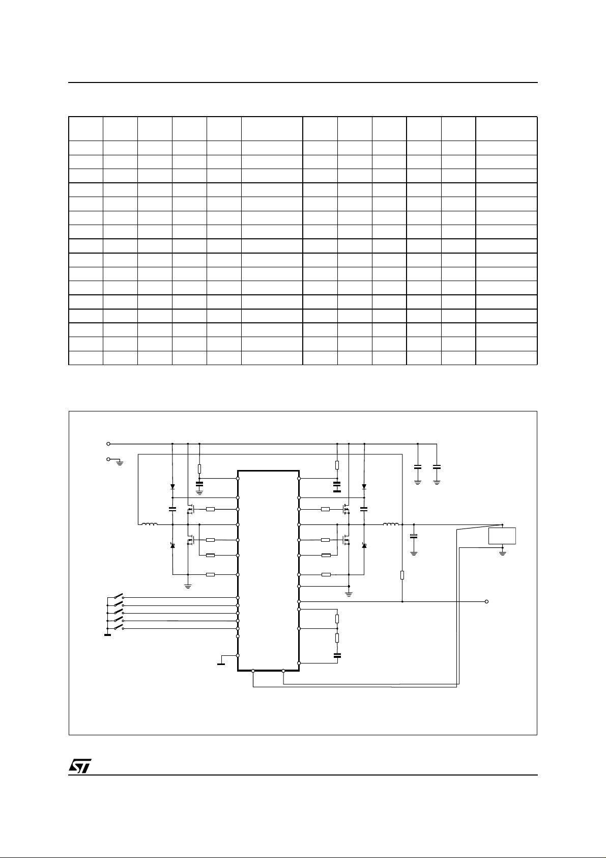
Table 1. Voltage Identification (VID) Codes
VID4 VID3 VID2 VID1 VID0
00000 1.575 10000 1.175
00001 1.550 10001 1.150
00010 1.525 10010 1.125
00011 1.500 10011 1.100
00100 1.475 10100 1.075
00101 1.450 10101 1.050
00110 1.425 10110 1.025
00111 1.400 10111 1.000
01000 1.375 11000 0.975
01001 1.350 11001 0.950
01010 1.325 11010 0.925
01011 1.300 11011 0.900
01100 1.275 11100 0.875
01101 1.250 11101 0.850
01110 1.225 11110 0.825
01111 1.200 11111Shutdown
The device automatically regulates 25m V higher than the Hammer specs avoid ing the use of any external offset resistor
Output
Voltage (V)
VID4 VID3 VID2 VID1 VID0
Voltage (V)
L6919E
Output
Reference Schematic
Vin
GNDin
L1
S4
S3
S2
S1
S0
HS1
LS1
C
IN
24
25
26
27
16
15
28
23
10
VCC
6
BOOT2
UGATE2
PHASE2
LGATE2
ISEN2
Rg
PGNDS2
PGND
Rg
PGOOD
VSEN
FB
9
COMP
8
HS2
L2
LS2
C
OUT
LOAD
PGOOD
R
FB
R
F
C
F
VCCDR
2
BOOT1
5
UGATE1
PHASE1
LGATE1
ISEN1
PGNDS1
VID4
VID3
VID2
VID1
VID0
OSC / INH
SGND
4
3
1
13
14
L6919E
22
21
20
19
18
17
7
11 12
FBR FBG
Rg
Rg
5/33

L6919E
PIN FUNCTION
N Nam e Description
1 LGATE1 Channel 1 LS driver output.
A little series resistor helps in reducing device-dissipated power.
2 VCCDR LS drivers supply: it can be varied from 5V to 12V buses.
Filter locally with at least 1µF ceramic cap vs. PGND.
3 PHASE1 Channel 1 HS driver return path. It must be connected to the HS1 mosfet source and provides
4 UGATE1 Channel 1 HS driver output.
5 BOOT1 Channel 1 HS driver supply. This pin supplies the relative high side driver.
6 VCC Device supply voltage. The operative supply voltage is 12V ±10%.
7 GND All the internal references are referred to this pin. Connect it to the PCB signal ground.
8 COMP This pin is connected to the error amplifier output and is used to compensate the control
9 FB This pin is connected to the error amplifier inverting input and is used to compensate the
10 VSEN Manages Over&Under-voltage conditions and the PGOOD signal. It is internally connected with
11 FBR Remote sense buffer non-inverting input. It has to be connected to the positive side of the load
12 FBG Remote sense buffer inverting input. It has to be connected to the negative side of the load to
13 ISEN1 Channel 1 current sense pin. The output current may be sensed across a sense resistor or
14 PGNDS1 Channel 1 Power Ground sense pin. The net connecting the pin to the sense point must be
15 PGNDS2 Channel 2 Power Ground sense pin. The net connecting the pin to the sense point must be
16 ISEN2 Channel 2 current sense pin. The output current may be sensed across a sense resistor or
the return path for the HS driver of channel 1.
A little series resistor helps in reducing device-dissipated power.
Connect through a capacitor (100nF typ.) to the PHASE1 pin and through a diode to VCC
(cathode vs. boot).
Filter with 1µF (Typ.) capacitor vs. GND.
feedback loop.
voltage control feedback loop.
A current proportional to the sum of the current sensed in both channel is sourced from this pin
(50µA at full load, 70µA at the Constant Current threshold). Connecting a resistor between this
pin and VSEN pin allows programming the droop effect.
the output of the Remote Sense Buffer for Remote Sense of the regulated voltage.
If no Remote Sense is implemented, connect it directly to the regulated voltage in order to
manage OVP, UVP and PGOOD.
Connecting 1nF capacitor max vs. SGND can help in reducing noise injection.
to perform a remote sense.
If no remote sense is implemented, connect directly to the output voltage (in this case connect
also the VSEN pin directly to the output regulated voltage).
perform a remote sense.
Pull-down to ground if no remote sense is implemented.
across the low-side mosfet R
to the sense resistor through a resistor Rg.
The net connecting the pin to the sense point must be routed as close as possible to the
PGNDS net in order to couple in common mode any picked-up noise.
routed as close as possible to the ISEN1 net in order to couple in common mode any picked-up
noise.
routed as close as possible to the ISEN2 net in order to couple in common mode any picked-up
noise.
across the low-side mosfet R
to the sense resistor through a resistor Rg.
The net connecting the pin to the sense point must be routed as close as possible to the
PGNDS net in order to couple in common mode any picked-up noise.
This pin has to be connected to the low-side mosfet drain or
dsON.
This pin has to be connected to the low-side mosfet drain or
dsON.
6/33

L6919E
PIN FUNCTION
N Name Description
17 OSC/INH
18-22 VID4-0 Voltage IDentification pins.
23 PGOOD This pin is an open collector output and is pulled low if the output voltage is not within the above
24 BOOT2 Channel 2 HS driver supply. This pin supplies the relative high side driver.
25 UGATE2 Channel 2 HS driver output.
26 PHASE2 Channel 2 HS driver return path. It must be connected to the HS2 mosfet source and provides
27 LGATE2 Channel 2 LS driver output.
28 PGND LS drivers return path.
(continued)
FAULT
Oscillator pin.
It allows programming the switching frequency of each channel: the equivalent switching
frequency at the load side results in being doubled.
Internally fixed at 1.24V, the frequency is varied proportionally to the current sunk (forced) from
(into) the pin with an internal gain of 6kHz/µA (See relevant section for details). If the pin is not
connected, the switching frequency is 150kHz for each channel (300kHz on the load).
The pin is forced high (5V Typ.) when an Over/Under Voltage is detected; to recover from this
condition, cycle VCC.
Forcing the pin to a voltage lower than 0.6V, the device stop operation and enter the inhibit
state.
Internally pulled-up, connect to GND to program a ‘0’ while leave floating to program a ‘1’.
They are used to program the output voltage as specified in Table 1 and to set the PGOOD,
OVP and UVP thresholds.
The device automatically regulates 25mV higher than the HAMMER DAC avoiding the use of
any external set-up resistor.
specified thresholds and during soft start. It cannot be pulled-up above 5V.
If not used may be left floating.
Connect through a capacitor (100nF typ.) to the PHASE2 pin and through a diode to VCC
(cathode vs. boot).
A little series resistor helps in reducing device-dissipated power.
the return path for the HS driver of channel 2.
A little series resistor helps in reducing device-dissipated power.
This pin is common to both sections and it must be connected through the closest path to the
LS mosfets source pins in order to reduce the noise injection into the device.
7/33
L6919E
DEVICE DESCRIPTION
The device is an integrated circuit realized in BCD technology. It provides complete control logic and protections for
a high performance dual-phase step-down DC-DC converter optimized for microprocessor power supply. It is designed to drive N Channel MOSFETs in a dual-phase synchronous-rectified buck topology. A 180 deg phase shift is
provided between the two phases allowing reduction in the input capacitor current ripple, reducing also the size and
the losses. The output vo ltage of the co nverte r can be precise ly regul ated, prog rammi ng the VID pins, from 0.825V to
1.575V with 25mV bina ry steps, with a maxim um tolerance of ±0.6 % over temperature and l ine voltage variat ions. The
device aut om ati cally regulates 25mV higher than the HAMMER DAC avoiding the use of any external set-up resistor.
The device manages On-Th e-Fly VID Code chang es stepp ing to the ne w confi guration f ollow ing the VID tabl e with no
need for external components. The device provides an average current-mode control with fast transient response. It
includes a 150kHz free-running oscillator. The error am pl if i er f eatures a 15V/
bandwidth for fast transient performances. Current information is read across the lower mosfets RdsON or across a
sense resist or i n fully differential mode. The current information corrects the PWM output i n order to equ alize the average cu rr ent carried by each phase. Current sharing between the two phases i s then limited at ±10% over static a nd
dynamic c ondi tions. The device protect s against Over- C urr ent , with an OC thr eshold for each phase, en tering in constant current mode. Since the current is read across the low side mosfets, the constant current keeps constant the
bottom of the inductors current triangular waveform. When an under voltage is detected the device latches and the
FAULT pin is dri ven high. The devi ce performs also Over-Volta ge protection t hat disables i mmediately the device turning ON the lower driver and driving high the FAULT pin.
OSCILLATOR
The switching frequency is internally fixed at 150kHz. Each phase works at the frequency fixed by the oscillator so
that the result ing switching frequency at the load side results in being doubled.
The internal oscillator generates the triangular waveform for the PWM charging and discharging with a constant current an in ter nal c apac itor . The curre nt deliv ere d to th e os cilla tor is typ icall y 25 A (F sw=150kHz) and may be varied
using an external resist or (ROSC) connected between OSC pin and GND or Vcc. Since the OSC pin is m ai ntained at
fixed voltage (Typ. 1.237V), th e fr equency is varied proportionally to the current sunk (f or ced) from (into) the pin considering the internal gain of 6KHz/
µ
A.
In particular connecting it to GND the frequency is increased (current is sunk from the pin), while connecting ROSC
to Vcc=12V the freq uency is reduced (current is for ced i nto the pin), according to the fo llowing relationships :
vs. GND: fS150kHz
R
OSC
1.237
---------------
R
OSC
kHz
-----------
6
⋅+ 150kHz
µA
µ
s slew rate that per mits high converter
6
⋅
7.422 10
----------------------------- -+==
R
OSC
KΩ()
7
⋅
KΩ()
R
OSC
vs. 12V: f
S
150kHz
12 1.237–
---------------------------
R
OSC
kHz
-----------
6
⋅– 150kHz
µA
6.457 10
------------------------------–==
R
OSC
Note that forcing a 25µA into this pin, the device stops switching because no current is delivered to the oscillator.
Figure 1. R
8/33
vs. Switching Frequency
OSC
14000
12000
10000
8000
) vs. 12V
Ω
Ω
Ω
Ω
6000
4000
Rosc(K
2000
0
25 50 75 100 125 150
Frequency (KHz)
800
700
600
500
) vs. GND
400
Ω
Ω
Ω
Ω
300
200
Rosc(K
100
0
150 250 350 450 550 650
Frequency (KHz)

L6919E
DIGITAL TO ANALOG CONVERTER
The built-in digital to analog converter allows the adjustment of the output voltage from 0.800V to 1.550V with
25mV as shown in the previous table 1. The internal reference is trimmed to ensure output voltage precision of
±0.6% and a zero temperature coefficient around 70°C. The internal reference voltage for the reg ulation is programmed by the voltage identification (VID) pins. These are TTL compatible inputs of an internal DAC that is
realized by means of a series of resistors providing a partition of the internal voltage reference. The VID code
drives a multiplexer that selects a voltage on a precise point of the divider. The DAC output is delivered to an
amplifier obtaining the V
provided (realized with a 5
to leave the pin floating, while to program a logic "0" it is enough to short the pin to GND. Programming the
"11111" code, the device enters the NOCPU mode: all mosfets are turned OFF and protections are disabled.
The condition is latched.
The voltage identification (VID) pin configuration also sets the power-good thresholds (PGOOD) and the Over
/ Under Voltage protection (OVP/UVP) thresholds.
DYNAMIC VID TRANSITION
The device is able to manage On-The-Fly VID Code changes that allow Output Voltage modification during normal device operation. The device checks every clock cycle (synchronously with the PWM ramp) for VID code
modifications. Once the new code is stable for more than one clock cycle, the reference steps up or down in
25mV increments every c lock cycle until the new VID code is reached. D uring the transiti on, VID code c hanges
are ignored; the devi ce re- starts monit oring V ID after the transiti on has finis hed. P GOOD, signal is mask ed during the transition and it is re-activated after the transition has finished while OVP / UVP are still active.
voltage reference (i.e. the set-point of the error amplifier). Internal pull-ups are
PROG
µ
A current generator up to 3.0V Typ); in this way, to program a logic "1" it is enough
Figure 2. Dynamic VID transition
VID
Reference
25mV steps transition
V
OUT
1 Clock Cycle Blanking Time
DRIVER SECTION
The integrated high-current drivers allow using different types of power MOS (also multiple MOS to reduce the
R
), maintaining fast switching transition.
dsON
The drivers for the high-side mosfets use BOOTx pins for supply and PHASEx pins for return. The drivers for
the low-side mosfets use VCCDRV pin for supply and PGND pin for return. A minimum voltage of 4.6V at VCCDRV pin is required to start operations of the device.
The controller embodies a sophisticated anti-shoot-through system to minimize low side body diode conduction
time maintaining good efficiency saving the use of Schottky diodes. The dead time is reduced to few nanoseconds assuring that high-side and low-side mosfets are never switched on simultaneously: when the high-side
mosfet turns off, the voltage on its source begins to fall; when the voltage reach es 2V, the low-side mosfet gate
drive is applied with 30ns delay. When the low-side mo sfet turns off, the v oltage at LGATEx pin i s sensed. When
it drops below 1V, the high-side mosfet gate drive is applied with a delay of 30ns. If the current flowing in the
inductor is negative, the source of high-side mosfet will never drop.
t
t
t
9/33
L6919E
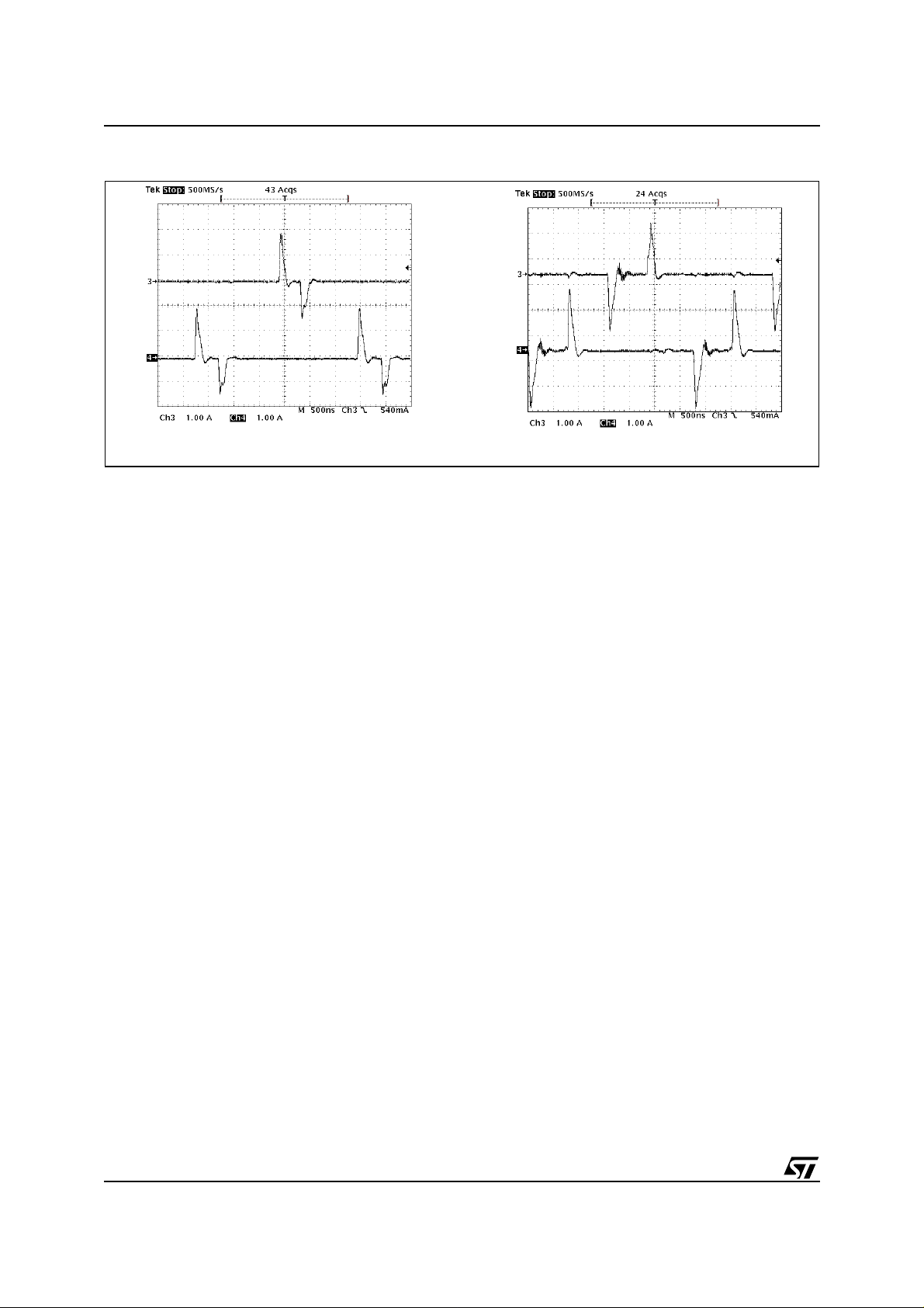
Figure 3. Drivers peak current: High Side (left) and Low Side (right)
CH3 = HGATE1; CH4 = HGATE2 CH3 = LGATE1; CH4 = LGATE2
To allow the turning on of the low-side mosfet even in this case, a watchdog controller is enabled: if the source
of the high-side mosfet don't drop for more than 240ns, the low side mosfet is switched on so allowing the negative current of the inductor to recirculate. This mechanism allows the system to regulate even if the current is
negative.
The BOOTx and VCCDR pins are separated from IC's power supply (VCC pin) as well as signal ground (SGND
pin) and power ground (PGND pin) in order to maximize the switching noise immunity. The separated supply
for the diff erent drivers gives high flexibility in mosfet choice, allow ing the use of logic-lev el mosfet. S everal combination of supply can be chosen to optimize performance and efficiency of the application. Power conversion
is also flexible; 5V or 12V bus can be chosen freely.
The peak current is shown for both the upper and the lower driver of the two phases in figure 3. A 10nF capacitive load has been used. For the upper drivers, the source current is 1.9A while the sink current is 1.5A with
V
BOOT -VPHASE
VCCDR = 1 2V.
= 12V; similar ly, for the lower driv ers, the sour ce c urrent is 2.4A while the sink cur rent is 2A w ith
CURRENT READING AND OVER CURRENT
The current flowing trough each phase is read using the voltage drop across the low side mosfets R
across a sense resistor (R
) and internally converted into a current. The Tran conductance ratio is issued
SENSE
dsON
or
by the external resistor R g placed outsi de the chip between ISEN x and PGNDSx pins toward the reading points.
The full differential current readi ng rejects noi se and allow s to place sensing el ement in differ ent lo cations without affecting the measurement's accuracy. The current reading circuitry reads the current during the time in
which the low-side mosfet is on (OFF Time). During this time, the reaction keeps the pin ISENx and PGNDSx
at the same voltage while during the time in w hich th e reading circ uitry is off, an internal clamp ke eps these two
pins at the same voltage sinking from the ISENx pin the necessary current (Needed if low-side mosfet R
dsON
sense is implemented to avoid absolute maximum rating overcome on ISENx pin).
The proprietary current reading circuit allows a very precise and high bandwidth reading for both positive and
negative current. This circuit reproduces the current flowing through the sensing element using a high speed
Track & Hold Tran conductance amplifier. In particular, it reads the current during the second half of the OFF
time reducing noise injection into the device due to the mosfet turn-on (See fig. 4). Track time must be at least
200ns to make proper reading of the delivered current
This circuit sources a constant 50
µ
A current from the PGNDSx pin and keeps the pins ISENx and PGNDSx at
the same voltage. Referring to figure 4, the current that flows in the ISENx pin is then given by the following
equation:
10/33
I
ISENx
50µA
R
SENSEIPHASE
----------------------------------------------+ 50µAI
R
⋅
g
+==
INFOx
 Loading...