


查询L6917供应商
5 BIT PROGRAMMABLE DUAL-PHASE CONTROLLER
■
2 PHASE OPERATION WITH
SYNCRHONOUS RECTIFIER CONTROL
■
ULTRA FAST LOAD TRANSIENT RESPONSE
■
INTEGRATED HIGH CURRENT GATE
DRIVERS: UP TO 2A GATE CURRENT
■
TTL-COMP A T I BLE 5 BIT P ROGR AMMABLE
OUTPUT CO MPLIANT WITH VRM 9.0
■
0.8% INTERNAL REFERENCE ACCURACY
■
10% ACTIVE CURRENT SHARING
ACCURACY
■
DIGITAL 2048 STEP SOFT-START
■
OVERVOLTAGE PROTEC T I O N
■
OVERCURRENT PROTECTION REALIZED
USING THE LOWER MOSFET'S R
SENSE RESISTOR
■
300 kHz INTERNAL OSCILLATOR
■
OSCILLATOR EXTERNALLY ADJUST ABLE
UP TO 600kHz
■
POWER GOOD OUTPUT AND INHIBIT
FUNCTI ON
■
REMOTE SENSE BUFFER
■
PACKAGE: SO-28
APPLICATION S
■
POWER SUPPLY FOR SERVERS AND
WORKSTATIONS
■
POWER SUPPLY FOR HIGH CURRENT
MICROPROCESSORS
■
DISTRIBUTED DC-DC CONVERTERS
dsON
OR A
L6917B
SO-28
ORDERING NUMB ERS :L691 7BD
L6917BDTR (Tape & Reel)
DESCRIPTION
The device is a power supply controller specifically
designed to provide a high performance DC/DC conversion for high current microprocessors.
The device implements a dual-phase step-dow n controller with a 180° phase-shift between each phase.
A precise 5-bit digital to analog converter (DAC) allows adjusting the output voltage from 1.100V to
1.850V with 25mV binary steps.
The high precision internal r eference ass ures the selected output voltage to be within ±0.8%. The high
peak current gate drive affor ds to hav e fast s witching
to the external power mos providing low switching
losses.
The device assures a fast protection against load
over current and load over/under vol t age. An internal
crowbar is provided turning on the low side mosfet if
an over-voltage is detected. In case of over-current,
the system works in Constant Current mode.
BLOCK DIAGRAM
September 2002
PGOOD
VID4
VID3
VID2
VID1
VID0
FBG
FBR
DIGITAL
SOFT START
DAC
10k
10k
10k
10k
REMOTE
BUFFER
VSEN
ROSC / IN H
2 PHASE
OSCILLATOR
LOGIC
AND
PROTECTIONS
CH1 OVER
CURRENT
IFB
FB
CH2 OVER
CURRENT
VCC
VCCDR
ERROR
AMPLIFIER
SGND VCCDR
PWM1
-
+
CH 1 OVER
CURRENT
CURRENT
CORRECT ION
TOTAL
+
CURRENT
AVG
CURRENT
< >
CH 2 OVER
CURRENT
CURRENT
CORRECT ION
+
-
PWM2
LOGIC PWM
ADAPTIVE ANTI
CROSS-CONDUCTION
CURRENT
READING
CURRENT
READING
LOGIC PWM
ADAPTIVE ANTI
CROSS-CONDUCTION
Vcc
VccCOMP
BOOT1
HS
LS
LS
HS
UGATE1
PHASE1
LGATE 1
ISEN1
PGNDS1
PGND
PGNDS2
ISEN2
LGATE 2
PHASE2
UGATE2
BOOT2
1/33

L6917B
T
ABSOLUTE MAXIMUM RATINGS
Symbol Parameter Value Unit
Vcc, V
CCDR
V
BOOT-VPHASE
V
UGATE1-VPHASE1
V
UGATE2-VPHASE2
to PGND 15 V
Boot Voltage 15 V
15 V
LGATE1, PHASE1, LGATE2, PHASE2 to PGND -0.3 to Vcc+0.3 V
All other pins to PGND -0.3 to 7 V
V
phase
Sustainable Peak Voltage t < 20ns @ 600kHz 26 V
THERMAL DATA
Symbol Parameter Value Unit
R
th j-amb
T
T
storage
P
Thermal Resistance Junction to Ambient 60 °C/W
Maximum junction temperature 150 °C
max
Storage temperature range -40 to 150 °C
T
Junction Temperature Range -25 to 125 °C
j
Max power dissipation at T
MAX
= 25°C 2 W
amb
PIN CONNECTION
LGATE1
VCCDR
PHASE1
UGATE1
BOOT1
VCC
GND
COMP
FB
FBR
FBG
ISEN1
PGNDS1
2
3
4
5
6
7
8
9
10VSEN
11
12
13
14
SO28
28
27
26
25
24
23
22
21
20
19
18
17
16
15
PGND1
LGA TE2
PHASE2
UGATE2
BOOT2
PGOOD
VID4
VID3
VID2
VID1
VID0
OSC / INH / FAUL
ISEN2
PGNDS2
2/33

L6917B
ELECTRICAL CHARACTERISTICS
= 12V ±10%, TJ = 0 to 70°C unless otherwise specified
V
CC
Symbol Parameter Test Condition Min Typ Max Unit
Vcc SUPPLY CURRENT
I
I
CCDR
I
BOOTx
Vcc supply current HGATEx and LGATEx open
CC
V
supply current LGATEx open; V
CCDR
Boot supply current HGATEx open; PHASEx to PGND
POWER-ON
Turn-On V
threshold VCC Rising; V
CC
Turn-Off VCC threshold VCC Falling; V
Turn-On V
CCDR
Threshold
Turn-Off V
CCDR
Threshold
OSCILLATOR/INHIBIT/FAULT
f
OSC
f
OSC,Rosc
Initial Accuracy OSC = OPEN
Total Accuracy RT to GND=74kΩ 450 500 550 kHz
INH Inhibit threshold I
d
Maximum duty cycle OSC = OPEN 70 75 %
MAX
V
CCDR=VBOOT
=12V
=12V 2 3 4 mA
CCDR
0.5 1 1.5 mA
7.5 10 12.5 mA
V
CC=VBOOT
V
CCDR
=12V
Rising
=5V 7.8 9 10.2 V
CCDR
=5V 6.5 7.5 8.5 V
CCDR
4.2 4.4 4.6 V
VCC=12V
V
CCDR
Falling
4.0 4.2 4.4 V
VCC=12V
278
OSC = OPEN; Tj=0°C to 125°C
=5mA 0.8 0.85 0.9 V
SINK
270
300 322
330
kHz
kHz
∆Vosc Ramp Amplitude 1.8 2 2.2 V
FAULT Voltage at pin OSC OVP or UVP Active 4.75 5.0 5.25 V
REFERENCE AND DAC
-0.8 - 0.8 %
I
DAC
Output Voltage
Accuracy
VID0, VID1, VID2, VID3, VID4
see Table1;
FBR = V
; FBG = GND
OUT
VID pull-up Current VIDx = GND 4 5 6 µA
VID pull-up Voltage VIDx = OPEN 3.1 - 3.4 V
ERROR AMPLIFIER
DC Gain 80 dB
SR Slew-Rate COMP=10pF 15 V/µs
DIFFERENTIAL AMPLIFIER (REMOTE BUFFER)
DC Gain 1 V/V
CMRR Common Mode Rejection Ratio 40 dB
3/33

L6917B
ELECTRICAL CHARACTERISTICS
V
= 12V ±10%, TJ = 0 to 70°C unless otherwise specified
CC
(continued)
Symbol Parameter Test Condition Min Typ Max Unit
Input Offset F BR=1 .100V to1.850V;
-12 1 2 mV
FBG=GND
SR Slew Rate VSEN=10pF 15 V/µs
DIFFERENTIAL CURRENT SENSING
,
I
ISEN1
I
ISEN2
I
PGNDSx
I
ISEN1
I
ISEN2
I
Bias Current Iload=0 45 50 55 µA
Bias Current 45 50 55 µA
,
Bias Current at
80 85 90 µA
Over Current Threshold
Active Droop Current Iload<0%
FB
Iload=100% 47.5
0
50
1
52.5
GATE DRIVERS
t
RISE
HGATE
I
HGATEx
High Side
Rise Time
High Side
V
BOOTx-VPHASEx
C
V
to PHASEx=3.3nF
HGATEx
BOOTx-VPHASEx
=10V;
15 30 ns
=10V 2 A
Source Current
µA
µA
R
HGATEx
High Side
Sink Resistance
t
RISE
LGATE
I
LGATEx
Low Side
Rise Time
Low Side
Source Current
R
LGATEx
Low Side
Sink Resistance
P GOOD and OVP/UVP PROTECTIONS
PGOOD Upper Threshold
(V
/DACOUT)
SEN
PGOOD Lower Threshold
/DACOUT)
(V
SEN
OVP Over Voltage Threshold
)
(V
SEN
UVP Under Voltage Trip
/DACOUT)
(V
SEN
V
PGOOD
PGOOD Voltage Low I
V
BOOTx-VPHASEx
V
=10V;
CCDR
C
V
V
V
V
V
V
to PGNDx=5.6nF
LGATEx
=10V 1.8 A
CCDR
=12V 0.7 1.1 1.5 Ω
CCDR
Rising 108 112 116 %
SEN
Falling 84 88 92 %
SEN
Rising 2.0 2.25 V
SEN
Falling 56 60 64 %
SEN
= -4mA 0.3 0.4 0.5 V
PGOOD
=12V; 1.5 2 2.5 Ω
30 55 ns
4/33

Table 1. VID Settings
VID4 VID3 VID2 VID1 VID0 Output Voltage (V)
1 1 1 1 1 OUTPUT OFF
11110 1.100
11101 1.125
11100 1.150
11011 1.175
11010 1.200
11001 1.225
11000 1.250
10111 1.275
10110 1.300
10101 1.325
10100 1.350
10011 1.375
L6917B
10010 1.400
10001 1.425
10000 1.450
01111 1.475
01110 1.500
01101 1.525
01100 1.550
01011 1.575
01010 1.600
01001 1.625
01000 1.650
00111 1.675
00110 1.700
00101 1.725
00100 1.750
00011 1.775
00010 1.800
00001 1.825
00000 1.850
5/33

L6917B
PIN FUNCTION
N Name Description
1 LGATE1 Channel 1 low side gate driver output.
2 VCCDR Mosfet driver supply. It can be varied from 5V to 12V.
3 PHASE1 This pin is connected to the source of the upper mosfet and provides the return path for the high
side driver of channel 1.
4 UGATE1 Channel 1 high side gate driver output.
5 BOOT1 Channel 1 bootstrap capacitor pin. Through this pin is supplied the high side driver and the upper
mosfet. Connect through a capacitor to the PHASE1 pin and through a diode to Vcc (cathode vs.
boot).
6 VCC Device supply voltage. The operative supply voltage is 12V.
7 GND All the internal references are referred to this pin. Connect it to the PCB signal ground.
8 COMP This pin is connected to the error amplifier output and is used to compensate the control
feedback loop.
9 FB This pin is connected to the error amplifier inverting input and is used to compensate the voltage
10 VSEN Connected to the output voltage it is able to manage Over & Under-voltage conditions and the
11 FBR Remote sense buffer non-inverting input. It has to be connected to the positive side of the load to
12 FBG Remote sense buffer inverting input. It has to be connected to the negative side of the load to
13 ISEN1 Channel 1 current sense pin. The output current may be sensed across a sense resistor or
14
15
(*) Through a resistor Rg.
PGNDS1
PGNDS2
control feedback loop.
A current proportional to the sum of the current sensed in both channel is sourced from this pin
(50µA at full load, 70µA at the Over Current threshold). Connecting a resistor between this pin
and VSEN pin allows programming the droop effect.
PGOOD signal. It is internally connected with the output of the Remote Sense Buffer for Remote
Sense of the regulated voltage.
If no Remote Sense is implemented, connect it directly to the regulated voltage in order to
manage OVP, UVP and PGOOD.
perform a remote sense.
If no remote sense is implemented, connect directly to the output voltage (in this case connect
also the VSEN pin directly to the output regulated voltage).
perform a remote sense.
Pull-down to ground if no remote sense is implemented.
across the low-side mosfet Rds
This pin has to be connected to the low-side mosfet drain or
ON.
to the sense resistor through a resistor Rg in order to program the positive current limit at 140%
as follow:
35µAR
⋅
I
MAX
--------------------------=
R
g
sense
Where 35µA is the current offset information relative to the Over Current condition (offset at OC
threshold minus offset at zero load).
The net connecting the pin to the sense point must be routed as close as possible to the
PGNDS1 net in order to couple in common mode any picked-up noise.
Channel 1 Power Ground sense pin. The net connecting the pin to the sense point (*) must be
routed as close as possible to the ISEN1 net in order to couple in common mode any picked-up
noise.
Channel 2 Power Ground sense pin. The net connecting the pin to the sense point (*) must be
routed as close as possible to the ISEN2 net in order to couple in common mode any picked-up
noise.
6/33

L6917B
PIN FUNCTION
(continued)
N Name Description
16 ISEN2 Channel 2 current sense pin. The output current may be sensed across a sense resistor or
across the low-side mosfet Rds
This pin has to be connected to the low-side mosfet drain or
ON.
to the sense resistor through a resistor Rg in order to program the positive current limit at 140%
as follow:
35µAR
⋅
I
MAX
--------------------------=
R
g
sense
Where 35µA is the current offset information relative to the Over Current condition (offset at OC
threshold minus offset at zero load).
The net connecting the pin to the sense point must be routed as close as possible to the
PGNDS2 net in order to couple in common mode any picked-up noise.
17
OSC/
INH/
FAULT
Oscillator switching frequency pin. Connecting an external resistor from this pin to GND, the
external frequency is increased according to the equation:
f
S
300KHz
14.82 10
-----------------------------+=
R
OSC
6
⋅
KΩ()
Connecting a resistor from this pin to Vcc (12V), the switching frequency is reduced according to
the equation:
f
S
300KHz
12.91 10
-----------------------------–=
R
OSC
7
⋅
KΩ()
If the pin is not connected, the switching frequency is 300KHz.
Forcing the pin to a voltage lower than 0.8V, the device stop operation and enter the inhibit state.
The pin is forced high when an over or under voltage is detected. This condition is latched; to
recover it is necessary turn off and on VCC.
18-22 VID4-0 Voltage IDentification pins. These input are internally pulled-up and TTL compatible. They are
used to program the output voltage as specified in Table 1 and to set the power good thresholds.
Connect to GND to program a ‘0’ while leave floating to program a ‘1’.
23 PGOOD This pin is an open collector output and is pulled low if the output voltage is not within the above
specified thresholds.
If not used may be left floating.
24 BOOT2 Channel 2 bootstrap capacitor pin. Through this pin is supplied the high side driver and the upper
mosfet. Connect through a capacitor to the PHASE2 pin and through a diode to Vcc (cathode vs.
boot).
25 UGATE2 Channel 2 high side gate driver output.
26 PHASE2 This pin is connected to the source of the upper mosfet and provides the return path for the high
side driver of channel 2.
27 LGATE2 Channel 2 low side gate driver output.
28 PGND Power ground pin. This pin is common to both sections and it must be connected through the
closest path to the low side mosfets source pins in order to reduce the noise injection into the
device.
7/33

L6917B
Device Description
The device is an i ntegrated circuit r ealized in BCD technol ogy. It provides c omplete control logic and protections
for a high performance dual-phase step-down DC-DC converter optimized for microprocessor power supply. It
is designed to drive N Channel MOSFETs in a dual-phase synchronous-rectified buck topology. A 180 deg
phase shift is provided between the two phases allowing reduction in the input capaci tor current rippl e, reducing
also the size and the losses. The output voltage of the converter can be precisely regulated, programming the
VID pins, from 1.100V to 1.850V with 25mV binary step s, w ith a ma ximum toler ance of ±0.8% over temper ature
and line voltage variations. The device provides an average current-mode control with fast transient response.
It includes a 300kHz free-r unning oscil lator adjus table up to 600kH z. The error ampli fier features a 15V/
rate that permits high converter bandwidth for fast transient performances. Current information is read across
the lower mosfets r
or across a sense resistor in fully differential mode. The current information corrects
DSON
the PWM output in order to equalize the average current carried by each phase. Cur rent sharing between the
two phases is then limited at ±10% over static and dynamic conditions. The device protects against over-current, with an OC threshold for each phase, entering in constant current mode. Since the current is read across
the low side mosfets, the constant current keeps constant the bottom of the inductors current triangular waveform. When an under voltage is detected the device latches and the FAULT pin is driven high. The device performs also over voltage pr otection that disable immediately the device turning ON the lower driver and driving
high the FAULT pin.
Oscillator
The device has been designed in order to operate an each phase at the same switching frequency of the internal
oscillator. So, input and output resulting frequency is doubled.
The switching frequency is internally fixed to 300kHz. The internal oscillator generates the triangular waveform
for the PWM charging and discharging with a constant c urrent an internal capacit or. The current deliver ed to the
oscillator is typically 25
µ
A and may be varied using an external resistor (R
) connected between OSC pin
OSC
and GND or Vcc. Since the OSC pin is maintained at fixed voltage (typ). 1.235V, the frequency is varied proportionally to the current sunk (forced) from (into) the pin considering the internal gain of 12KHz/
In particular connecting it to GND the frequency is increased (current is sunk from the pin), while connecting ROSC
to Vcc=12V the frequency is reduced (current is forced i nto the pin), accordi ng to the following relationships:
R
OSC
vs. GND: f
S
300kHz
1.237
------------------------------
R
OSC
Ω()
K
12
kHz
-----------⋅+
µ
A
300kHz
14.82 10
------------------------------+==
R
OSC
⋅
K
6
Ω()
µ
s slew
µ
A.
12 1.237
vs. 12V: f
R
OSC
S
300kHz
------------------------------
R
–
OSC
Ω()
K
kHz
-----------
⋅–
12
µ
A
300kHz
12.918 10
--------------------------------–==
R
OSC
⋅
Ω()
K
7
Note that forcing a 25µA current into this pin, the device stops switching because no current is delivered to the
oscillator.
Figure 1. R
) vs. 12V
Ω
Rosc(K
8/33
vs. Switching Frequency
OSC
7000
6000
5000
4000
3000
2000
1000
0
0 100 200 300
Frequency (KH z )
1000
900
800
700
600
) vs. GND
500
Ω
400
300
200
Rosc(K
100
0
300 400 500 600 700 800 900 1000
Frequency (KHz)

L6917B
Digital to Analog Converter
The built-in digital to analog converter allows the adjustment of the output voltage from 1.100V to 1.850V with
25mV as shown in the previous table 1. The internal reference is trimmed to ensure the precision of 0.8% and
a zero temperature coef ficient aroun d 70°C. The inter nal referenc e voltage for the regulation is pr ogrammed by
the voltage identification (VID) pins. These are TTL compatible inputs of an internal DA C that is realized by
means of a series of resistor s providing a parti tion of the inter nal voltage reference. The V ID code drives a multiplexer that selects a voltage on a precise point of the divider. The DAC output is delivered to an amplifier obtaining the VPROG voltage reference (i.e. the set-point of the error amplifier). Internal pull-ups are provided
(realized with a 5
the pin floating, while to program a logic "0" it is enough to short the pin to GND. VID code “11111” programs
the NOCPU state: all mosfets are turned OFF and the condition is latched.
The voltage identification (VID) pin configuration also sets the power-good thresholds (PGOOD) and the overvoltage protection (OVP) thresholds.
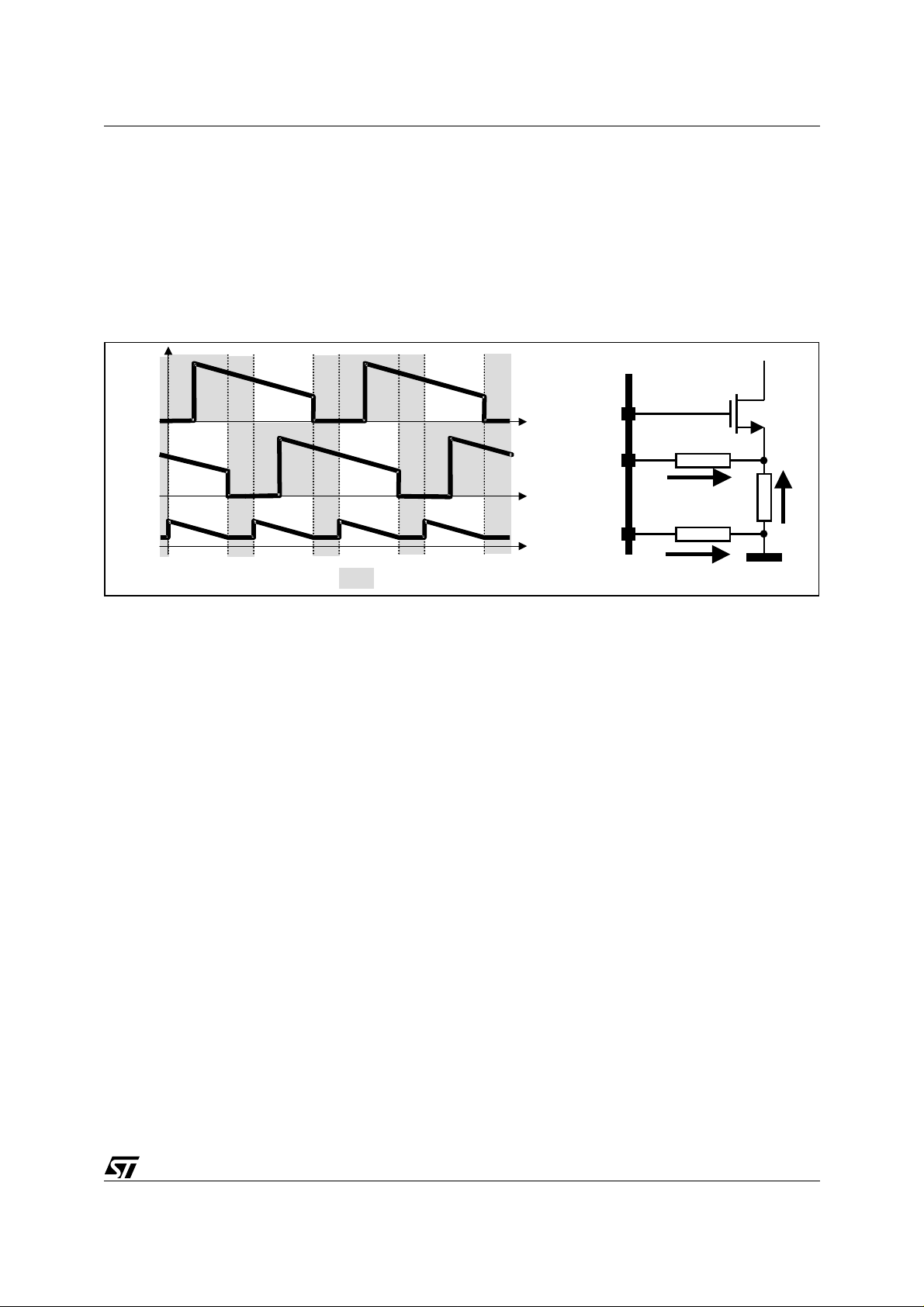
Soft Start and INHIBIT
At start-up a ramp is generated increasing the loop reference from 0V to the final value programmed by VID in
2048 clock periods as shown in figure 2.
Before soft start, the lower power MOS are turned ON after that V
to discharge the output capacitor and to protect the load from high side mosfet failures. Once soft start begins,
the reference is increased; when it reaches the bottom of the oscillator triangular waveform (1V typ) also the
upper MOS begins to swi tch and the output volta ge star ts to increase w ith c losed l oop regulation.. At the end of
the digital soft start, the Power Good comparator is enabled and the PGOOD signal is then driven high (See fig.
2). The Under Voltage comparator enabled when the reference voltage reaches 0.8V.
The Soft-Start will not take place, if both V
ing normal operation, if any under-voltage is detected on one of the two supplies the device shuts down.
Forcing the OSC/INH/FAULT pin to a voltage lower than 0.8V the device enter in INHIBIT mode: all the power
mosfets are turned off until this condition is removed. When this pin is freed, the OSC/INH/FAULT pin reaches
the band-gap voltage and the soft start begins.
µ
A current generator up to 3.3V max); in this way, to program a logic "1" it is enough to leave
reaches 2V (independently by Vcc value)
CCDR
and VCCDR pins are not abov e their own turn- on thresholds. Dur-
CC
Figure 2. Soft Start
VIN=V
CCDR
V
LGATEx
V
OUT
PGOOD
Turn ON threshold
2V
t
t
t
2048 Clock Cycles
Timing Diagram Acquisition:
t
CH1 = PGOOD; CH2 = V
; CH4 = LGATEx
OUT
9/33

L6917B
Driver Section
The integrated high-current drivers allow using different types of power MOS (also multiple MOS to reduce the
RDSON), maintaining fast switching transition.
The drivers for the high-side mosfets use BOOTx pins for supply and PHASEx pins for return. The drivers for
the low-side mosfets use VCCDRV pin for supply and PGND pin for return. A minimum voltage of 4.6V at VCCDRV pin is required to start operations of the device.
The controller embodies a sophisticated anti-shoot- through system to minimize low side body diode conduction
time maintaining good efficiency saving the use of Schottky diodes. The dead time is reduced to few nanoseconds assuring that high-side and low-side mosfets are never switched on simultaneously: when the high-side
mosfet turns off, the voltage on its source begins to fall; when the voltage reach es 2V, the low-side mosfet gate
drive is applied with 30ns delay. When the low-side mosfet turns off, the voltage at LGATEx pin is sensed. When
it drops below 1V, the high-side mosfet gate drive is applied with a delay of 30ns. If the current flowing in the
inductor is negativ e, the sourc e of high -side mos f et will nev er dr op. To all ow the tur ning on of the l ow-side mosfet even in this case, a watchdog controller is enabled: if the source of the high-side mosfet don't drop for more
than 240ns, the low side mosfet is switched on so allowing the negative current of the inductor to recirculate.
This mechanism allows the system to regulate even if the current is negative.
The BOOTx and VCCDR pins are separated from IC's power supply (VCC pin) as well as signal ground (SGND
pin) and power ground (PGND pin) in order to maximize the switching noise immunity. The separated supply
for the diff erent drivers gives high flexibility in mosfet choice, allow ing the use of logic- level mosf et. Several combination of supply can be chosen to optimize performance and efficiency of the application. Power conversion
is also flexible, 5V or 12V bus can be chosen freely.
The peak current is shown for both the upper and the lower driver of the two phases in figure 3. A 10nF capacitive load has been used. For the upper drivers, the source current is 1.9A while the sink current is 1.5A with
V
BOOT-VPHASE
VCCDR = 1 2V.
= 12V; similarly, for the lower drivers , the s our ce c urrent is 2.4A while the sink cur rent is 2A w ith
Figure 3. Drivers peak current: High Side (left) and Low Side (right)
CH3 = HGATE1; CH4 = HGATE2 CH3 = LGATE1; CH4 = LGATE2
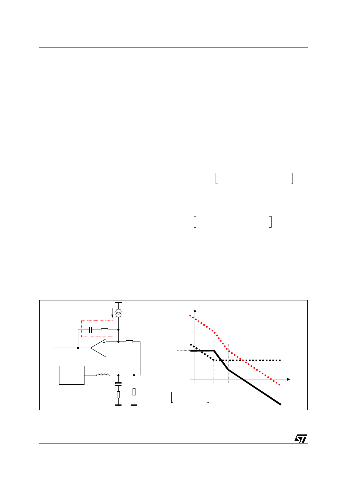
Current Reading and Over Current
The current flowing trough each phase is read using the voltage drop across the low side mosfets r
across a sense resistor (R
) and internally converted into a current. The transconductance ratio is issued
SENSE
DSON
or
by the external resistor Rg placed outsi de the chip between ISENx and PGNDSx pins toward the reading points.
The full differential current readi ng rejects noi se and allow s to plac e sensing el ement in different lo cations w ithout affecting the measurement's accuracy. The current reading circuitry reads the current during the time in
10/33
L6917B
which the low-side mosfet is on (OFF Time). During this time, the reaction keeps the pin ISENx and PGNDSx
at the same voltage while during the time in which th e reading circ uitry is off, an internal clamp keeps these two
pins at the same voltage sinking from the ISENx pin the necessary current.
The proprietary current reading circuit allows a very precise and high bandwidth reading for both positive and
negative current. This circuit reproduces the current flowing through the sensing element using a high speed
Track & Hold transconductance amplifier. In particular, it reads the cur rent during the second half of the OFF
time reducing noise injection into the device due to the mosfet turn-on (See fig. 4). Track time must be at least
200ns to make proper reading of the delivered current.
Figure 4. Current Reading Timing (Left) and Circuit (Right)
I
LS1
LGATEX
I
ISENx
Rg
Rg
R
SENSE
PHASE
I
I
LS2
Total current
information
ISENX
PGNDSX
Track & Hold
50µµA
This circuit sources a constant 50µA current from the PGNDSx pin and keeps the pins ISENx and PGNDSx at
the same voltage. Referring to figure 4, the current that flows in the ISENx pin is then given by the following
equation:
R
⋅
+==
g
50µAI
INFOx
is the current car ried by each
PHASE
R
SENSEIPHASE
--------------------------------------- -------+
Where R
I
ISENx
is an external sense resi stor or the rds,on of the l ow side mosfet and Rg is the transconductance
SENSE
50µA
resistor used between ISE Nx and PGNDSx pins toward the readi ng points; I
phase and, in particular, the current measured in the middle of the oscillator period
The current information reproduced internally is represented by the second term of the previous equation as
follow:
R
⋅
g
R
SENSEIPHASE
I
INFOx
---------------------------------------- ------=
Since the current is read in differential mode, also negative current information is kept; this allow the device to
check for dangerous returning current between the two phases assuring the complete equalization between the
phase's currents.
From the current information of each phase, information about the total current delivered (I
and the average current for each phase (I
AVG
= (I
INFO1
+ I
)/2 ) is taken. I
INFO2
is then compared to I
INFOX
FB
= I
INFO1
+ I
INFO2
AVG
to give the correction to the PWM output in order to equalize the current carried by the two phases.
The transconductance resistor Rg has to be designed in order to have current information of 25
at full nominal load; the over current intervention threshold is set at 140% of the nominal (IINFOx = 35
According to t he above relationship, the limiti ng c urren t (I
) for each phase, which has to be placed at one half
LIM
µ
A per phase
µ
A).
of the total delivered maximum current, results:
I
LIM
⋅
35µARg
-------------------------- -=
R
SENSE
Rg
I
LIMRSENSE
------------------------------------ -=
35µA
⋅
An over current is detected when the current flow ing into the sense element is greater than 140% of the nominal
)
11/33

L6917B
p
f
1
Ton
MAXTOFF
+
-------------------------------------------=
current (I
until I
INFO
>35µA): the device enters in Quasi-Constant-Current operation. The low-side mosfets stays ON
INFOx
becomes lower than 35µA skipping clock cycles. The high side mosfets can be turned ON with a T
ON
imposed by the control loop at the next available clock cycle and the device work s in the usual way until another
OCP event is detected.
The device limits the bottom of the inductor current triangular waveform. So the average current delivered can
slightly increase also in Over Current conditi on since the current ripple increases. In fact, the ON time increases
due to the OFF time rise because of the current has to reach the 140% bottom. The worst-case condition is
when the duty cycle reaches its maximum value (d=75% internally limited). When this happens, the device
works in Constant Current and the output voltage decrease as the load increase. Crossing the UVP threshold
causes the device to latch (FAULT pin is driven high).
Figure 5 shows this working condition
Figure 5. Con s ta nt C urrent operat i on
I
TonMAX TonMAX
eak
I
MAX
140%
Vout
UVP
Inom I
OCPIMAX
Droop
effect
Iout
It can be observed that the peak current (Ipeak) is greater than the 140% but it can be determined as follow:
–
Where I
Ipeak 1.4 I
is the nominal current and Vout
NOM
VINVout
NOM
MIN
-------------------------------------- -
is the minimum output voltage (VID-40% as explained below).
MIN
⋅+⋅=
Ton
L
MAX
The device works in Constant-Current, and the output voltage decreases as the load increase, until the output
voltage reaches the under -voltage threshold (Vout
). When this threshold is crossed, all mosfets are turned
MIN
off, the FAULT pin is driven high and the device stops working. Cycle the power supply to restart operation.
The maximum average current during the Constant-Current behavior results:
I
MAX
1.4 I
NOM
Ipeak 1.4 I
-------------------------------------------------
⋅+⋅=
2
⋅–
NOM
2
In this particular situati on, the switching frequency result s reduced. The O N time is the max imum all owed (TonMAX) while the OFF time depends on the application:
T
OFF
Over current is set anyway when I
venient values for I
. Since the OCP intervention threshold is fixed, to modify the percentage w ith respect to
FB
Ipeak 1.4 I
-------------------------------------------------
⋅=
L
reaches 35µA. The full load value is only a convention to w ork with con-
INFO x
Vout
⋅–
NOM
the load value, it can be simply considered that, for example, to have on OCP threshold of 170%, this will correspond to I
= 35µA (IFB = 70µA). The full lo ad current will then correspond to I
INFOx
= 20.5µA (IFB = 41µA).
INFO x
12/33

L6917B
(a) (b)
Integrated Droop Function
The device uses a droop function to satisfy the requirements of high performance microprocessors, reducing
the size and the cost of the output capacitor.
This method "recovers" part of the drop due to the output capacitor ESR in the load transient, introducing a dependence of the output voltage on the load current
As shown in figure 6, the ESR drop is pr esent in any c ase, but using the droop func tion the total deviation of the
output voltage is minimized. In practice the droop function introduces a static error (Vdroop in figure 6) proportional to the output c urrent. Si nce the devic e has an average c ur rent mode regulation, the information about the
total current delivered is used to implement the Droop Function. This current (equal to the sum of both I
is sourced from the FB pin. Connecting a resistor between this pin and Vout, the total current information flows
only in this resi stor becaus e the compensation networ k between FB and COMP has al ways a capac itor in series
(See fig. 7). The voltage regulated is then equal to:
V
= VID - RFB · I
OUT
FB
Since IFB depends on the current information about the two phases, the output characterist ic vs . load current is
given by:
R
SENSE
----------------------
V
OUT
VID R
FB
⋅⋅–=
Rg
I
OUT
Figure 6. Output transient response without (a) and with (b) the droop function
ESR DROP ESR DROP
INFOx
)
MAX
V
V
NOM
V
MIN
Figure 7. Active Droop Function Circuit
R
FB
COMP FB
V
PROG
The feedback current is equal to 50µA at nominal full load (IFB = I
so the maximum output voltage deviation is equal to:
I
FB
INFO 1
To VOUT
+ I
INFO 2
V
DROOP
) and 70µA at the OC threshold,
∆
V
FULL_P O S ITIV E_LOAD
= +RFB · 50µA
∆
V
POSITIVE_OC_THRESHOLD
= +RFB · 70µA
Droop function is provided only for positive load; if negative load is applied, and then I
sunk from the FB pin. The device regulates at the voltage programmed by the VID.
< 0, no current is
INFOx
13/33

L6917B
Output Voltage Protection and Power Good
The output voltage is monitored by pin VSEN. If it is not within +12/-10% (typ.) of the programmed value, the
powergood output is forced low. Power good is an open drain output and it is enabled only after the soft start is
finished (2048 clock cycles after start-up).
The device provides over voltage protection; when the voltage sensed by the V
controller permanently swi tches on both the low -side mos fets and sw itches off both the hi gh-side mosfe ts in or der to protect the CPU. The OSC/INH/FAULT pin is driven high (5V) and power supply (Vcc) turn off and on is
required to restart operations. The over Voltage percentage is set by the ratio between the OVP threshold (set
at 2.1V) and the reference programmed by VID.
pin reaches 2.1V (typ.), the
SEN
OVP[%]
---------------------------------------------------------------------------- -
Reference Voltage VID
2.1V
⋅=
()
100
Under voltage protection is also provided. If the output voltage drops below the 60% of the reference voltage for
more than one clock period the device turns off and the FAULT pin is driven high.
Both Over Voltage and U nder Voltage are active also during soft start (Under Voltage after than Vout reaches
0.8V). During soft-star t the reference voltage used to determine the OV and UV thresholds is the incr easing voltage driven by the 2048 soft start digital counter.
Remote Voltage Sense
A remote sense buffer is integrated into the dev ice to allow output voltage remo te sense implementation without
any additional external components. In this way, the output voltage programmed is regulated between the remote buffer inputs compensating motherboard trace losses or connector losses if the device is used for a VRM
module. The very low offset amplifier senses the output voltage remotely through the pins FBR and FBG (FBR
is for the regulated voltage sense while FBG is for the ground sense) and reports this voltage internall y at VSEN
pin with unity gain eliminating the errors.
If remote sense i s not requir ed, the output v oltage is s ensed by the VSEN pin c onnecting it di rectly to the output
voltage. In this case the FBG and FBR pins must be connected anyway to the regulated voltage.
Input Capacitor
The input capacitor is designed considering mainly the input rms current that depends on the duty cycle as reported in figure 8. Considering the dual-phase topology, the input rms current is highly reduced compar ing with
a single phase operation.
Figure 8. Input rms Current vs. Duty Cycle (D) and Driving Relationships
)
OUT
/I
RMS
0.50
0.25
Rms Current Normalized (I
Duty Cycle (V
Single Phase
Dual Phase
0.50 0.75 0.25
OUT/VIN
I
OUT
2
=
I
rms
)
I
OUT
2
<−⋅⋅
5.0DifD)2(12D
>−⋅⋅
0.5DifD)2(21)-(2D
It can be observed that the input rms value is one half of the single-phase equivalent input current in the worst
case condition that happens for D = 0.25 and D = 0.75.
14/33

The power dissipated by the input capacitance is then equal to:
L6917B
P
RMS
⋅=
ESR I
()
2
RMS
Input capacitor is designed in order to sustain the ripple relative to the maximum load duty cycle. To reach the
high rms value needed by the CPU power supply application and also to minimize components cost, the input
capacitance is realized by more than one physical capacitor. The equivalent rms current is simply the sum of
the single capacitor's rms current.
Input bulk capacitor must be equally divided between high-side drain mosfets and placed as close as possible
to reduce switching noise above all during load transient. Cerami c capacitor can also intr oduc e benefits in high
frequency noise decoupling, noise generated by parasitic components along power path.
Output Capacitor
Since the microprocessors require a current variation beyond 50A doing load transients, with a slope in the
µ
range of tenth A/
s, the output capacitor is a basic component for the fast response of the power supply.
Dual phase topology reduces the amount of output capacitance needed because of faster load transient response (switching frequency is doubled at the load connections). Current ripple cancellation due to the 180°
phase shift between the two phases also reduces requirements on the output ESR to sustai n a specified v oltage
ripple.
When a load transient is applied to the converter's output, for first few microseconds the current to the load is
supplied by the output capacitors. The controller recognizes immediately the load transient and increases the
duty cycle, but the current slope is limited by the inductor value.
The output voltage has a first drop due to the current variation inside the capacitor (neglecting the effect of the
ESL):
∆
V
OUT
= ∆I
OUT
· ESR
A minimum capacitor value is required to sustain the current during the load transient without discharge it. The
voltage drop due to the output capacitor discharge is given by the following equation:
2
∆
⋅
L
I
OUT
–⋅()⋅⋅
Where D
∆
V
OUT
is the maximum duty cycle value. The lower is the ESR, the lower is the output drop during load
MAX
---------------------------------------------------------------------------------------------=
2C
OUTVINMINDMAXVOUT
transient and the lower is the output voltage static ripple.
Inductor design
The inductance value is defined by a compromise between the transient response time, the efficiency, the cost
and the size. The inductor has to be calculated to sustain the output and the input voltage variation to maintain
the ripple current
∆
IL between 20% and 30% of the maximum output current. The inductance value can be cal-
culated with this relationship:
Where f
L
is the switching frequency, VIN is the input voltage and V
SW
∆⋅
fs I
–
V
INVOUT
------------------------------
V
OUT
-------------- -⋅=
V
L
IN
is the output voltage.
OUT
Increasing the value of the inductance reduces the ripple current but, at the same time, reduces the converter
response time to a load transient. The response time is the time required by the inductor to change its current
from initial to final value. Since the inductor has not finished its charging time, the output current is supplied by
the output capacitors. Minimizing the response time can minimize the output capacitance required.
The response time to a load transient is different for the application or the removal of the load: if during the application of the loa d the inductor is c harged by a voltage equal to the difference between the input and the output
15/33

L6917B
voltage, during the removal it is discharged only by the output voltage. The following expressions give approximate response time for
∆
I load transient in case of enough fast compensation network response:
t
applicatio n
∆⋅
LI
------------------------------=
–
V
INVOUT
t
removal
∆⋅
LI
-------------- -=
V
OUT
The worst condition depends on the input voltage available and the output voltage selected. Anyway the worst
case is the response ti me after r emoval o f the load with the minimum output voltage programmed and the maximum input voltage available.
Figure 9. Indu ct or ri pp le current vs V
out
9
8
7
6
5
4
3
Inductor Ripple [A]
2
1
0
0.5 1.5 2.5 3.5
L=1.5µH, Vin=12V
L=3µH, Vin=5V
Output Voltage [V]
L=2µH,
Vin=12V
L=3µH,
Vin=12V
L=1.5µH,
Vin=5V
L=2µH,
Vin=5V
MAIN CONTROL LOOP
The L6917B control loop is composed by the Current Sharing control loop and the Average Current Mode control loop. Each loop gives, with a proper gain, the correction to the PWM in order to minimize the error in its
regulation: the Current Sharing control loop equalize the currents in the inductors while the Average Current
Mode control loop fixes the output voltage equal to the reference programmed by VID. Figure 10 reports the
block diagram of the main control loop.
Figure 10. Main Control Loop Diagram
+
+
D02IN1392
16/33
PWM1
1/5
1/5
PWM2
ERROR
AMPLIFIER
4/5
CURRENT
SHARING
DUTY CYCLE
CORRECTION
PROGRAMMED
+
-
Z
F(S)
REFERENCE
BY VID
FBCOMP
Z
FB
I
INFO2
I
INFO1
L
1
L
2
C
O
R
O

L6917B
■
Current Sharing (CS) Control Loop
Active current sharing is implemented using the information from Tran conductance differential amplifier in an
average current mode control scheme. A current reference equal to the average of the read current (I
internally built; the error betw een the read current and this reference is converted to a volta ge with a proper gain
and it is used to adjust the duty cycle whose dominant value is set by the error amplifier at COMP pin (See fig.
11).
The current sharing control is a high bandwidth control loop allowing current sharing even during load transients.
The current sharing error is affected by the choice of external components; choose precise Rg resistor (±1% is
necessary) to sense the current. The current sharing error is internally dominated by the voltage offset of Tran
conductance differential amplifie r; consider ing a voltage offset equal to 2mV across the sense r esis tor, the current reading error is given by the following equation:
∆
Where
∆
I
is the difference between one phase current and the ideal current (I
READ
For Rsense = 4m
I
READ
------------------- -
I
MAX
Ω
and Imax = 40A the current sharing error is equal to 2.5%, neglecting errors due to Rg and
2mV
--------------------------------------- -=
R
SENSEIMAX
⋅
MAX
/2).
Rsense mismatches.
Figure 11. Current Shari n g C ontrol Loop
L
+
PWM1
1
AVG
) is
I
1/5
1/5
+
COMP
■
Average Current Mode (ACM) Control Loop
PWM2
CURRENT
SHARING
DUTY CYCLE
CORRECTION
D02IN1393
INFO2
I
INFO1
L
2
V
OUT
The average current mode control loop is reported in figure 12. The current information IFB sourced by the FB
pin flows into RFB implementing the dependence of the output voltage from the read current.
The ACM control loop gain results (obtained opening the loop after the COMP pin):
G
LOOP
()
s
PWM Z
--------------------------------------------------------------------------------------------------------------------=
()
Z
s
P
F
()+()
ZLs
s()R
DROOPZP
()
s
Z
F
-------------- -
As
1
()
1
----------- -+
()
As
()+()⋅⋅
s
⋅+⋅
R
FB
Where:
R
sense
– is the equivalent output resistance determined by the droop function;
R
DROOP
------------------ -
R
⋅=
R
FB
g
–Z
(s) is the impedance resulting by the parallel of the output capacitor (and its ESR) and the applied
P
load Ro;
17/33
L6917B
–ZF(s) is the compensation network impedance;
(s) is the parallel of the two inductor impedance;
–Z
L
– A(s) is the error amplifier gain;
∆
V
4
– · is the ACM PWM transfer function where DVosc is the oscillator ramp amplitude
PWM
-- -
5
and has a typical value of 2V
Removing the dependence from the Error Amplifier gain, so assuming this gain high enough, the control loop
gain results:
With further simplifications, it results:
LOOP
()
s
G
------------------ -
⋅=
∆
V
4
-- -
5
IN
OSC
------------------ -
⋅⋅⋅ ⋅–=
∆
V
V
G
LOOP
IN
OSC
()
s
()
Z
F
-------------- -
R
FB
4
⋅⋅ ⋅–=
-- -
5
s
+
Ro R
------------------------------------- -
Ro
V
IN
------------------ -
∆
V
OSC
DROOP
R
------ -+
2
()
s
Z
F
----------------------------------- -
s()ZLs
Z
P
Rs
------- -
()+
Rg
1sCoR
----------------------------------------------------------------------------------------------------------------------------------
L
2
s
Co
L
-- -
s
2
Z
P
---------------+
R
DROOP
L
---------------
⋅
2Ro
()
s
FB
+()⋅⋅+
//Ro ESR
Co ESR Co
R
L
------ -
⋅+⋅+
+⋅+⋅⋅
1
2
Considering now that in the application of interest it can be assumed that Ro>>R
R
<<Ro, it results:
DROOP
LOOP
()
s
G
4
-- -
5
V
------------------ -
⋅⋅⋅–=
∆
V
IN
OSC
()
s
Z
F
-------------- -
R
FB
+()⋅⋅+
----------------------------------------------------------------------------------------------------------------------------------
1sCoR
2
s
Co
L
---
2
s
---------------
2Ro
⋅
DROOP
L
Co ESR Co
ESR
; ESR<<Ro and
L
R
L
------ -⋅+⋅+
+⋅+⋅⋅
1
2
The ACM control loop gai n is designed to obtain a high D C gain to m inimiz e static er ror and cr os s the 0dB ax es
with a constant -20dB/dec slope with the desired crossover frequency
ω
. Neglecting the effect of ZF(s), the
T
transfer function has one zero and two poles. Both the poles ar e fixed once the output filter is des igned and the
zero is fixed by ESR and the Droop resi stance. To obtain the de sir ed shape an R
ered for the Z
(s) implementation. A zero at
F
ω
=1/RFCF is then introduced together with an integrator. This in-
F
series network is co nsid-
F-CF
tegrator minimizes the static error while placing the zero in correspondence with the L-C resonance a simple 20dB/dec shape of the gain is assured (See Figure 12). In fact, considering the usual value for the output filter,
the LC resonance results to be at frequency lower than the above reported zero.
Figure 12. ACM Control Loop Gain Block Diagram (left) and Bode Diagram (right)
dB
G
LOOP
K
ZF(s)
V
COMP
I
FB
F
Z
C
F
R
F
R
FB
REF
PWM
d•V
IN
Cout
ESR
V
OUT
Rout
K
=
L/2
Compensation network can be s imply designed placing
desired obtaining:
18/33
V
4
IN
---------------
-- -
⋅⋅
5
∆
ω
Z
----------
R
V
osc
ω
=
and imposing the cross-ov er frequency
LC
1
FB
dB
ω
ω
Z
LC
ω
T
ω
ω
as
T

L6917B
C
F
Co
L
2
-- -
⋅
R
F
------------------- -=
∆⋅
R
F
R
FBVOSC
----------------------------------
V
IN
------------------------------------------------------- -
⋅⋅ ⋅=
ω
T
2R
L
DROOP
+()⋅
ESR
LAYOUT GUIDE LINES
Since the device manages control functions and high -current driv ers, layout is one of the most imp ortan t things
to consider when designing such high current applications.
A good layout solution can generate a benefit in lowering power dissipation on the power paths, reducing radiation and a proper connection between signal and power ground can optimise the performance of the control
loops.
Integrated power drivers reduc e components count and interconnec tions between control fun ctions and drivers,
reducing the board space.
Here below are listed the main points to focus on when starting a new layout and r ules are suggested for a correct implementation.
■
Power Connections.
These are the c onnections wher e switching and continuous current fl ows from the input supp ly towards the load.
The first priority when placing components has to be reserved to this power section, minimizing the length of
each connection as much as possible.
To minimize noise and vol tage spikes (EMI and l osses) these interconnections must be a part of a pow er plane
and anyway realized by wi de and thick copper traces. The critical components, i.e. the power transistors, must
be located as close as possible, together and to the controller. Considering that the "electrical" components reported in fig. 13 are composed by more than one "physical" component, a ground plane or "star" grounding connection is suggested to minimize effects due to multiple connections.
5
-- -
4
Figure 13. Power connections and related connections layou t guidel ines (same for bo th phases)
VIN
L
C
D
CIN
OUT
LOAD
HGATEx
PHASEx
LGATEx
PGNDx
HS
R
gat e
LS
R
gat e
a. PCB power and ground planes areas b. PCB small signal components placement
PHASEx
SGND
BOOTx
VCC
C
BOOTx
+VCC
HS
LS
C
VCC
VIN
L
C
D
CIN
OUT
LOAD
Fig. 13a shows the details of the power connections involved and the current loops. The input capacitance
(CIN), or at least a portion of the total capaci t ance needed, has to be pl aced clos e to the power sect ion in order
to eliminate the stray inductance generated by the copper traces. Low ESR and ESL capacitors (electrolytic or
Ceramic or both) are required.
■
Power Connections Relat ed.
Fig.13b shows some small signal components placement, and how and where to mix signal and power ground
planes.
The distance from drivers and mosfet gates should be reduced as much as possible. Propagation delay times
19/33

L6917B
as well as for the voltage spikes generated by the distributed inductance along the copper traces are so minimized.
In fact, the further the mosfet is from the device, the longer is the interconnecting gate trace and as a consequence, the higher are the voltage spi kes corres ponding to the gate pwm rising and fall ing signals. E ven if these
spikes are clamped by inherent internal diodes, propagation delays, noise and potential causes of instabilities
are introduced jeopardizing good system behavi or. One important consequence is that t he switching losses for
the high side mosfet are significantly increased.
For this reason, it is suggested to have the device oriented with the driver side towards the mosfets and the
GATEx and PHASEx traces walking together toward the high side mosfet in or der to minimi ze distanc e (see fig
14). In addition, since the PHASEx pin is the return path for the high side driver, this pin must be connected
directly to the High Side mosfet Source pin to have a proper driving for this mosfet. For the LS mosfets, the return path is the PGN D pin: it can be connected directly to the power ground plane (if implemented) or in the
same way to the LS mosfets Source pin. G ATEx and PHASEx connections (and also PGND when no power
ground plane is implemented) must also be designed to handle current peaks in excess of 2A (30 mils wide is
suggested).
Gate resistors of few ohms help in reducing the power dissipated by the IC without compromising the system
efficiency.
Figure 14. Device orientation (left) and sense nets routing (right)
To LS mosfet
Towards HS mosfet
(30 mils wide)
(or sense resist or)
Towards LS mosfet
(30 mils wide)
Towards HS mosfet
(30 mils wide)
To LS mosfet
(or sense resist or)
To regulated output
The placement of other components is also important:
– The bootstrap capacitor must be placed as close as possib le to the BOOT x and PHASEx pins to mini-
mize the loop that is created.
– Decoupling capacitor from Vcc and SGND placed as close as possible to the involved pins.
– Decoupling capacitor from VCCDR and PGND placed as close as possible to t hose pins. This capaci tor
sustains the peak currents requested by the low-side mosfet drivers.
– Refer to SGND all the sensible components such as frequency set-up resistor (when present) and also
the optional resistor from FB to GND used to give the positive droop effect.
– Connect SGND to PGND on the load side (output capacitor) to avoid undesirable load regulation effect
and to ensure the right precision to the regulation when the remote sense buffer is not used.
– An additional 100nF ceramic capacitor is suggested to place near HS mosfet drain. This helps in reduc-
ing noise.
– PHASE pin spikes. Since the HS mosfet switches in hard mode, heavy voltage spikes can be observed
on the PHASE pins. If these voltage spikes overcome the max breakdown voltage of the pin, the device
can absorb energy and it can cause damages. The voltage spikes must be limited by proper layout, the
use of gate resistors, Schottky diodes in parallel to the low side mosfets and/or snubber network on the
low side mosfets, to a value lower than 26V, for 20nSec, at Fosc of 600kHz max.
■
Current S ens e Connectio ns .
Remote Buffer:
The input connections for this component must be routed as parallel nets from the FBG/FBR
20/33

L6917B
pins to the load in order to compensate losses along the output power traces and also to avoid the pick-up of
any common mode noise. Connecting these pins in poin ts far from the load will cause a non- optimum load regulation, increasing output tolerance.
Current Reading:
order to limit the noise injection into the device. The PCB traces connecting these resistors to the reading point
must be routed as parallel traces in order to avoid the pick-up of any common mode noise. It's also important
to avoid any offset in the measurement and to get a better precision, to connect the traces as cl ose as possi ble
to the sensing elements, dedicated current sense resistor or low side mosfet Rdson.
Moreover, when using the low side mosfet RdsON as current sense element, the IS ENx pin is practically connected to the PHAS Ex pin. DO N OT CONNEC T THE PIN S TOGETHER AND TH EN TO THE H S SOURC E!
The device won't work properly because of the noise generated by the return of the high side driver. In this case
route two separate nets: connect the PHASEx pin to the HS Source (route together with HGATEx) with a wide
net (30 mils) and the ISENx pin to the LS Drain (route together with PGNDSx). Moreover, the PGNDSx pin is
always connected, through the R g resistor, to the PGND: DO NOT CONNECT DIRECTLY TO THE PGND! In
this case, the device won't work properly. Route anyway to the LS mosfet source (together with ISENx net).
Right and wrong connections are reported in Figure 15.
Symmetrical layout is also suggested to avoid any unbalance between the two phases of the converter.
Figure 15. PCB layout connections for sense nets
The Rg resistor has to be placed as close as possible to the ISENx and PGNDSx pins in
NOT CORRECT
VIA to GND plane
ToPHASE
connection
Wrong (left) and correct (right) connections for the current reading sensing nets.
CORRECT
To LS Drai n
and Source
To HS Gate
and Source
APPLICATION EX AMPLES
The dual-pahse topology can be applied to several different applications ranging from CPU power supply (for
which the device has been designed) to standard high current DC-DC power supply. The application benefits
of all the advantages due to the dual-phase topology ranging from output ripple reduction to dynamic performance increase. After a general demo board overview, the following application examples will be illustrated:
– CPU Power Supply: 5 to 12 VIN; 1.7V
– CPU Power Supply: 12V
– High Current DC-DC: 12V
; VRM 9.0 Output; 50A
IN
; 3. 3 to 5V
IN
OUT
OUT
; 45A
T; 35A
Demo Board Description
The demo board shows the operation of the device in a dual phase application. This evaluation board allows
output voltage adjustability (1.100V - 1.850V) through the switches S0-S4 and high output current capability.
2
The board has been laid out with the possi bility to use up to two D
PACK mosfets for the low side sw itch in order
to give maximum flexibility in the mosfet's choice.
The four layers demo boar d's copper thickness is of 70
µ
m in order to minimize conduction losses considering
the high current that the circuit is able to deliver.
Demo board schematic circuit is reported in Figure 16.
21/33

L6917B
G
Figure 16. Demo Board Schematic
Vin
GNDin
Vcc
GNDcc
JP6
S4
S3
S2
S1
S0
DZ1
JP1
C5
L1
D4
Q2
C4
D1
Q1
Q1a
JP2
R16
C8
R15
R18
R13
R6
R5
R2
VCCDR
BOOT1
UGATE1
PHASE1
LGATE1
ISEN1
PGNDS1
OSC / I NH
SGND
VID4
VID3
VID2
VID1
VID0
2
5
4
3
1
13
14
L6917B
22
21
20
19
18
17
7
11
FBR
U1
C11..C13
R10
VCC
6
24
25
26
27
16
15
28
23
10
9
8
12
FBG
BOOT2
UGATE2
PHASE2
LGATE2
ISEN2
PGNDS2
PGND
PGOOD
VSEN
FB
COMP
C7
R14
R17
R12
R3
D3
Q4 C3
Q3
Q3a
C6
L2
D2
R4
R7
R8
C2
JP3
C1
R9
C9,C10
C14,
C23
R1
R19
R20
JP4
VoutCORE
GNDCORE
PGOOD
JP5
FBG
FBR
Several jumpers allow setting different configurations for the device: JP3, JP4 and JP5 allow configuring the
remote buffer as desired. Simply shorting JP4 and JP5 the remote buffer is enabled and it senses the output
voltage on-board; to implement a real remote sense, leave these jumpers open and connect the FBG and FBR
connectors on the demo board to the remote load. To avoid usi ng the remote buffer, simpl y short all the j umpers
JP3, JP4 and JP5. Local sense through the R7 is used for the regulation.
The input can be configured in different ways using the jumpers JP1, JP2 and JP6; these jumpers control also
the mosfet driver supply voltage. Anyway, power conversion starts from VIN and the device is supplied from
V
(See Figure 17).
CC
Figure 17. Power supply conf i gu ra ti on
Vin
NDin
Vcc
GNDcc
To Vcc pin
JP6
DZ1
JP1
JP2
To HS Drains ( Po wer Input)
To BOOTx (HS Driver Supply)
To VCCDR pin (LS Driver Supply)
Two main configur ations can be di stinguis hed: S ingle Supply ( VCC = VIN = 12V) and Double Supply (VCC = 12V
= 5V or different).
V
IN
22/33

L6917B
V
– Single Supply: In this case JP6 has to be completely shorted. The device is supplied with the same rail
that is used for the conversion. With an additional zener diode DZ1 a lo wer voltage can be derived to
supply the mosfets driver if Logic level mosf et are us ed. In this c ase J P1 must be left op en so th at the
HS driver is supplied with V
the right to use V
IN-VDZ1
IN-VDZ1
to supply the LS driver through VCCDR pin. Otherwise, JP1 must be shorted
and JP2 can be freely shorted in one of the two positions.
– Double Supply: In this case V
the power conversion. This la st one can start ind ifferently from the 5 V bus (Typ.) or from other buses
allowing maximum flexibility in the power conversion. Supply for the mosfet driver can be programmed
through the jumpers JP1, JP2 and JP6 as previously illustrated. JP6 selects now V
on the requirements.
Some examples are reported in the following Figures 18 and 19.
Figure 18. Jumpers configuration: Double Supply
through BOOTx and JP2 must be shorted to the left to use VIN or to
supply directly the controller (12V) while VIN supplies the HS drains for
CC
or VIN depending
CC
Vcc = 12V
Vin = 5V
Vcc = 12V
GNDin
GNDcc
JP6
(a) VCC = 12V; V
DZ1
BOOTx
JP2
JP1
= VCCDR = VIN = 5V (b) V
HS Drains = 5V
HS Supply = 5V
VCCDR (LS Supply) = 5V
Figure 19. Jumpers configuration: Single Supply
Vcc = 12V
Vin = 12V
GNDin
Vcc = Open
GNDcc
JP6
DZ1 6.8V
JP2
JP1
(a) VCC = VIN = VCCDR = 12V; V
HS Drains = 12V
HS Supply = 5.2V
VCCDR (LS Supply) = 12V
= 5.2V (b) VCC = VIN= V
BOOTx
Vcc = Open
Vin = 5V
GNDin
Vcc = 12V
GNDcc
Vin = 12V
GNDin
GNDcc
Vcc = 12V
JP6
DZ1
JP1
HS Drains = 5V
HS Supply = 12V
JP2
VCCDR (LS Supply) = 12
= V
CC
JP6
= VCCDR =12V; V
BOOTx
DZ1
JP1
Vcc = 12V
HS Drains = 12V
HS Supply = 12V
JP2
VCCDR (LS Supply) = 12V
IN
= 5V
= VCCDR = 12V
BOOTx
23/33

L6917B
PCB and Components Layouts
Figure 20. PCB and Components Layouts
Component Side Internal PGND Plane
Figure 21. PCB and Components Layouts
24/33
Internal SGND Plane Solder Side

L6917B
CPU Power Supply: 5 to 12VIN; 1.7V
OUT
; 45A
Considering the high slope for the load transient, a high switching frequency has to be used. In addition to fast
reaction, this helps in reducing output and input capacitor. Inductance value is also reduced.
A switching frequency of 200kH z for each phase is then considered allowing large bandwidth for the compensation network. It can be considered to use the 5V rail for the power conversion in order to allow compatibility
with standard ATX power supply.
– Current Reading Network and Over Current:
Since the maximum output current is I
= 45A, the over current threshold has been set to 46A (23A
MAX
per phase) in the worst case (max mosfet temperature). This because the device limits the valley of the
triangular ripple across the inductors. Considering to sense the output current across the low-side mos-
fet RdsON, STB90NF03L ha s 6.5mΩ max at 25°C that becomes 9 .1mΩ considering the temperature
variation (+40%); the resulting Tran conductance resistor Rg has to be:
I
RdsON
MAX
------------ -
-------------------- -
(R3 to R6)
Rg
⋅
2
35
µ
46
------
9.1m
-------------
⋅
35
µ
2
Ω===
5.9k
– Droop function Design:
Considering a voltage drop of 100mv at full load, the feedback resistor RFB has to be:
100m V
FB
-------------------
70µA
R
1.43k
Ω==
(R7)
– Inductor design:
Each phase ha s to del iver up to 22.5A; conside ring a current ripple of 5A (<25 % ), the res ulting induc-
tance value is:
–
Vin Vout
---------------------------- -
== =
L
∆
l
-----------
⋅
Fsw
d
–
12 1.7
-------------------- -
5
1.7
------------------- -
------- -
⋅⋅
300000
12
1
µ
1
H
(L1, L2)
– Output Capacitor:
Five Rubycon MBZ (2200µF / 6.3V / 12mΩ max ESR) has been used implementing a resulting ESR of 2.4m
Ω
resulting in an ESR voltage drop of 45A*2.4mΩ = 108mV after a 45A load transient.
– Compensation Network:
A voltage loop bandwidth of 20kHz is considered to let the device fast react after load transient.
The R
R
F
network result s:
F CF
R
∆⋅
FBVOSC
== =
----------------------------------
V
IN
5
ω
⋅⋅ ⋅
-- -
-------------------------------------------------------
T
4
2R
Co
------------------- -
== =
C
(C2)
F
R
L
()⋅
DROOP
L
-- -
⋅
2
F
ESR
+
⋅⋅
62200
---------------------------------------- -
6.2k
1.43k 2⋅
----------------------
12
µ
1
------ -
µ
2
5
20k 2π
⋅⋅ ⋅ ⋅ 6200Ω
-- -
4
------------------------------------------------------------------ -
2
⋅
15nF
9.1m
-------------
5.9k
1µ
1.43k 2.4m
⋅
+
(R8)
25/33

L6917B
Part List
R1 10k SMD 0805
R2, R20 Not Mounted SMD 0805
R3, R4, R5, R6 5.1k 1% SMD 0805
R7 1.43k 1% SMD 0805
R8 6.2k SMD 0805
R10 82Ω SMD 0805
R12 to R16, R19 2.2Ω SMD 0805
R17, R18 0Ω SMD 0805
C2 15n SMD 0805
C3, C4 100n SMD 0805
C5, C6, C7 1µ Ceramic SMD 1206
C8, C9, C10 10µ Ceramic SMD 1206
C11, C12, C13 1800µ / 16V Rubycon MBZ Radial 23x10.5
C19 to C24 2200µ / 6.3V Rubycon MBZ Radial 23x10.5
L1, L2 1µ TO50 – 52B – 6 Turns
U1 L6917B STMicroelectronics SO28
Q1, Q3 STB90NF03L STMicroelectronics
Q2, Q4 STB70NF03L STMicroelectronics
D1, D2 STPS340U STMicroelectronics SMB
D3, D4 1N4148 STMicroelectronics SOT23
D
D
2
PACK
2
PACK
System Efficiency
Figure 22 shows the demo board measured efficiency versus load current for different values of input voltage.
Mosfet temperature is always lower than 115 °C, at T
Figure 22. Efficiency (f
26/33
= 200kHz; Vout = 1.7V)
osc
95
90
85
80
75
70
65
60
Efficiency [%]
55
50
45
0 5 10 15 20 25 30 35 40
Output Current [A]
= 25°C.
amb
Vin= 12V
Vin=5V

L6917B
CPU Power Supply: 12VIN - VRM 9.0 - 50A thermal
Figure 23 shows the device in a high current CPU core power supply solution.
The output voltage can be adjusted with binary step from 1.100V to 1.850V following VRM 9.0 specifications.
The demo board assembled with the following part list is capable to deliver up to 50A in open air without any
kind of airflow. Peak current can reach 60A without any limitations. For higher DC current, to avoid mosfet
change, airflow or heat sink are required.
Figure 23. CPU Power Supply Sc hema t ic
Vin
GNDin
Vcc
GNDcc
JP6
S4
S3
S2
S1
S0
To Vcc Rosc
DZ1
JP1
C5
L1
D4
Q2
C4
Q1
D1
Q1a
JP2
R16
C8
R2
R15
R18
R13
VCCDR
R6
R5
2
BOOT1
5
UGATE1
4
PHASE1
3
LGATE1
1
ISEN1
13
14
L6917B
22
21
20
19
18
17
7
11
FBR
U1
PGNDS1
VID4
VID3
VID2
VID1
VID0
OSC / I NH
SGND
VCC
6
BOOT2
24
UGATE2
25
PHASE2
26
LGATE2
27
ISEN2
16
PGNDS2
15
PGND
28
PGOOD
23
VSEN
10
FB
9
COMP
8
12
FBG
R10
C7
R14
R17
R12
R3
D3
Q4 C3
Q3
Q3a
C6
L2
D2
R4
Ra
R7
R8
C2
JP3
Ca
C1
R9
C9,C10
C14,
C23
R1
C11..C13
R19
R20
JP4
VoutCORE
GNDCORE
PGOOD
JP5
FBG
FBR
Part List
R1 10k SMD 0805
R2, R9 Not Mounted SMD 0805
R3, R4, R5, R6 3.3k 1% SMD 0805
R7 3.6k 1% SMD 0805
R8 3.3k SMD 0805
R10 82 SMD 0805
R12 to R15 2.2 SMD 0805
R16, R17, R18 0 SMD 0805
Ra 1k SMD 0805
Rosc 1.3M 1% SMD 0805
C1 Not Mounted SMD 0805
27/33

L6917B
Part List
(continued)
C2 47n SMD 0805
C3, C4 100n Ceramic SMD 0805
C5, C6, C7, C8 1µ Ceramic SMD 1206
C9, C10 10µ Ceramic SMD 1206
C11 to C13 1800µ/ 16V Rubycon MBZ Radial 10x10.5
C14 to C23 2200µ/ 6.3V Rubycon MBZ Radial 10x10.5
Ca 68n SMD 0805
L1, L2 0.5µ 77121 Core – 3 Turns
U1 L6917B STMicroelectronics SO28
Q1,Q1a, Q3,Q3a SUB85N03-04P Vishay - Siliconix
Q2, Q4 SUB70N03-09BP Vishay - Siliconix
D
D
2
PACK
2
PACK
D1, D2 STPS340U STMicroelectronics SMB
D3, D4 1N4148 STMicroelectronics SOT23
Efficiency
Figure 24 showes the system efficiency for output current ranging form 5A up to 50A.
Figure 24. Efficiency (f
= 200kHz; Vout = 1.7V)
osc
89
87
85
83
81
Efficiency [%]
79
77
75
0 5 10 15 20 25 30 35 40 45 50 55
Output Current [A]
28/33
L6917B
Current Sharing
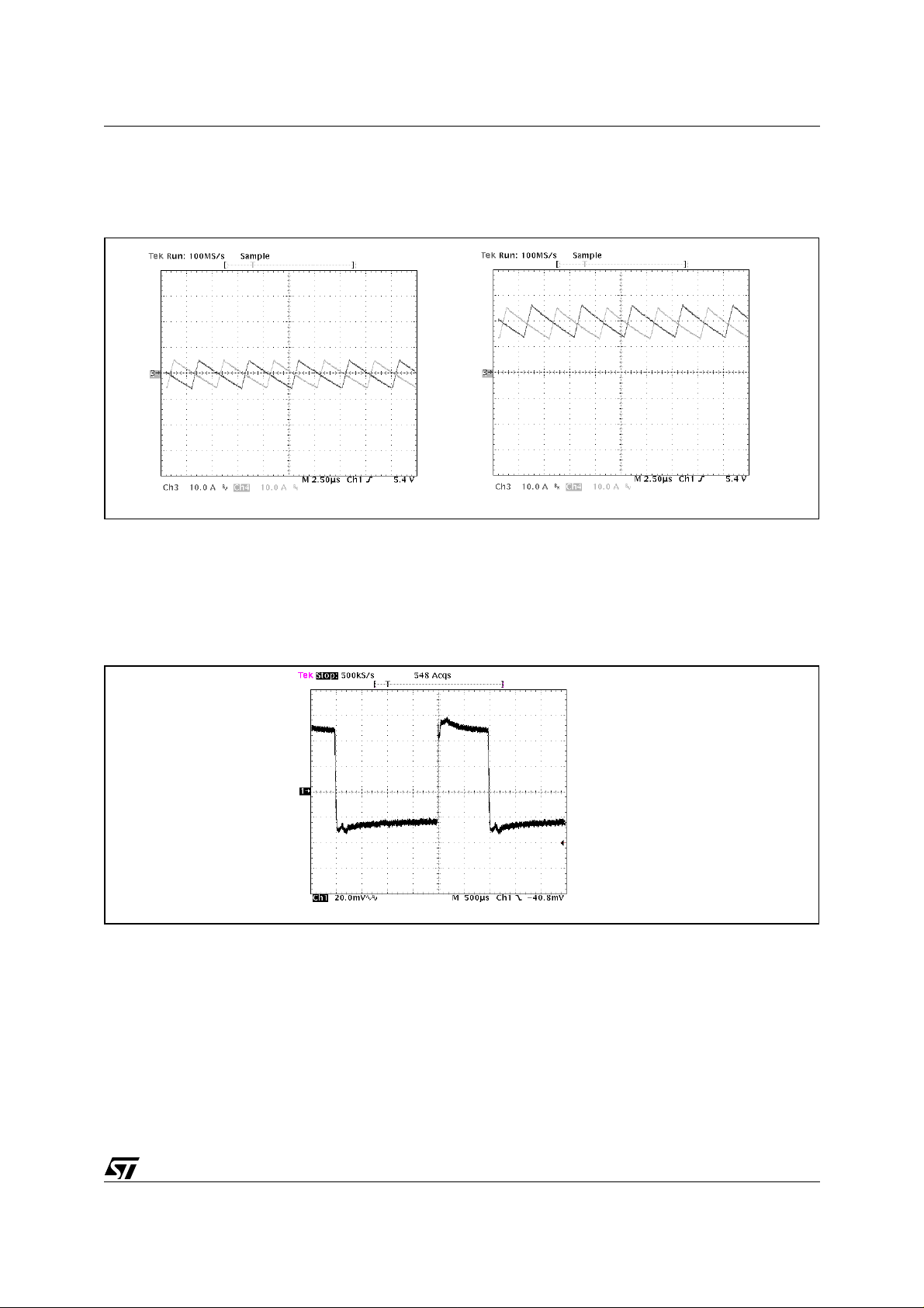
Figure 25 shows the current balancing between the two phases for different values of output current.
Figure 25.
Load Transient Response
Figure 26 shows the system response from 0 to 50A load transient. To obtain such a response, 5 additional
capacitors have been added to the output filter to reproduce the motherboard output filter. Noise can be further
reduced by adding ceramic decoupling capacitors.
Figure 26. 1.7V Output Voltage Ripple During 0 to 50A Load Transient
29/33

L6917B
High Current DC-DC: 12V
- 3.3 (or 5V) OUT - 35A
IN
Figure 27 shows the device in a high current server power supply application.
Adding an external resistor divider after the remote sense buffer gives the possibility to increase the regulated
voltage. Considering for example a divider by two (two equal resistors) the DAC range is doubled from 2.200V
to 3.700V with 50mV binary steps. The external resistor divider must be designed in order to give negligible effects to the remote buffer gain, this means that the resistors value must be much lower than the remote buffer
input resistance (20k
Ω
). In this way, it is possible to regulate the 3.3V and 2.5V rails from the 12V avail able from
the AC/DC converter. The 5V rail can be obtained with further modifications to the external divider. The regulator
assures all the advantages of the dual phase conversion especially in the 5V conversion where the duty cycle
is near the 50% and practically no ripple is present in the input capacitors.
The board is able to deliver up to 35A "thermal" at T
25°C without airflow. Higher currents can be reached
amb
for reasonable times considering the overall dynamic thermal capacitance.
Figure 27. Server power supply schematic
Vin
GNDin
Vcc
GNDcc
JP6
S4
S3
S2
S1
S0
To Vcc Rosc
DZ1
JP1
C5
L1
D4
Q2
C4
Q1
D1
Q1a
JP2
R16
R2
VCCDR
C8
R15
R18
R13
R6
R5
2
BOOT1
5
UGATE1
4
PHASE1
3
LGATE1
1
ISEN1
13
PGNDS1
VID4
VID3
VID2
VID1
VID0
OSC / INH
SGND
14
L6917B
22
21
20
19
18
17
7
11
FBR
U1
VCC
6
BOOT2
24
UGATE2
25
PHASE2
26
LGATE2
27
ISEN2
16
PGNDS2
15
PGND
28
PGOOD
23
VSEN
10
FB
9
COMP
8
12
FBG
R10
C7
R14
R17
R12
R3
D3
Q4 C3
Q3
Q3a
C6
L2
D2
R4
R7
R8
C2
JP3
C1
R9
C9,C10
C14,
C23
R1
C11..C1 3
R19
R20
JP4
VoutCORE
GNDCORE
PGOOD
JP5
FBG
FBR
The following part list refers to the following application:
– Input Voltage: 12V;
– Output voltage: 3.3V;
– Oscilator frequency: 200kHz;
– Output voltage tolerance (over static and dynamic conditions): ±2.5%.
30/33

Part List
]
R1 10k SMD 0805
R2, R9 Not Mounted SMD 0805
R3, R6 1.3k 1% SMD 0805
R4, R5 390 1% SMD 0805
R7 75 1% SMD 0805
R8 750 SMD 0805
R10 82 SMD 0805
R12 to R15 2.2 SMD 0805
R16, R17, R18 0 SMD 0805
R19 300 1% SMD 0805
R20 390 1% SMD 0805
R
OSC
C1 Not Mounted SMD 0805
C2 220n SMD 0805
C3, C4 100n Ceramic SMD 0805
C5, C6, C7, C8 1µ Ceramic SMD 1206
C9, C10 10µ Ceramic SMD 1206
C11 to C13 100µ/ 20V OSCON 20SA100M Radial 10x10.5
C14,C16,C18,C20,C22 2200µ/16V SANYO Radial 10x23
L1, L2
U1 L6917B STMicroelectronics SO28
Q1,Q1a,Q2, Q3,Q3a,Q4 STB90NF03L STMicroelectronics
D1, D2 STPS340U STMicroelectronics SMB
D3, D4 1N4148 STMicroelectronics SOT23
DZ1 Not Mounted Minimelf
1.3M 1% SMD 0805
µ 77121 Core – 9 Turns
2.8
2
PACK
D
L6917B
Figure 28. System Efficiency for a 12V/3.3V
Application (f
93
92
91
90
Efficiency [%
89
88
0 5 10 15 20 25 30 35 40
Output Current [A]
= 200kHz)
osc
Figure 29. Load Transient Response: 0A to 35A
@ 1A/µs
31/33

L6917B
DIM.
MIN. TYP. MAX. MIN. TYP. MAX.
A 2.65 0.104
a1 0.1 0.3 0.004 0.012
b 0.35 0.49 0.014 0.019
b1 0.23 0.32 0.009 0.013
C 0.5 0.020
c1 45° (typ.)
D 17.7 18.1 0.697 0.713
E 10 10.65 0.394 0.419
e 1.27 0.050
e3 16.51 0.65
F 7.4 7.6 0.291 0.299
L 0.4 1.27 0.016 0.050
S8° (max.)
mm inch
OUTLINE AND
MECHANICAL DATA
SO28
32/33

L6917B
Information furnished is believed to be accurate and reliable. However, STMicroelectronics assumes no responsibility for the consequences
of use of such information nor for any infringement of patents or other rights of third parties which may result from its use. No license is granted
by implic ation or otherwise under any patent or p at ent rights of STMicroelectronics. Spec i fications mentioned i n this publication are subject
to change without notice. This publication supersedes and replaces all information previously supplied. STMicroelectronics products are not
authorized for use as cri t i cal compone nts in life support device s or systems without express written approval of STMicroel ectronics.
The ST logo is a registered trademark of STMicroelectronics
2002 STMi croelectronics - All Ri ghts Rese rved
Australi a - Brazil - Chin a - Finland - Franc e - Germany - Hong Kong - India - Ita l y - Japan - Malaysi a - Malta - Morocco - Singapore - Spain
STMicroelectronics GROUP OF COMPANIES
- Sweden - Sw itzerlan d - United Kin gdom - U.S.A.
http://www.s t. com
33/33
 Loading...