


查询L6917DTR供应商查询L6917DTR供应商
5 BIT PROGRAMMABLE DUAL-PHASE CONTROLLER
■
2 PHASE OPERATION WITH
SYNCRHONOUS RECTIFIER CONTROL
■ ULTRA FAST LOAD TRANSIENT RESPONSE
■
INTEGRATED HIGH CURRENT GATE
DRIVERS: UP TO 2A GATE CURRENT
■
TTL-COMPATIBLE 5 BIT PROGRAMMABLE
OUTPUT COMPLIANT WITH VRM 9.0
■
0.8% INTERNAL REFERENCE ACCURACY
■
10% ACTIVE CURRENT SHARING
ACCURACY
■ DIGITAL 2048 STEP SOFT-START
■
OVERVOLTAGE PROTECTION
■
OVERCURRENT PROTECTION REALIZED
USING THE LOWER MOSFET’S R
SENSE RESISTOR
■
300 kHz INTERNAL OSCILLATOR
■
OSCILLATOR EXTERNALLY ADJUSTABLE
UP TO 1MHz
■ POWER GOOD OUTPUT AND INHIBIT
FUNCTION
■
REMOTE SENSE BUFFER
■ PACKAGE: SO-28
APPLICATIONS
■ POWER SUPPLY FOR SERVER AND
WORKSTATION
■
POWER SUPPLY FOR HIGH CURRENT
MICROPROCESSORS
■
DISTRIBUTED POWER SUPPLY
dsON
ORA
L6917
SO-28
ORDERING NUMBERS: L6917D
L6917DTR (Tape & Reel)
DESCRIPTION
The device is a power supply controller specifically
designed to provide a high performance DC/DC conversion for high current microprocessors.
The device implementsa dual-phase step-down controller with a 180° phase-shift between each phase.
A precise 5-bit digital to analog converter (DAC) allows adjusting the output voltage from 1.100V to
1.850V with 25mV binary steps.
The high precision internal reference assures the se-
lected output voltage to be within ±0.8%. The high
peak current gate drive affords to have fast switching
to the external power mos providing low switching
losses.
The device assures a fast protection against load
over current and load over/under voltage. An internal
crowbar is provided turning on the low side mosfet if
an over-voltage is detected. In case of over-current
or under voltage, the system worksin HICCUP mode.
BLOCK DIAGRAM
October 2001
PGOOD
VID4
VID3
VID2
VID1
VID0
FBG
FBR
DIGITAL
SOFT START
DAC
10k
10k
10k
10k
REMOTE
BUFFER
ROSC /INH SGND VCCDR
2 PHASE
OSCILLATOR
LOGIC
AND
PROTECTIONS
CH1OV ER
CURR ENT
IFB
CH2 OVER
CURRENT
VCC
VCCDR
ERROR
AMPLIFIER
PWM1
-
+
CH 1 OVER
CURRENT
CURR ENT
CORRECTION
TOTAL
+
CURRENT
AVG
CURRENT
<>
CH 2 OVER
CURR ENT
CURRENT
CORRECTION
+
-
PWM2
VccCOMPFBVSEN
Vcc
LOGIC PWM
ADAPTIVE ANTI
CROSS-CONDUCTION
CURRENT
READING
CURRENT
READING
LOGIC PWM
ADAPTIVE ANTI
CROSS-CONDUCTION
BOOT1
HS
LS
LS
HS
UGATE1
PHASE1
LGATE1
ISEN1
PGNDS1
PGND
PGNDS2
ISEN2
LGATE2
PHASE2
UGATE2
BOOT2
1/27
Download from www.ICminer.com Electronic-Library Service

L6917
ABSOLUTEMAXIMUM RATINGS
Symbol Parameter Value Unit
Vcc, V
CCDR
V
BOOT-VPHASE
V
UGATE1-VPHASE1
V
UGATE2-VPHASE2
ToPGND 15 V
Boot Voltage 15 V
15 V
LGATE1, PHASE1, LGATE2,PHASE2 to PGND -0.3 to Vcc+0.3 V
All other pins to PGND -0.3 to 7 V
THERMAL DATA
Symbol Parameter Value Unit
R
th j-amb
T
T
storage
P
Thermal Resistance Junction to Ambient 60
Maximum junction temperature 150
max
Storage temperature range -40 to 150
T
Junction Temperature Range -25 to 125 °C
j
Max power dissipation at T
MAX
=25°C2W
amb
°
PIN CONNECTION
C/W
C
°
C
°
LGATE1
VCCDR
PHASE1
UGATE1
BOOT1
VCC
GND
COMP
FB
FBR
FBG
ISEN1
PGNDS1
2
3
4
5
6
7
8
9
10VSEN
11
12
13
14
SO28
28
27
26
25
24
23
22
21
20
19
18
17
16
15
PGND1
LGATE2
PHASE2
UGATE2
BOOT2
PGOOD
VID4
VID3
VID2
VID1
VID0
OSC/INH/FAULT
ISEN2
PGNDS2
2/27
Download from www.ICminer.com Electronic-Library Service

L6917
ELECTRICAL CHARACTERISTICS
(VCC= 12V, T
=25°C unless otherwise specified)
amb
Symbol Parameter Test Condition Min Typ Max Unit
Vcc SUPPLYCURRENT
I
CC
I
CCDR
I
BOOTx
Vcc supply current HGATEx and LGATExopen
V
supply current LGATEx open; V
CCDR
V
CCDR=VBOOT
=12V
=12V 2 3 4 mA
CCDR
Boot supply current HGATExopen; PHASEx to PGND
V
CC=VBOOT
=12V
6810mA
0.5 1 1.5 mA
POWER-ON
Turn-On V
Turn-Off V
Turn-On V
Threshold
Turn-Off V
Threshold
threshold VCCRising; V
CC
threshold VCCFalling; V
CC
CCDR
CCDR
V
CCDR
V
CC
V
CCDR
V
CC
=12V
=12V
Rising
Falling
=5V 7.8 9 10.2 V
CCDR
=5V 6.5 7.5 8.5 V
CCDR
4.2 4.4 4.6 V
4.0 4.2 4.4 V
OSCILLATORAND INHIBIT
f
OSC
Initial Accuracy OSC = OPEN
OSC = OPEN; Tj=0°Cto125°C
278
270
300 322
330
kHz
kHz
f
OSC,Ros
INH Inhibit threshold I
d
MAX
TotalAccuracy RTto GND=74kΩ 450 500 550 kHz
c
=5mA 0.8 0.85 0.9 V
SINK
Maximum duty cycle OSC = OPEN 80 85 %
∆Vosc Ramp Amplitude 1.8 2 2.2 V
REFERENCE AND DAC
I
DAC
Output Voltage
Accuracy
VID pull-up Current VIDx = GND 4 5 6
VID0, VID1, VID2, VID3, VID4
see Table1; Tamb=0°to 70°;
FBR= V
; FBG = GND
OUT
-0.8 - 0.8 %
VID pull-up Voltage VIDx = OPEN 3.1 - 3.4 V
ERROR AMPLIFIER
DC Gain 80 dB
SR Slew-Rate COMP=10pF 15 V/µs
DIFFERENTIAL AMPLIFIER (REMOTE BUFFER)
DC Gain 1 V/V
CMRR Common Mode Rejection Ratio 40 dB
A
µ
Input Offset FBR=1.100V to1.850V;
FBG=GND
Download from www.ICminer.com Electronic-Library Service
-12 12 mV
3/27

L6917
ELECTRICAL CHARACTERISTICS
(continued)(VCC= 12V, T
=25°C unless otherwise specified)
amb
Symbol Parameter Test Condition Min Typ Max Unit
SR Slew Rate VSEN=10pF 15 V/µs
DIFFERENTIAL CURRENT SENSING
,
I
ISEN1
I
ISEN2
I
PGNDSx
I
ISEN1
I
ISEN2
I
Bias Current Iload=0 45 50 55 µA
Bias Current 45 50 55 µA
,
Bias Current at
Over Current Threshold
Active Droop Current Iload<0%
FB
Positive
80 85
Negative
Iload=100% 47.5
37.5
0
50
90 µA
1
52.5
GATE DRIVERS
t
RISE
HGATE
I
HGATEx
High Side
Rise Time
High Side
V
BOOTx-VPHASEx
C
V
to PHASEx=3.3nF
HGATEx
BOOTx-VPHASEx
=10V;
=10V 2 A
15 30 ns
Source Current
R
HGATEx
High Side
V
BOOTx-VPHASEx
=12V; 1.5 2 2.5 Ω
Sink Resistance
t
RISE
LGATE
Low Side
Rise Time
V
CCDR
C
LGATEx
=10V;
to PGNDx=5.6nF
30 55 ns
µA
µA
µA
I
LGATEx
Low Side
V
=10V 1.8 A
CCDR
Source Current
R
LGATEx
Low Side
V
=12V 0.7 1.1 1.5 Ω
CCDR
Sink Resistance
PROTECTIONS
Rising 109 112 115 %
PGOOD Upper Threshold
/DACOUT)
(V
SEN
PGOOD Lower Threshold
/DACOUT)
(V
SEN
OVP Over Voltage Threshold
)
(V
SEN
UVP Under VoltageTrip
/DACOUT)
(V
SEN
V
PGOOD
PGOOD Voltage Low I
V
SEN
Falling 84 88 92 %
V
SEN
Rising 2.0 2.1 2.2 V
V
SEN
Falling 76 80 84 %
V
SEN
= -4mA 0.3 0.4 0.5 V
PGOOD
FAULT FaultCondition After OVP or 3 HICCUP cycles 4.75 5.0 5.25 V
4/27
Download from www.ICminer.com Electronic-Library Service

Table 1. VID Settings
VID4 VID3 VID2 VID1 VID0 Output Voltage (V)
11111OUTPUT OFF
11110 1.100
11101 1.125
11100 1.150
11011 1.175
11010 1.200
11001 1.225
11000 1.250
10111 1.275
10110 1.300
10101 1.325
10100 1.350
10011 1.375
L6917
10010 1.400
10001 1.425
10000 1.450
01111 1.475
01110 1.500
01101 1.525
01100 1.550
01011 1.575
01010 1.600
01001 1.625
01000 1.650
00111 1.675
00110 1.700
00101 1.725
00100 1.750
00011 1.775
00010 1.800
00001 1.825
00000 1.850
Download from www.ICminer.com Electronic-Library Service
5/27

L6917
PIN FUNCTION
N Name Description
1 LGATE1 Channel 1 low side gate driver output.
2 VCCDR Mosfet driver supply.It can be varied from 5V to 12V Bus.
3 PHASE1 This pin is connected to the source of the upper mosfet and provides the return path for the high
side driver of channel 1.
4 UGATE1 Channel 1 high side gate driver output.
5 BOOT1 Channel 1 bootstrap capacitor pin. Through this pin is supplied the high side driver and the upper
mosfet. Connect through a capacitor to the PHASE1 pin and througha diode to Vcc (cathode vs.
boot).
6 VCC Device supply voltage. The operative supply voltage is 12V.
7 GND All the internal references are referred to this pin. Connect it to the PCB signal ground.
8 COMP This pin is connected to the error amplifier output and is used to compensate the control
feedback loop.
9 FB This pin is connected to theerror amplifier inverting input and is used to compensate the voltage
control feedback loop.
A current proportional to the sum of the current sensed in both channel is sourced from this pin
(50µA at full load, 70µA at the Over Current threshold). Connecting a resistor between this pin
and VSEN pin allows programming the droop effect.
10 VSEN Connected to the output voltage it is able to manage Over & Under-voltage conditions and the
11 FBR Remote sense buffernon-inverting input. It has to be connected to the positive side of the load to
12 FBG Remote sense buffer inverting input. It has to be connected to the negative side of the load to
13 ISEN1 Channel 1 current sense pin. The output current may be sensed across a sense resistor or
PGOOD signal. It is internally connected with the output of the Remote Sense Buffer forRemote
Sense of the regulated voltage.
If no Remote Sense is implemented, connect it directly to the regulated voltage in order to
manage OVP,UVP and PGOOD.
perform a remote sense.
If no remote sense is implemented, connect directly to the output voltage (in this case connect
also the VSEN pin directly to the output regulated voltage).
perform a remote sense.
Pull-down to ground if no remote sense is implemented.
across the low-side mosfet Rds
This pin has to be connected to the low-side mosfet drain or
ON.
to the sense resistor through a resistor Rg in order to program the positive current limit at 140%
as follow:
I
MAX_POS1
35µARg⋅
--------------------------=
R
sense
6/27
14
Where 35µA is the current offset information relative to the Over Current condition (offset at OC
threshold minus offset at zero load).
In the same way the negative current limit threshold results to be set at –50% as follow:
I
MAX_NEG1
12.5– µARg⋅
---------------------------------- -=
R
se ns e
Where –12.5µA is the current offset information relative to the Negative Over Current condition
(offset at Negative OC threshold minus offset at zero load).
The net connecting the pin to the sense point must be routed as close as possible to the
PGNDS1 net in order to couple in common mode any picked-up noise.
PGNDS1 Channel 1 Power Ground sense pin. The net connecting the pin to the sense point (Through a
resistor R
) must be routed as close as possible to the ISEN1 net in order to couple in common
g
mode any picked-up noise.
Download from www.ICminer.com Electronic-Library Service

L6917
PIN FUNCTION
(continued)
N Name Description
15 PGNDS2 Channel 2 Power Ground sense pin. The net connecting the pin to the sense (Through a resistor
R
) point must be routed as close as possible to the ISEN2 net in order to couple in common
g
mode any picked-up noise.
16 ISEN2 Channel 2 current sense pin. The output current may be sensed across a sense resistor or
across the low-side mosfet Rds
This pin has to be connected to the low-side mosfet drain or
ON.
to the sense resistor through a resistor Rg in order to program the positive current limit at 140%
as follow:
I
MAX_POS2
35µARg⋅
--------------------------=
R
sense
Where 35µA is the current offset information relative to the Over Current condition (offset at OC
threshold minus offset at zero load).
In the same way the negative current limit threshold results to be set at –50% as follow
I
MAX_NEG2
12.5µ– ARg⋅
---------------------------------- -=
R
se ns e
Where –12.5µA is the current offset information relative to the Negative Over Current condition
(offset at Negative OC threshold minus offset at zero load).
The net connecting the pin to the sense point must be routed as close as possible to the
PGNDS2 net in order to couple in common mode any picked-up noise.
17
OSC/INH
FAULT
Oscillator switching frequency pin. Connecting an external resistor from this pin to GND,the
external frequency is increased according to the equation:
6
⋅
14.82 10
f
S
300KH z
-----------------------------+=
R
OSC
KΩ()
Connecting a resistor from this pin to Vcc (12V),the switching frequency is reduced according to
the equation:
7
⋅
12.91 10
f
S
300KH z
-----------------------------+=
R
OSC
KΩ()
If the pin is not connected, the switching frequency is 300KHz.
Forcing the pin to a voltage lower than 0.8V, the device stop operation and enter the inhibit state.
The pin is forced high when an over voltage is detected and after three hiccup cycles. This
condition is latched; to recover it is necessary turn off and on VCC.
18-22 VID4-0 Voltage IDentification pins. These input are internally pulled-up and TTL compatible. They are
used to program the output voltage as specified in Table 1 and to set the power good thresholds.
Connect to GND to program a ‘0’ while leave floating to program a ‘1’.
23 PGOOD This pin is an open collector output and is pulled low if theoutput voltage is not within the above
specified thresholds.
If not used may be left floating.
24 BOOT2 Channel 2 bootstrap capacitor pin. Through this pin is supplied thehigh side driver and the upper
mosfet. Connect through a capacitor to the PHASE2 pin and througha diode to Vcc (cathode vs.
boot).
25 UGATE2 Channel 2 high side gate driver output.
26 PHASE2 This pin is connected to the source of the upper mosfet and provides the return path forthe high
side driver of channel 2.
27 LGATE2 Channel 2 low side gate driver output.
28 PGND Power ground pin. This pin is common to both sections and it must be connected through the
closest path to the low side mosfets source pins in order to reduce the noise injection into the
device.
7/27
Download from www.ICminer.com Electronic-Library Service

L6917
DeviceDescription
The device is an integrated circuitrealized in BCD technology. It provides complete control logic and protections
for a high performance multiphase step-down DC-DC converter optimized for microprocessor power supply. It
is designed to drive N Channel MOSFETs in a dual-phase synchronous-rectified buck topology. A 180 deg
phase shift is provided between the two phases allowing reduction inthe input capacitor current ripple, reducing
also the size and the losses. The output voltage of the converter can be precisely regulated, programming the
VID pins, from 1.100V to1.850V with 25mV binary steps, with amaximum tolerance of ±0.8% over temperature
and line voltage variations. The device provides an average current-mode control with fast transient response.
It includes a 300kHz free-running oscillator externally adjustable up to 1MHz. The error amplifier features a 15V/µs
slew rate that permits high converter bandwidth for fast transient performances. Current information is read
across the lower mosfets rDSON or across a sense resistor in fully differential mode. The current information
corrects the PWM output in order to equalize the average current carried by each phase. Current sharing between the two phases is then limited at ±10% over static and dynamic conditions. The device protects against
over-current, with an OC threshold for each phase, entering in HICCUP mode. After three hiccup cycles, the
condition is latched and the FAULT pin is driven high. Thedevice performs also an under voltage protection that
causes a hiccupcycle when detected, and anover voltage protectionthat disable immediately the device turning
ON the lower driver and driving high the FAULT pin.
The device is available in SO28 package.
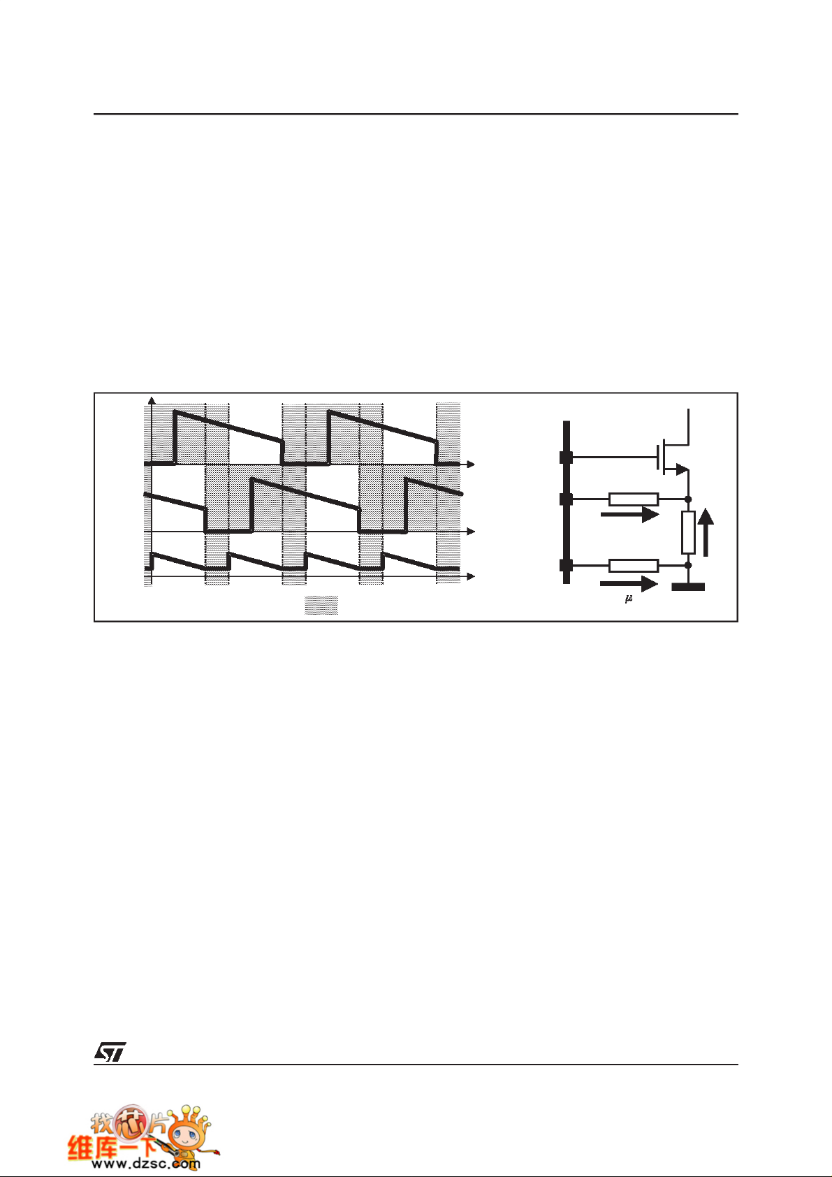
Oscillator
The switching frequency is internally fixed to 300kHz. The internal oscillator generates the triangular waveform
for the PWM charging and discharging with a constant current an internalcapacitor. The current delivered to the
oscillator is typically 25
tween OSC pin and GND or Vcc. Since the OSC pin is maintained at fixed voltage (typ). 1.235V, the frequency
is varied proportionally tothe current sunk (forced) from (into) thepin considering the internal gainof 12KHz/
In particular connecting it to GND the frequency is increased (current is sunk from the pin), while connecting
ROSC to Vcc=12V the frequency is reduced (current is forced into the pin), according to the following relationships:
µA(F
= 300KHz) and maybe varied using an external resistor (R
SW
) connected be-
OSC
µ
A.
R
vs. GND: fS300kHz
OSC
R
OSC
Note that forcing a 25
oscillator.
Figure 1. R
Rosc(KΩ) vs. 12V
vs. Switching Frequency
OSC
7000
6000
5000
4000
3000
2000
1000
0
0 100 200 300
vs. 12V: f
S
300kHz
1.237
----------------------- -------
R
OSC
12 1.237–
------------------------ ------ 12
+
R
OSC
Ω()
K
KΩ()
kHz
-----------⋅+
12
µ
kHz
-----------
⋅
µA
A
300kHz
300kHz
14.82 106⋅
------------------------------+==
R
12.918 107⋅
----------------------- ---------–==
R
OSC
OSC
KΩ()
KΩ()
µA current into this pin, the device stops switching because no current is delivered to the
1000
900
800
700
600
500
400
300
200
Rosc(KΩ) vs. GND
100
0
300 400 500 600 700 800 900 1000
Frequency (KHz)
Frequency(KHz)
8/27
Download from www.ICminer.com Electronic-Library Service

L6917
Digitalto AnalogConverter
The built-in digital to analog converter allows the adjustment of the output voltage from 1.100V to 1.850V with
25mV steps as shown in the previous table 1. The internal reference is trimmed to ensure the precision of 0.8%
and a zero temperature coefficient around 70°C. The internal reference voltage for the regulation is programmed by the voltage identification (VID) pins. These are TTL compatible inputs of an internal DAC that is
realized by means of a series of resistors providing a partition of the internal voltage reference. The VID code
drives a multiplexer that selects a voltage on a precise point of the divider. The DAC output is delivered to an
amplifier obtaining the V
provided (realized with a 5
to leave the pin floating, while to program a logic ”0” it is enough to short the pin to GND.
The voltage identification (VID) pin configuration also sets the power-good thresholds (PGOOD) and the overvoltage protection (OVP) thresholds.
SoftStart and INHIBIT
At start-up a ramp is generated increasing the loop reference from 0V to the final value programmed by VID in
2048 clock periods as shown in figure 2.
Before soft start,the lower power MOS are turned ONafter that V
to discharge the output capacitor and to protect the load from high side mosfet failures. Once soft start begins,
the reference is increased; when it reaches the bottom of the oscillator triangular waveform (1V typ) also the
upper MOS begins to switch and the output voltage starts to increase with closed loop regulation. At the end of
the digital soft start, thePower Good comparator is enabled and the PGOOD signal is then driven high (See fig.
2). The Negative Current Limit comparators and Under Voltage comparator are enabled when the reference
voltage reaches 0.8V.
The Soft-Start will not take place, if both Vcc and VCCDR pins are not above their own turn-on thresholds. During normal operation, if any under-voltage is detected on one of the two supplies the device shuts down.
Forcing the OSC/INH/FAULT pin to a voltage lower than 0.8V the device enter in INHIBIT mode: all the power
mosfets are turned off until this condition is removed. When this pin is freed, the OSC/INH/FAULT pin reaches
the band-gap voltage and the soft start begins.
voltage reference (i.e. the set-point of the error amplifier). Internal pull-ups are
PROG
µA current generator up to 3.3V max); in this way, to program a logic ”1” it is enough
reaches 2V (independently by Vcc value)
CCDR
Figure 2. Soft Start
VIN=V
CCDR
V
LGATEx
V
OUT
PGOOD
Turn ON threshold
2V
t
t
t
2048 ClockCycles
Timing Diagram Acquisition:
t
CH1 = PGOOD; CH2 = V
; CH4 = LGATEx
OUT
9/27
Download from www.ICminer.com Electronic-Library Service

L6917
Driver Section
The integrated high-current drivers allow using different types of power MOS (also multiple MOS to reduce the
RDSON), maintaining fast switching transition.
The drivers for the high-side mosfets use BOOTx pins for supply and PHASEx pins for return. The drivers for
the low-side mosfets use VCCDR pin for supply and PGND pin for return. A minimumvoltage of 4.6V at VCCDR
pin is required to start operations of the device.
The controller embodies a sophisticated anti-shoot-through system to minimize low side body diode conduction
time maintaining good efficiency and saving the use of Schottky diodes. The dead time is reduced to few nanoseconds assuring that high-side and low-side mosfets are never switched on simultaneously: when the highside mosfet turns off, the voltage on its source begins to fall; when the voltage reaches 2V, the low-side mosfet
gate drive isapplied with 30ns delay. When the low-side mosfet turnsoff, the voltage at LGATEx pin is sensed.
When it drops below 1V, the high-side mosfet gate drive is applied with a delay of 30ns.
If thecurrent flowing in the inductor is negative, the source of high-side mosfet will never drop. To allow the turning on of the low-sidemosfet even in this case, a watchdog controller is enabled: after 240ns, the low side mosfet is switched on so allowing the negative current of the inductor to recirculate. This mechanism allows the
system to regulate even if the current is negative.
The BOOTx andVCCDR pins are separated from IC’s power supply (VCC pin) as well as signal ground (SGND
pin) and power ground (PGND pin) in order to maximize the switching noise immunity. The separated supply
for the different drivers gives highflexibility inmosfet choice, allowing the useof logic-level mosfet. Several combination of supply can be chosen to optimize performance and efficiency of the application. Power conversion
is also flexible, 5V or 12V bus can be chosen freely.
Placement of the power mosfets is critical: long and narrow trace length from UGATEx and LGATEx pins to the
mosfets’ gates may cause high amount of ringing due to the resonance between inductance of the trace and
the gate capacitance of the mosfet. A gate resistance of a few ohms can help in reducing ringing and power
dissipation of the controller without compromising system efficiency.
The peak current is shown for both the upper and the lower driver of the two phases in figure 3. A 10nF capacitive load has been used. For the upper drivers, the source current is 1.9A while the sink current is 1.5A with
V
BOOT-VPHASE
VCCDR = 12V.
= 12V; similarly, for the lower drivers,the source current is 2.4A while the sink current is2A with
Figure 3. Drivers peak current: High Side (left) and Low Side (right)
CH3 = HGATE1; CH4 = HGATE2 CH3 = LGATE1; CH4 = LGATE2
10/27
Download from www.ICminer.com Electronic-Library Service
L6917
CurrentReadingand Over Current
The current flowing trough each phase is read using the voltage drop across the low side mosfets r
across a sense resistor (R
) and internally converted into a current. The transconductance ratio is issued
SENSE
by the external resistor Rg placed outside the chipbetweenISENx and PGNDSx pins toward the reading points.
The full differential current reading rejects noise and allows to place sensing element in different locations without affecting the measurement’s accuracy. The current reading circuitry reads the current during the time in
which the low-side mosfet is on (OFF Time). During this time, the reaction keeps the pin ISENx and PGNDSx
at the same voltage while during the time inwhich the reading circuitry is off, an internal clamp keeps these two
pins at the same voltage sinking from the ISENx pin the necessary current.
The proprietary current reading circuit allows a very precise and high bandwidth reading for both positive and
negative current. This circuit reproduces the current flowing through the sensing element using a high speed
Track & Hold transconductance amplifier. In particular, it reads the current during the second half of the OFF
time reducing noise injection into the device due to the mosfet turn-on (See fig. 4).
Figure 4.
I
LS1
LGATEX
I
ISENx
Rg
Rg
SENSE
R
I
LS2
Total current
information
ISENX
PGNDSX
DSON
or
PHASE
I
Track & Hold
50µA
This circuit sources a constant 50µA current from the PGNDSx pin and keeps the pins ISENx and PGNDSx at
the same voltage. Referring to figure 4, the current that flows in the ISENx pin is then given by the following
equation:
R
SENSEIPHASE
----------------------- ---------------- -------+
Where R
I
ISENx
is an external sense resistor or the r
SENSE
50µA
tance resistor used between ISENx and PGNDSx pins toward the reading points; I
⋅
+==
R
g
, on of the low side mosfet and Rg is the transconduc-
dson
50µAI
INFOx
is the current carried
PHASE
by each phase and, in particular, the current measured in the middle of the oscillator period
The current information reproduced internally is represented by the second term of the previous equation as
follow:
R
I
INFOx
SENSEIPHASE
------------------------ ---------------- ------=
R
⋅
g
Since the current is read in differential mode, also negative current information is kept; this allow the device to
check for dangerous returning current between the two phases assuring the complete equalization between the
phase’s currents.
From the current information of each phase, information about the total current delivered (I
and the average current for each phase (I
AVG
=(I
INFO1+IINFO2
)/2 ) is taken. I
INFOX
FB=IINFO1+IINFO2
is then compared to I
AVG
to give the correction to the PWM output in order to equalize the current carried by the two phases.
)
11/27
Download from www.ICminer.com Electronic-Library Service

L6917
Figure 5. HICCUP Mode (left) and OCP threshold and Current information (right)
I
FB
2x35µA=70µA
2x25µA=50µA
Hiccup Mode:
CH1 = FAULT;CH2 = V
; CH3 = IL1;CH4=I
OUT
L2
The over current threshold for each phase is set when I
-50%
I
INFOx
=35µA. Since the over current detection gives
INFOx
25µA
-12.5µA
35µA
100%
140%
I
OUT
I
OUT
origin to Hiccup cycles (and the output voltage goes down to zero, with information losses for the microprocessor) the over current threshold must be greater than the nominal current.
Placing the OC threshold at +40% gives a margin to sustain the heavy load transient issued by the processor.
As a consequence, the transconductance resistor Rg has to be designed in order to have current information of
µ
A at 140% of the nominal load, corresponding to 25µA at nominal load. Considering the feedback current
35
(I
), this will be equal to 50µA at nominal load and 70µA at over current threshold as shown in figure 5.
FB
Since the device is able to read negative current, negative current limitis also provided and it is set when I
INFOx
= -12.5µA , corresponding to -50% ofthe full nominal current.No current is sunk from theFB pin in this condition.
According to the above relationship, the positive limiting current (I
LIM_POS
placed at one half of the total delivered maximum current and the limiting negative current (I
I
LIM_POS
35µARg⋅
----------------------- ---- I
R
SENSE
LIM_NEG
12.5– µARg⋅
----------------------- ------------ Rg
R
SENSE
) for each phase, which has to be
LIM_NEG
I
⋅
LIMRSENSE
----------------------- --------------===
35µA
), results:
When over current is detected, all mosfets are turned OFF, the device waits for 2048 clock cycles and another
soft-start is implemented. Over Current is always active, also during soft-start. After three Over Current event,
the condition is latched and the device stops working; Vcc turn OFF and ON is required to restart device operation.
Over current is set anyway when I
venient values for I
. Since the OPC intervention threshold is fixed, to modify the percentage with respect to
FB
reaches 35µA. The full load value isonly aconvention to work with con-
INFOx
the load value, it can be simply considered that, for example, to have on OCP threshold of 170%, this will correspond to I
=35µA(IFB=70µA). The full load current will then correspond to I
INFOx
= 20.5µA(IFB=41µA).
INFOx
Over current is managed as an under voltage: after a combination of three of then, the device latches the condition and the FAULT pin is driven high.
The full differential path helps the designer to place sensing element where wanted. Transconductance Rg resistors must be placed as close as possible to ISENx and PGNDSx pins in order to reject noise from the device.
Keeping the traces parallel and guarded by a power plane results in common mode coupling for any picked-up
noise.
12/27
Download from www.ICminer.com Electronic-Library Service

L6917
CurrentSharing
Active current sharing is implemented using the information from transconductance differential amplifier in an
average current mode control scheme. A current reference equal to the average of the read current (I
internally built;the errorbetween theread current and thisreference is converted to a voltage with a proper gain
and it is used to adjust the duty cycle whose dominant value is set by the error amplifier at COMP pin.
The current sharing control is a high bandwidth control allowing current sharing even during load transients.
The current sharing error is affected by the choose of external components; choose precise Rg resistor (±1%
is necessary) to sense the current. The current sharing error is internally dominated by the voltage offset of
transconductance differential amplifier; considering a voltage offset equal to 2mV across the sense resistor, the
current reading error is given by the following equation:
∆
∆
Where
I
READ
For Rsense=4m
I
READ
--------------------
I
MAX
is the difference between one phase current and the ideal current (I
Ω and Imax=40A the current sharing error is equal to 2.5%, neglecting errors due to Rg and
2mV
---------------------- ------------------=
R
SENSEIMAX
⋅
MAX
/2).
Rsense mismatches.
Figures 6 and 7 show the current sharing error obtained at 0A and 30A using a sense resistor or the low side
mosfet’s R
as sensing element. The static error obtained using the R
dsON
is due to the tolerance of this
dsON
parameter (up to 30%).
AVG
)is
Figure 6. Current Sharing Error using R
CH1 = PHASE1; CH2 = PHASE2; CH3 = IL2; CH4 = I
as sensing element at 0A (left) and 30A (right).
dsON
L1
13/27
Download from www.ICminer.com Electronic-Library Service

L6917
Figure 7. Current Sharing Error using R
CH1 = PHASE1; CH2 = PHASE2; CH3 = IL2;CH4=I
SENSE
as sensing element at 0A (left) and 30A (right)..
L1
Integrated Droop Function
The device uses a droop function to satisfy the requirements of high performance microprocessors, reducing
the size and the cost of the output capacitor.
This method ”recovers” part of the drop due to the output capacitor ESR in the load transient, introducing a dependence of the output voltage on the load current
As shown in figure 8, the ESR drop is present in any case, but using the droop function the total deviation of the
output voltage is minimized. In practice the droop function introduces a static error (Vdroop in figure 8) proportional to the output current. Since the device has anaverage current mode regulation, the information about the
total current delivered is used to implement the Droop Function. This current (equal to the sum of both I
INFOx
is sourced from the FB pin. Connecting a resistor between this pin and Vout, the total current information flows
only in this resistor because the compensation network between FBand COMP has always a capacitor inseries
(See fig. 9). The voltage regulated is then equal to:
V
OUT=VID-RFB·IFB
Since IFBdepends on the current information about the two phases, the output characteristic vs. load current is
given by:
R
SENSE
V
OUT
VID R
------- ---------- ----- I
⋅⋅–=
FB
Rg
OUT
)
Figure 8. Output transient response without (a) and with (b) the droop function
ESR DROP ESRDROP
VMAX
VNOM
VMIN
(a) (b)
14/27
Download from www.ICminer.com Electronic-Library Service
V
DROOP
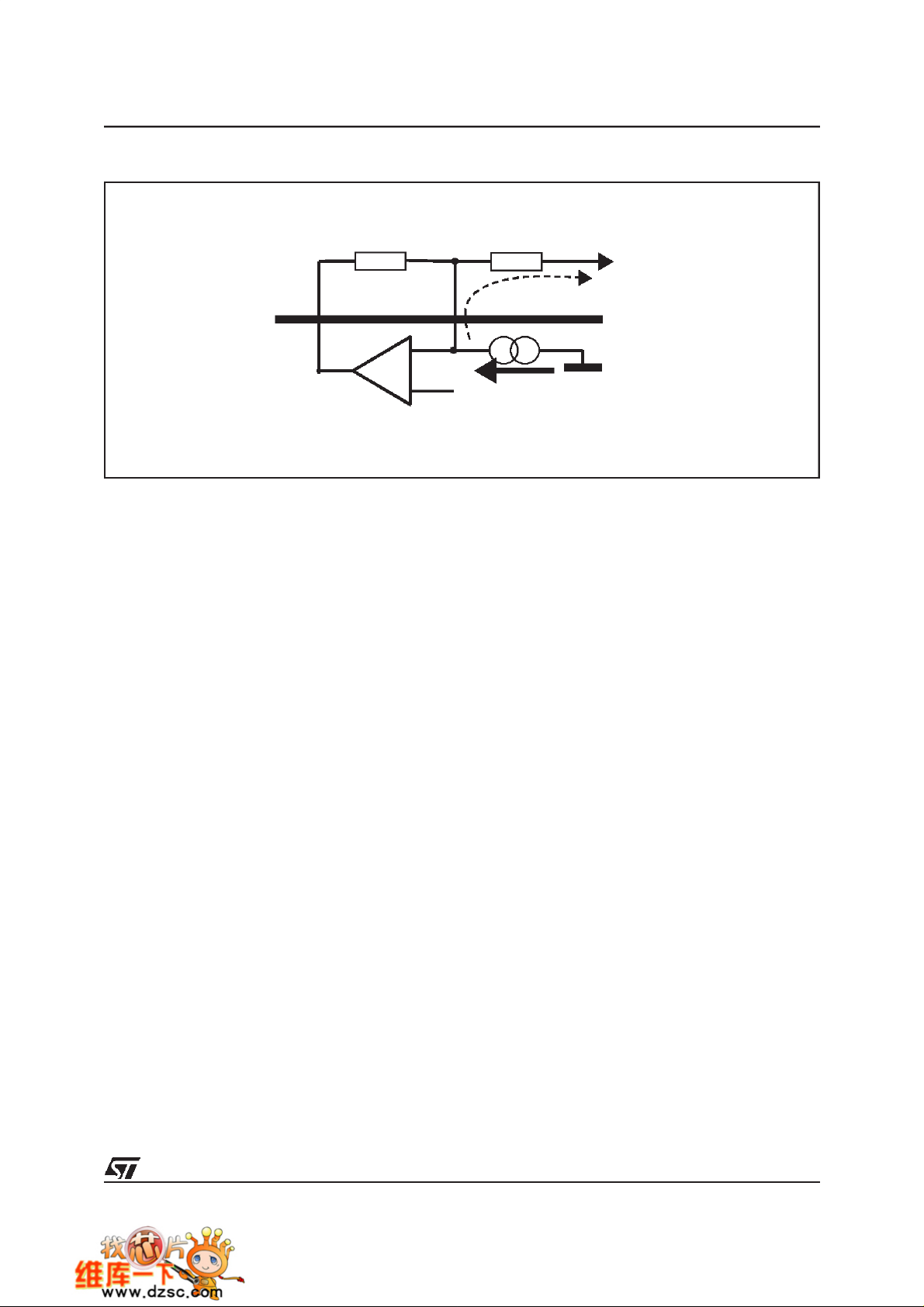
Figure 9. Active Droop Function Circuit
L6917
R
COMP
FB
V
PROG
The feedback current is equal to 50µA at nominal full load (IFB=I
FB
I
FB
INFO1+IINFO2
To VOUT
) and 70µA at the OC threshold,
so the maximum output voltage deviation is equal to:
∆V
FULL_POSITIVE_LOAD
Droop function is provided only for positive load; if negative load is applied, and then I
=+RFB·70µA ∆V
POSITIVE_OC_THRESHOLD
=+RFB·70µA
< 0, no current is
INFOx
sunk from the FB pin. The device regulates at the voltage programmed by the VID.
OutputVoltage Protection and Power Good
The output voltage is monitored by pin VSEN. If it is not within +12/-10% (typ.) of the programmed value, the
powergood output is forced low. Power good is an open drain output and it isenabled only after the soft start is
finished (2048 clock cycles after start-up).
The device provides over voltage protection; when the voltage sensed by the V
pin reaches 2.1V (typ.),the
SEN
controller permanently switches on both the low-side mosfets and switches off both the high-side mosfets in order to protect the CPU. The OSC/INH/FAULT pin is driven high (5V) and power supply (Vcc) turn off and on is
required to restart operations. The over Voltage percentage is set by the ratio between the OVP threshold (set
at 2.1V) and the reference programmed by VID.
OVP[%]
---------------------- ----------------- ----------------- ---------------- ---- - 100
Ref er enc e Voltage VID
2.1V
⋅=
()
Under voltage protection is also provided. If the output voltage drops below the 85% of the reference voltage for
more than one clock period the device turns off all mosfets and waits for 2048 clock cycles before another softstart. An Under Voltage event is then managed as an Over Current event; after a combination of three of them,
the device latches the condition and the FAULT is driven high.
Both Over Voltage and Under Voltage are active also during soft start (Under Voltage after than Vout reaches
0.8V). The reference voltage used to determine the UV thresholds is nowthe increasing voltage driven by the
2048 soft start digital counter.
RemoteVoltage Sense
A remote sense buffer is integrated into the device to allowoutput voltage remotesense implementation without
any additional external components. In this way, the output voltage programmed is regulated between the remote buffer inputs compensating motherboard trace losses or connector losses if the device is used for a VRM
module. The low offset amplifier senses the output voltage remotely through the pins FBR and FBG (FBR is for
the regulated voltage sense while FBG is for the ground sense) and reports this voltage internally at VSEN pin
15/27
Download from www.ICminer.com Electronic-Library Service

L6917
with unity gain eliminating the errors. Keeping the FBR and FBG traces parallel and guarded by a power plane
results in common mode coupling for any picked-up noise.
If remote sense is not required, the output voltage is sensed by the VSEN pin connecting it directly to the output
voltage. In this case the FBG and FBR pins must be connected anyway to the regulated voltage.
Input Capacitor
The input capacitor has to sustain the ripple current produced during the on time of the upper MOSFETS. Considering thedual phase topology, the input rms currentis highly reduced because of the peak current is one half
if compared with a single-phase solution.
Input capacitor must have a low ESR to minimize the losses. The rms value of this ripple is:
I
OUT
------------ D1D–
=
I
rms
Where D is the duty cycle. The equation reaches its maximum value width D=0.5. The losses in worst case are:
2
()⋅⋅
PESRI
Input bulk capacitor must be equally divided between high-side drain mosfets and placed as close as possible
to reduce switching noise above all during load transient. A symmetrical power path will help to improve transient response. Input coil may be used taking from this point the supply for the controller VCC and VCCDRV,
designing a ’star connection’.
IC’s power supplies filter capacitor must be placed as close as possible to VCC and VCCDRV pins; for the VCC
pins a typical value is of 1
tering a series resistor of a few tenth ohm is suggested since the device typically works with the same power
supply used for the power conversion (noisy because of the switching mosfet).
Capacitor on VCCDRV pin filter the low-side drivers power supply toward the PGND pin; 1
ommended.
The 12V input power bus can be used to supply the bootstrap capacitor alone or together with a 5.1V zener
diode in series and a 1
side mosfets with a good compromise of efficiency and controller power dissipation. Alternatively a linear regulator can be used to produce the supply for high-side and low-side power mosfet drivers. This can help to optimize the choose of switching frequency, controller power dissipation and overall efficiency.
µF and must be used connected between VCC and SGND pins. For better noise fil-
µF capacitor for filtering. A gate-source voltage of 7V is so ready to switch on the high-
2
⋅=
rms
µF capacitor is rec-
OutputCapacitor
Since the microprocessors require a current variation beyond 50A doing load transients, with a slope in the
range of tenth A/
Dual phase topology reduces the amount of output capacitance needed because of faster load transient response (switching frequency is doubled at the load connections). Current ripple cancellation due to the 180°
phase shiftbetween the twophases also reduces requirements on the output ESR tosustain a specified voltage
ripple.
When a load transient is applied to the converter’s output, for first few microseconds the current to the load is
supplied by the output capacitors. The controller recognizes immediately the load transient and increases the
duty cycle, but the current slope is limited by the inductor value.
The output voltage has a first drop due to the current variation inside the capacitor (neglecting the effect of the
ESL):
µs, the output capacitor is a basic component for the fast response of the power supply.
∆V
A minimum capacitor value is required to sustain the current during the load transient without discharge it. The
16/27
OUT
= ∆I
OUT
· ESR
Download from www.ICminer.com Electronic-Library Service
L6917
voltage drop due to the output capacitor discharge is given by the following equation:
2
Where D
∆
V
OUT
is the maximum duty cycle value. The lower is the ESR, the lower is the output drop during load
MAX
----------------------- ----------------- ----------------- ---------------- ---------------- ---=
2C
OUTVINMINDMAXVOUT
∆
I
OUT
⋅
L
–⋅()⋅⋅
transient and the lower is the output voltage static ripple.
Inductor design
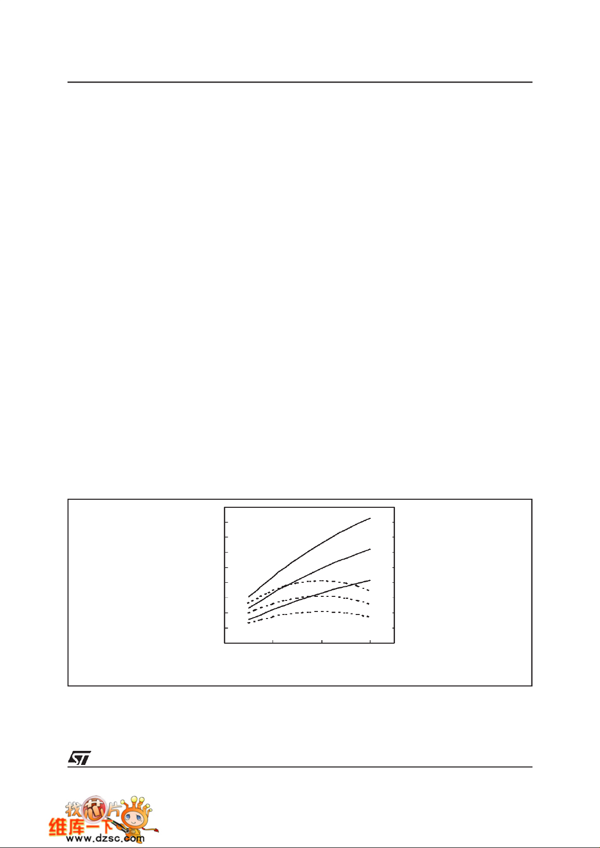
The inductance value is defined by a compromise between the transient response time, the efficiency, the cost
and the size. The inductor has to be calculated to sustain the output and the input voltage variation to maintain
∆
the ripple current
IL between 20% and 30% of the maximumoutput current. The inductance value can be cal-
culated with this relationship:
V
Where f
L
is the switching frequency, VINis the input voltage and V
S
fs IL∆⋅
–
INVOUT
----------------------- -------
=
V
-------------- -
⋅
V
OUT
IN
is the output voltage.
OUT
Increasing the value of the inductance reduces the ripple current but, at the same time, reduces the converter
response time to a load transient. The response time is the time required by the inductor to change its current
from initial to final value. Since the inductor has not finished its charging time, the output current is supplied by
the output capacitors. Minimizing the response time can minimize the output capacitance required.
The response time to a load transient is different for the application or the removal of the load: if during the application ofthe loadthe inductor is charged by a voltage equal tothe difference between the input and the output
voltage, during the removal it is discharged only by the output voltage. The following expressions give approximate response time for DI load transient in case of enough fast compensation network response:
t
application
LI
---------------------- --------=
–
VINV
∆⋅
OUT
t
removal
∆⋅
LI
---------------=
V
OUT
The worst condition depends on the input voltage available and the output voltage selected. Anyway the worst
case is the response time after removal of the load with the minimum output voltage programmed and the maximum input voltage available.
Figure 10. Inductor ripple current vs V
9
out
L=1.5µH, Vin=12V
8
L=2µH,
Vin=12V
L=3µH,
Vin=12V
L=1.5µH,
Vin=5V
L=2µH,
Vin=5V
InductorRipple [A]
7
6
5
4
3
2
1
L=3µH, Vin=5V
0
0.5 1.5 2.5 3.5
OutputVoltage[V]
17/27
Download from www.ICminer.com Electronic-Library Service
L6917
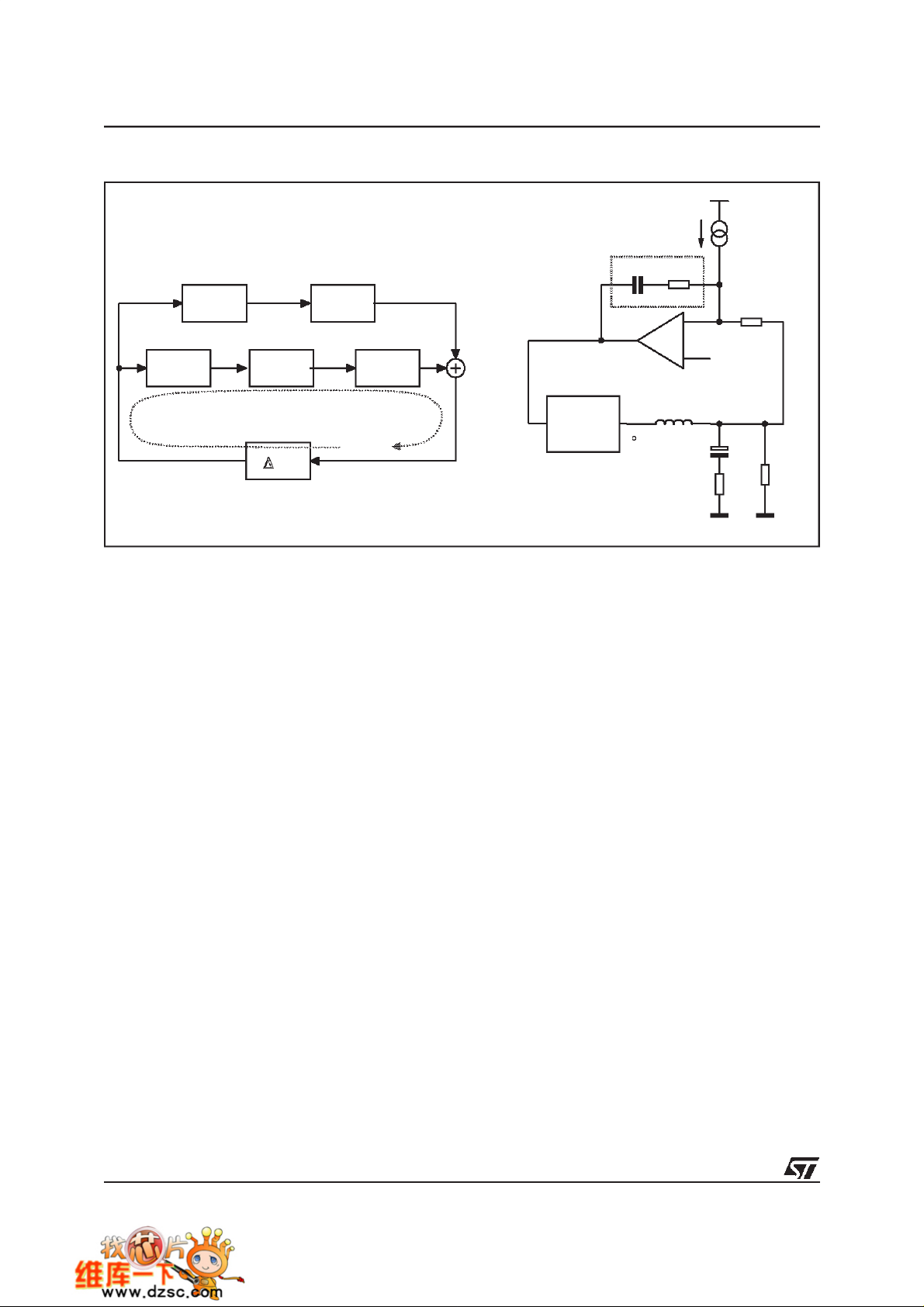
Figure 11. Control Loop Scheme
IFB
RFCF
R
FB
REF
L
IN
Cout
ESR
VOUT
Rout
Av -ZF/RFB
Ac Rs/Rg -ZF
d
VOUT
1/∆V
osc
IFBIOUT
GLOOPI
VCOMP
VCOMP
PWM
Z
F
d•V
AverageCurrent Mode Compensation NetworkDesign
The average current mode control loop is reported in figure 11. The current information IFBsourced by the FB
pin flows into R
implementing the dependence of the output voltage from the read current.
FB
Two different loops are present and precisely a current loop internal to a voltage loop.The current gain (Ac)and
voltage gain (Av) present in the above figure are defined by the following relationships:
()
Av s
Ac s()
V
OUT
-------------- -
d
I
OUT
------------
===
d
{}
....
....{}
V
IN
V
IN
-------------- -
R
OUT
------------------------ ----------------- ----------------- ----------------- --------------- ----------------- ----------------- -⋅===
S2C
OUT
L
---⋅
sESRC
2
1s+ ESR C
----------------------- ----------------- ---------------- ----------------- ---------------- ---------------- ----------------- ---
1s+ESR C
⋅
S2C
⋅
L
---
+
⋅ sESRC
OUT
⋅
2
⋅
⋅⋅
OUT
⋅⋅
OUT
OUT
OUT
L
-----------------------+⋅
2R
⋅
L
-----------------------+
2R
⋅
+⋅+⋅
OUT
1
+
1
OUT
The current loop gain may now be expressed by the following equation:
Rs
--------
Rg
Z
F
----------------- -⋅⋅⋅–==
Vosc
∆
s()
Where
G
LOOPI
Ac s()Rs Z
s
-----------------------------------------------
()
Rg Vosc
∆⋅
s
()⋅⋅
F
-------------- -
R
∆Vosc has a typical value of 2V and Z
V
IN
------------------------------------------------------------------------------------------------------------------------------
2
OUT
C
S
OUT
(s) is the impedance of the series RF-CF. The current loop gain
F
1s+ ESR C
L
---⋅ s ESR C
2
⋅⋅
OUT
OUT
L
---------------------- -+⋅
⋅
2R
1+⋅+⋅
OUT
is designed to obtain a high DC gain to minimize static error and cross the 0dB axes with a constant -20dB/dec
ω
slope with a crossover frequency
poles. Both the poles are fixed once the output filter is designed and alsothe zero (
by the maximum current deliverable by the converter. To obtain the desired shape an R
considered for the Z
(s) implementation. A zero at ωF=1/RFCFis then introduced together with an integrator.
F
. Neglecting the effect of ZF(s), the transfer function has one zero and two
TI
ω
OUT
=1/R
OUTCOUT
series network is
F-CF
) is fixed
This integrator minimizes the static error while placing the zero in correspondence with the L-C resonance a
simple -20dB/dec shape of the gain is assured (See Figure 12).
18/27
Download from www.ICminer.com Electronic-Library Service

Figure 12. Current loop Gain (left) and Voltage loop Gain (right)
L6917
dB
Ac
G
LOOPI
Z
F
ω
TI
ω
OUT
ω
LC
ω
F
ω
dB
⋅
RgRo
⋅
RRs
FB
ω
TV
ω
OUT
ω
ω
ESR
TI
ω
The RFCFnetwork may be designed considering the desired crossover frequencyωTIas follow:
■ Assuming thatω
■
Given the cross-over frequencyωTI, it results:
== =
R
F
■ Since ω
F=ωLC
F=ωLC
Rg
Ro Vosc∆⋅
------- -
--------------------- ----------
⋅⋅
Rs
:
Since the device works in current mode and then the control loop acts to control the current, the highest is
, and that ZF=RFif ω>ωF, it can be observed that:
VINRFR
⋅⋅
--------------------- ----------------- -----
⋅⋅
Ro Vosc∆Rg
LC
⋅⋅
L
---⋅
2
R
F
----------------------- --------------
------------------------ ------------ -
Ro C
Ro Vosc∆⋅
---------------------- ---------
⋅⋅
Vin
C
OUT
----------------------- ----=
F
Vin
G
LOOPI
ωoωTI⋅
------------------- -
2
ω
LC
ω=ω
()
LC
Rg
--------
Rs
C
ω
S
LC
----------
⋅=
ω
O
OUTωTI
2
⋅
OUT
Rg
Vosc∆
------- -
------------------
⋅⋅
Rs
Vin
L
----------------
2 ωTI⋅
ω
TI
the fastest is the device to react after a loadtransient. The placement of this singularity must consider the worst
case for the load and precisely the maximum output current (minimum output resistance R
OUT
).
The voltage loop gain may be expressed by the following relationship:
1
------- ---------- -
Vosc∆
----------------------- --------
⋅⋅
+
1G
LOOPI
R
OUT
---------------------- ------
⋅⋅==
Rs RFB⋅
⋅
Rg
ZFs()
-------------- -
R
FB
1
-------------------
s
---------+
1
ω
TI
Assuming that G
V
OUT
-------------------
G
LOOPV
I>>1 and after substitution and simplification the final expression for GLOOPV is given by:
LOOP
==
s()
V
COMP
V
COMP
-------------------
⋅ Av s()
V
OUT
1 s ESR C
G
LOOPV
s() ...{}
----------------------- ----------------- ------------
1sR
Where the additional pole placed at the current loop
is not always G
>>1. The LC resonance disappears thanks to the average current mode control and the
LOOPI
–
⋅⋅+
⋅⋅+
OUTCOUT
ω
TI
OUT
must be inserted to consider that the current loop gain
system is automatically stable if ESR issmall enough.
Since all the above modeling are valid at frequencies much lower than the switching frequency, the highest is
this, the highest may be the converter’s loop bandwidth (both current and voltage). In this way the converter is
able to fast react after a load transient following, with the current delivered by the inductors, the currentrequired
by the load minimizing the number of the output capacitor required.
The average current mode compensation network is then designed as follow:
,
19/27
Download from www.ICminer.com Electronic-Library Service

L6917
■
Given the voltage loop bandwidth
Rs RFB⋅
== =
ω
TI
■ Once the current loop bandwidth is defined, the R
-----------------------
ω
⋅⋅ω
TV
Ro Rg⋅
ω
, the current loop bandwidth wTI is extracted from the following:
TV
ω
ESR
-------------- -
ω
O
Rs RFB⋅
-----------------------
⋅⋅ ω
TV
Ro R g⋅
FCF
Ro C
⋅
⋅
OUT
OUT
TV
---------------------- ---------- -
ESR C
network may be designed as shown previously.
Rs RFB⋅
----------------------- --
⋅
ESR R g⋅
DemoBoard Description
The L6917 demo board shows the operation of the device in a dual phase application. This evaluation board
allows voltage adjustability (1.100V - 1.850V) through the switches S0-S4 and high output current capability.
The 12V input rail supplies both the device and the high-side drain for the power conversion.
2
The board has been layed out with the possibility to use up to two D
PACK mosfets for the low side switch in
order to give maximum flexibility in the mosfet’s choice.
The four layers demo board’s copper thickness is of 70
µm in order to minimize conduction losses considering
the high current that the circuit is able to deliver.
Figure 13 shows the demo board’s schematic circuit.
Figure 13. Demo Board Schematic
Vin
GNDin
DZ1
JP1
L1
D1
Q1a Q3a
S4
S3
S2
S1
S0
JP2
R16
D4C6
Q2C4
Q1
R2
VCCDR
BOOT1
UGATE1
PHASE1
LGATE1
ISEN1
PGNDS1
OSC / INH
SGND
VID4
VID3
VID2
VID0VID1
2
5
4
3
1
13
U1
14
L6917
22
21
20
19
18
17
7
11 12
FBR FBG
C8
R15
R18
R13
R6
R5
6
24
25
26
27
16
15
28
23
10
9
8
VCC
BOOT2
UGATE2
PHASE2
LGATE2
ISEN2
PGNDS2
PGND
PGOOD
VSEN
FB
COMP
R14
R17
R12
R10
C7
D3
Q4 C3
Q3
R3
R4
R7
R8
C2
C5
L2
D2
R1
JP3
C1
R9
C9,C10
C14,
C24
C11..C13
R19
R20
VoutCORE
GNDCORE
PGOOD
JP5JP4
FBG
FBR
20/27
Download from www.ICminer.com Electronic-Library Service
L6917
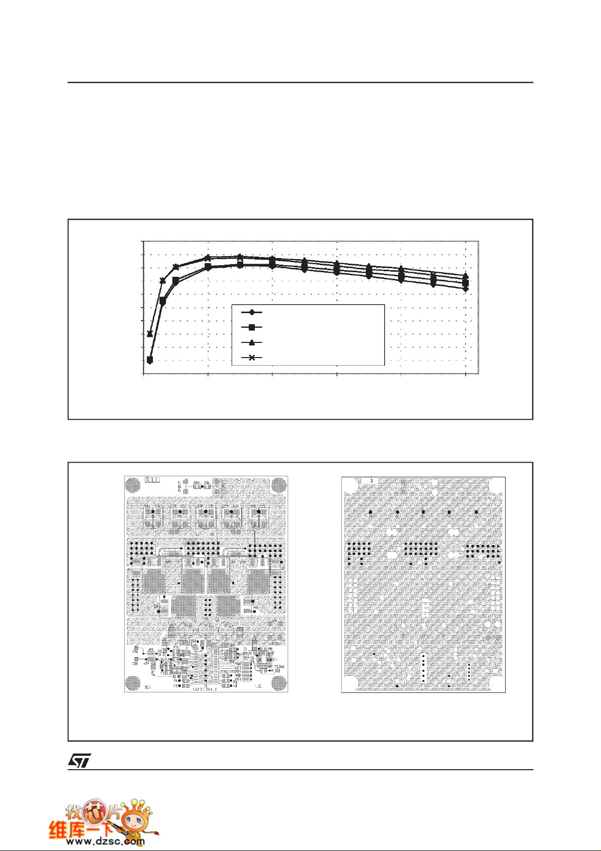
Efficiency
Figure 14 shows the demo board measured efficiency versus load current for different values of input voltage
and mosfet configurations.
Measures were done at Vin=5V and Vin=12V with low side mosfet composed by a single STB90NF03L (30V,
Ω
5.6m
When 5V input is considered, the 12V bus supplies the IC and the mosfet’ drivers.
Figure 14. Efficiency
typ @ Vgs=10V) or a couple of STB70NF03L (30V, 8mΩtyp @ Vgs=10V) to reduce equivalent R
95
90
85
80
75
70
65
Efficiency [%]
60
55
50
45
0 1020304050
Vin = 12V; LS=STB90NF03L
Vin = 12V; LS=2xSTB70NF03L
Vin = 5V; LS=2xSTB70NF03L
Vin = 5V; LS=STB90NF03L
OutputCurrent [A]
dsON
.
PCB and Components Layouts
Figure 15. PCB and Components Layouts
Component Side Internal PGND Plane
21/27
Download from www.ICminer.com Electronic-Library Service

L6917
Figure 16. PCB and Components Layouts
Internal SGND Plane Solder Side
DesignExample.
■
Output Voltage (nominal) 1.700V
■
Output Current (nominal) 45A
■
Static tolerance +100mV; -50mV
Considering the high slope for the load transient, a high switching frequency has to be used. In addition to fast
reaction, this helps in reducing output and input capacitor. Inductance value is also reduced.
A switching frequency of 300kHz for each phase is then considered allowing large bandwidth for the compensation network.
■ Current Reading Network and Over Current:
Since the maximum output current is 45A, the over current threshold has to be set at 140% of the
maximum nominal current, the over-current threshold has thento be setat 31.5A. Considering tosense
the output current across the low-side mosfet RdsON, STB90NF03L has 6.5mΩ max at25°that
becomes 9.1mΩ considering the temperature variation (+40%); the resulting transconductance resistor
Rg has to be:
I
■
Droop function Design:
Rg
RdsON⋅
MAX
----------------------- --------------- -
35
µ
⋅
31.5 9.1m
----------------------- -------
µ
35
8.2k
Ω===
(R3 to R6)
Considering a voltage drop of 100mV at full load, the feedback resistor RFB has to be
==
R
FB
voltage drop at OCP threshold results in 140mV.
22/27
100mV
-------------------
50µA
(R7)
2kΩ
Download from www.ICminer.com Electronic-Library Service

■
Inductor design:
Each phase has to deliver up to 22.5A; considering a current ripple of 5A (<25%), the resulting
inductance value is:
L6917
■
Output Capacitor:
L
Vin Vout–
----------------------- ------
I∆
d
-----------⋅
Fsw
12 1.7–
---------------------
5
1.7
--------
12
1
--------------------⋅⋅ 1µH== =
300000
(L1, L2)
Six PANASONIC SP-CAP EEFUE0D27 (270µF, 15mΩmax) has been used implementing a resulting
ESR of 2.5mΩresulting in a voltage drop of 45A*2.5mΩ=112.5mV after a load transient.
■ Compensation Network:
A voltage loop bandwidth of 40kHz is considered to let the device fast react after load transient.
⋅
The R
FCF
■
VID settings:
fTV= 20kHz=>
network results:
Rg
------- -
R
F
Rs
Rs R
f
TIfTV
∆
Vosc
------------------
⋅⋅⋅
Vin
C
----------------------- ----
F
---------------------- ---
⋅ 20k
ESR Rg⋅
L
-- -
ω
2
-----------------------
2C
⋅
R
-------------
TI
7.8m
L
OUT
F
FB
8.2k
--- -- -
⋅⋅⋅⋅
12
------------------------
2 1.62m⋅
------------------------ ----- 3.4nF== =
8.2k
⋅ 15.2kHz== =
µ
2
1
------ - 2
2
1 µ
⋅
7.8m 2k
----------------------- -------
2.5m 8.2k⋅
π
15.2k
(C2)
Ω== =
8.2k
(R8)
Considering the 100mV voltage drop programmed by thefeedback resistor and the static tolerance, the
VID are set for 1.775V (00011 code) in order to have a ±25mV of margin in the regulation.
Part List
R1 10k SMD 0805
R2, R9, R20 Not Mounted SMD 0805
R3, R4, R5, R6 8.2k 1% SMD 0805
R7 2k 1% SMD 0805
R8 10k SMD 0805
R10 82Ω SMD 0805
R12 to R15 0
C2 4.7n SMD 0805
C3, C4 100n SMD 0805
C5, C6, C7 1µ Ceramic SMD 1206
C8, C9, C10 10
C11, C12, C13 100µ / 20V OSCON 20SA100M Radial 10x10.5
C19 to C24 270µ/ 2V PANASONIC SP-CAP SMD 7343
L1, L2 1µ 77121 Core – 7 Turns or
U1 L6917 STMicroelectronics SO28
Q1, Q3 STB90NF03L STMicroelectronics
Q2, Q4 STB70NF03L STMicroelectronics
D1, D2 STPS340U STMicroelectronics SMB
D3, D4 1N4148 STMicroelectronics SOT23
Ω
µ
Ceramic SMD 1206
TO50-52B Core – 6 Turns
SMD 0805
2
D
PACK
2
D
PACK
23/27
Download from www.ICminer.com Electronic-Library Service

L6917
Application Idea: 12V input 3.3V / 5V 40A output
Figure 17 shows the device in a high current server power supply application.
Adding an external resistor divider after the remote sense buffer gives the possibility to increase the regulated
voltage. Considering for example a divider by two (two equal resistors)the DAC range is doubled from 2.200V
to 3.700V with 50mV binary steps. It is then possible to regulate the 3.3V and 2.5V rails from the 12V available
from the AC/DC converter. The 5V railcan be obtained modifying the external divider. The regulator assures all
the advantages of the dual phase conversion (especially in the 5V conversion where the duty cycle is near the
50% and practically no ripple is present in the input capacitors) and a 300kHz free-running frequency that reduces components size. Output current ranges from 35A up to 50A.
Figure 17. Server power supply schematic
Vin
GNDin
R16
D4C6
Q2C4
L1
Q1
D1
S4
S3
S2
S1
S0
R2
VCCD R
D5
BOOT 1
UGATE1
P HASE1
LGATE1
ISEN1
PGND S1
OSC / INH
VID4
VID2VID3
VID1
VID0
2
5
4
3
1
13
U1
14
L6917
22
21
20
19
18
17
7
11 12
FB R FBG
C8
R15
R18
R13
R6
R5
6
24
25
26
27
16
15
28
23
10
9
8
VCC
BOOT 2
UGA TE2
P HASE2
LGATE2
ISEN 2
P GNDS2
P GND
P GOOD
VSEN
FB
COMPSG ND
R10
C7
D3
Q4 C3
R14
R17
Q3
R12
D6
R3
R4
R7
R8
C2
C5
L2
D2
C1
R9
C9,C10
C11..C13
R19
C14,
C24
R20
R1
VoutCORE
GNDCORE
PGOOD
FBG
FBR
Part List
R1 10k SMD 0805
R3, R4, R5, R6 8.2k 1% SMD 0805
R7 820 1% SMD 0805
R8 10k SMD 0805
R10
R12 to R16 0Ω SMD 0805
R17, R18 0
R19, R20 330Ω SMD 0805
C2 4.7n SMD 0805
C3, C4 100n SMD 0805
C5, C6, C7 1µ Ceramic SMD 1206
C8 10µ Ceramic SMD 1206
C9 to C13
24/27
82
Ω
47µ
Ω
SMD 0805
SMD 0805
Ceramic SMD 1026
Download from www.ICminer.com Electronic-Library Service

Part List
C14, C15 1500µ / 6.3V Radial
L1, L2 4
µ
77121 Core – 10T (30A Out) or
77848 Core – 11T (45A Out)
U1 L6917 STMicroelectronics SO28
Q1, Q3 STB90NF03L STMicroelectronics
Q2, Q4 STB70NF03L STMicroelectronics
D
D
2
PACK
2
PACK
D1, D2 STPS340U STMicroelectronics SMB
D3, D4 1N4148 STMicroelectronics SOT23
Figure 18.
vout
1.700
1.698
1.696
1.694
1.692
1.690
OutputVoltage[V]
1.688
1.686
1.684
-40 -20 0 20 40 60 80 100 120 140
Temperature [C]
L6917
Output Voltage vs. Temperature
49
48
47
46
45
44
IPGNDS [A]
43
42
41
-40 -20 0 20 40 60 80 100 120 140
Temperature [C]
PGNDS Bias Current vs. Temperature
25/27
Download from www.ICminer.com Electronic-Library Service

L6917
DIM.
MIN. TYP. MAX. MIN. TYP. MAX.
A 2.65 0.104
a1 0.1 0.3 0.004 0.012
b 0.35 0.49 0.014 0.019
b1 0.23 0.32 0.009 0.013
C 0.5 0.020
c1 45° (typ.)
D 17.7 18.1 0.697 0.713
E 10 10.65 0.394 0.419
e 1.27 0.050
e3 16.51 0.65
F 7.4 7.6 0.291 0.299
L 0.4 1.27 0.016 0.050
S8°(max.)
mm inch
OUTLINE AND
MECHANICALDATA
SO28
26/27
Download from www.ICminer.com Electronic-Library Service

L6917
Information furnished is believed to be accurate and reliable. However, STMicroelectronics assumes no responsibility for the consequences
of useof such information nor forany infringementof patents orotherrights ofthird partieswhichmayresult from its use.No license isgranted
by implication or otherwise under any patent or patent rights of STMicroelectronics. Specifications mentioned in this publication are subject
to change without notice. This publication supersedes and replaces all information previously supplied. STMicroelectronics products are not
authorized for use as critical components in life support devices or systems without express written approval of STMicroelectronics.
The ST logo is a registered trademark of STMicroelectronics
2001 STMicroelectronics - All Rights Reserved
Australia - Brazil - Canada - China - Finland - France - Germany - Hong Kong - India - Israel - Italy - Japan -Malaysia - Malta - Morocco -
Singapore - Spain - Sweden - Switzerland - United Kingdom - United States.
STMicroelectronics GROUP OF COMPANIES
http://www.st.com
27/27
Download from www.ICminer.com Electronic-Library Service
 Loading...