

查询L6911C供应商
5 BIT PROGRAMMABLE STEP DOWN CONTROLLER
■
OPERATING SUPPL Y IC VOLTAGE FROM 5V
TO 12V BUSES
■
UP TO 1.3A GATE CURRENT CAPABILITY
■
TTL-COMP A T I BLE 5 BIT P ROGR AMMABLE
OUTPUT CO MPLIANT WITH VRM 8.4 :
1.3V TO 2.05V WITH 0.05V BINARY STEPS
2.1V TO 3.5V WITH 0.1V BINARY STEPS
■
VOLTAGE MODE PWM CONTROL
■
EXCELLENT OUTPUT ACCURACY: ±1%
OVER LINE AND TEMPERATURE
VARIATIONS
■
VERY FAST LOAD TRANSIENT RESPONSE:
FROM 0% TO 100% DUTY CYCLE
■
POWER GOOD OU T PUT VO LTA GE
■
OVERVOLTAGE PROTECTION AND
MONITOR
■
OVERCURRENT PROTECTION REALIZED
USING THE UPPER MOSFET'S R
■
200KHz INTERNAL OSCILLATOR
■
OSCILLATOR EXTERNALLY ADJUST ABLE
FROM 50KHz TO 1MHz
■
SOFT START AND INHIBIT FUNCTIONS
APPLICATIONS
■
POWER SUPPLY FOR ADVANCED
MICROPROCESSOR CORE
■
DISTRIBUTED PO WE R SUPP LY
■
HIGH POWER DC-DC REGULATORS
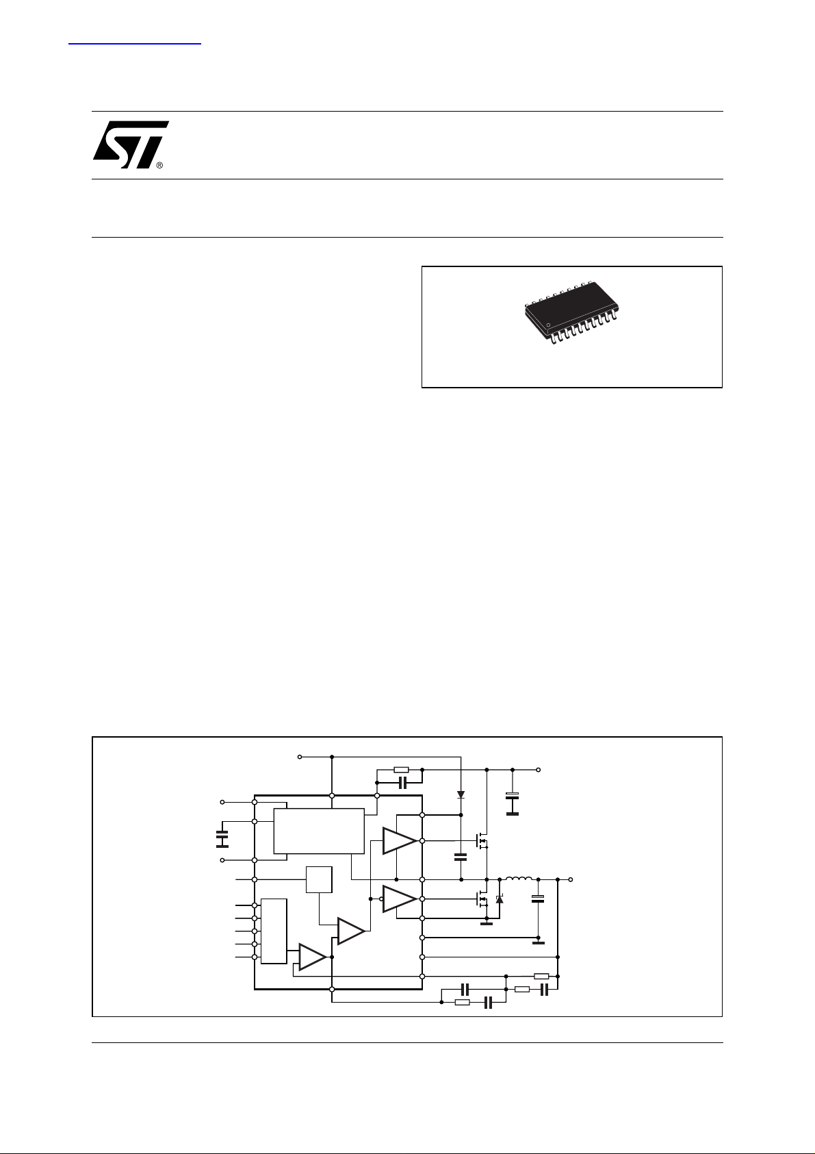
L6911C
WITH SYNCHRONOUS RECTIFICATION
SO-20
dsON
ORDERING NUMB ERS : L6911C
DESCRIPTION
The device is a power supply controller specifically designed to provide a high performance DC/DC conversion for high current microprocessors. A precise 5-bit
digital to analog converter (DAC) allows adjusting the
output voltage from 1.30V to 2.05V with 50mV binary
steps and from 2.1 0V to 3.50V with 100 mV binary steps.
The high precision internal r eference ass ures the selected output voltage to be within ±1%. The high peak
current gate drive affords to have fast switching to the
external power mos providing low switching losses.
The device assures a fast protection against load
overcurrent and load overvoltage. An ex ternal SCR is
triggered to crowbar the input supply in case of hard
over-voltage. An internal crowbar is also provided
turning on the low side mosfet as long as the overvoltage is detected. In case of ove r-current detection,
the soft start capacitor is discharged and the system
works in HICCUP mode.
L6911CTR
(Tape and Reel)
BLOCK DIAGRAM
November 2001
PGOOD
OVP
VD0
VD1
VD2
VD3
VD4
D01IN1260
Vcc 5 to 12V
VCC OCSET
SS
RT
D/A
MONITOR and
PROTECTION
OSC
+
E/A
COMP
+
PWM
BOOT
UGATE
PHASE
LGATE
PGND
GND
VSEN
VFB
Vin 5V to12V
1.300V to 3.500V
Vo
1/20
L6911C
ABSOLUTE MAXIMUM RATINGS
Symbol Parameter Value Unit
V
CC
V
BOOT-VPHASE
V
HGATE-VPHASE
VCC to GND, PGND 15 V
Boot Voltage 15 V
15 V
OCSET, LGATE, PHASE -0.3 to Vcc+0.3 V
RT, SS, FB, PGOOD, VSEN, VID0-4 7 V
OVP, COMP 6.5 V
THERMAL DATA
Symbol Parameter Value Unit
R
th j-amb
T
PIN CONNECTION
Thermal Resistance Junction to Ambient 110 °
T
Maximum junction temperature 150 °
j
Storage temperature range -40 to 150 °
stg
T
Junction temperature range 0 to 125 °
J
(Top view)
C/W
C
C
C
2/20
VSEN
OCSET
SS/INH
VID0
VID1
VID2
VID3
VID4
COMP PGOOD
FB GND
2
3
4
5
6
7
8
9
10
D98IN958
20
19
18
17
16
15
14
13
12
11
RT1
OVP
VCC
LGATE
PGND
BOOT
UGATE
PHASE

PIN FUNCTION
g
g
g
g
g
g
Pin
Num.
1 VSEN Connected to the output voltage is able to manage over-voltage conditions and the PGOOD
2 OCSET A resistor connected from this pin and the upper Mos Drain sets the current limit protection.
Name Description
signal.
The internal 200µA current
The Over-Current threshold is due to the followin
enerator sinks a current from the drain through the external resistor.
equation:
I
I
--------------------------------------------- -=
P
⋅
OCSETROCSET
R
DSon
L6911C
3 SS/INH
The soft start time is pro
internal current
enerator forces through the capacitor 10µA.
This pin can be used to disable the device forcin
rammed connecting an external capacitor from this pin and GND. The
a voltage lower than 0.4V
4 - 8 VID0 - 4 Voltage Identification Code pins. These input are internally pulled-up and TTL compatible. They
are used to program the output voltage as specified in Table 1 and to set the overvoltage and
power good thresholds.
Connect to GND to program a ‘0’ while leave floating to program a ‘1’.
9 COMP This pin is connected to the error amplifier output and is used to compensate the voltage control
feedback loop.
10 FB This pin is connected to the error amplifier inverting input and is used to compensate the voltage
control feedback loop.
11 GND All the internal references are referred to this pin. Connect it to the PCB signal ground.
12 PGOOD This pin is an open collector output and is pulled low if the output voltage is not within the above
specified thresholds.
If not used may be left floating.
13 PHASE This pin is connected to the source of the upper mosfet and provides the return path for the high
side driver. This pin monitors the drop across the upper mosfet for the current limit
14 UGATE High side gate driver output.
15 BOOT Bootstrap capacitor pin. Through this pin is supplied the high side driver and the upper mosfet.
Connect through a capacitor to the PHASE pin and through a diode to Vcc (cathode vs. boot).
16 PGND Power ground pin. This pin has to be connected closely to the low side mosfet source in order to
reduce the noise injection into the device
17 LGATE This pin is the lower mosfet gate driver output
18 VCC Device supply voltage. The operative nominal supply voltage ranges from 5 to 12V.
DO NOT CONNECT V
TO A VOLTAGE GREATER THAN VCC.
IN
19 OVP Over voltage protection. If the output voltage reaches the 17% above the programmed voltage
this pin is driven high and can be used to drive an external SCR that crowbar the supply voltage.
If not used, it may be left floating.
20 RT Oscillator switching frequency pin. Connecting an external resistor from this pin to GND, the
external frequency is increased according to the equation:
f
S
200kHz
4.94 10
-------------------------+=
R
⋅
kΩ()
T
6
Connecting a resistor from this pin to Vcc (12V), the switching frequency is reduced according to
the equation:
f
S
200kHz
4.306 10
---------------------------- -–=
R
⋅
kΩ()
T
7
If the pin is not connected, the switching frequency is 200KHz.
The volta
e at this pin is fixed at 1.23V (typ). Forcing a 50µA current into this pin, the built in
oscillator stops to switch.
3/20
L6911C
ELECTRICAL CHARACTERISTCS
(VCC = 12V, T
= 25°C unless otherwise specified)
amb
Symbol Parameter Test Condition Min. Typ. Max. Unit
V
SUPPLY CURRENT
CC
Icc Vcc Supply current UGATE and LGATE open 5 mA
POWER-ON
Turn-On Vcc threshold VOCSET=4.5V 4.6 V
Turn-Off Vcc threshold VOCSET=4.5V 3.6 V
Rising V
I
Soft start Current 10 µ
SS
threshold 1.24 V
OCSET
OSCILLATOR
Free running frequency R
Total Variation
∆
Ramp amplitude RT = OPEN 1.9 Vp-p
V
osc
= OPEN 180 200 220 KHz
T
6 KΩ < RT to GND < 200 K
Ω -15 15 %
REFERENCE AND DAC
DACOUT Voltage
Accuracy
VID0, VID1, VID2, VID3, VID4
see Table1; Tamb = 0 to 70°C
-1 1 %
VID Pull-Up voltage 4 V
ERROR AMPLIFIER
DC Gain 88 dB
GBWP Gain-Bandwidth Produ ct 10 MHz
SR Slew-Rate COMP=10pF 10
GATE DRIVERS
I
UGATE
R
UGATE
I
LGATE
High Side Source
Current
High Side Sink
Resistance
Low Side Source
- V
V
BOOT
V
V
I
- V
UGATE
BOOT-VPHASE
= 300mA
UGATE
Vcc=12V, V
PHASE
PHASE
LGATE
=12V,
= 6V
=12V,
= 6V
1 1.3 A
24Ω
0.9 1.1 A
Current
R
LGATE
Low Side Sink
Vcc=12V, I
LGATE
= 300mA
1.5 3 Ω
Resistance
Output Driver Dead Time PHASE connected to GND 120 ns
PROTECTIONS
V
Rising 117 120 %
SEN
= 4.5V 170 200 230 µ
OCSET
> OVP Trip, V
SEN
=0V 60 mA
OVP
I
OCSET
I
OVP
Over Voltage Trip
/DACOUT)
(V
SEN
OCSET Current Source V
OVP Sourcing Current V
POWER GOOD
V
Rising 110 112 114 %
SEN
V
Falling 86 88 90 %
SEN
Upper and Lower threshold 2 %
= -5mA 0.5 V
PGOOD
V
PGOOD
Upper Threshold
/DACOUT)
(V
SEN
Lower Threshold
(V
/DACOUT)
SEN
Hysteresis
(V
/DACOUT)
SEN
PGOOD Voltage Low I
A
V/µS
A
4/20

Table 1. VID Settings
VID4 VID3 VID2 VID1 VID0
01111
01110
01101
01100
01011
01010
01001
01000
00111
00110
00101
00100
00011
00010
00001
00000
Output
Voltage (V)
1.30
1.35
1.40
1.45
1.50
1.55
1.60
1.65
1.70
1.75
1.80
1.85
1.90
1.95
2.00
2.05
L6911C
VID4 VID3 VID2 VID1 VID0
11111Output Off
11110 2.1
11101 2.2
11100 2.3
11011 2.4
11010 2.5
11001 2.6
11000 2.7
10111 2.8
10110 2.9
10101 3.0
10100 3.1
10011 3.2
10010 3.3
10001 3.4
10000 3.5
Output
Voltage (V)
Device Description
The device is an i ntegrated circuit r ealized in BCD technol ogy. It provides c omplete control logic and protections
for a high performance step-down DC-DC converter optimized for microprocessor power supply. It is designed
to drive N-Channel Mosfets in a synchronous-rectified buck topology. The device works properly with Vcc ranging from 5V to 12V and regulates the output voltage starting from a 1.26V power stage s upply voltage (Vin). The
output voltage of the converter can be precisely regulated, programming the VID pins, from 1.3V to 2.05V with
50mV binary steps and from 2.1V to 3.5V with 100mV binary steps, with a maximum tol erance of ±1% over temperature and line voltage variations. The device provides voltage-mode control with fast transient response. It
includes a 200kHz free-running oscillator that is adjustable from 50kHz to 1MHz. The error amplifier features a
15MHz gain-bandwidth product and 10V/
µ
sec slew rate which permits high converter bandwidth for fast transient performance. The resulting PWM duty cycle ranges from 0% to 100%. The device protects against overcurrent conditions enter ing i n HICCUP mode. The devi ce moni tors the cur rent by using the r
DS(ON)
of the upper
MOSFET which eliminates the need for a current sensing resistor.
The device is available in SO20 package.
Oscillator
The switching frequency is internally fixed to 200kHz. The internal oscillator generates the triangular waveform
for the PWM charging and discharging with a constant c urrent an internal capacit or. The current deliver ed to the
oscillator is ty pically 50
µ
A (Fsw=200KHz) and may be varied using an external resistor (RT) connected between
RT pin and GND or VCC. Since the RT pin is maintained at fixed voltage (typ. 1.235V), the frequency is varied
proportionally to the current sunk (forced) from (into) the pin.
In particular connecting it to GND the frequency is increased (current is sunk from the pin), according to the
following relationship:
6
⋅
4.94 10
f
200kHz
S
-------------------------+=
Ω()
R
k
T
Connecting RT to VCC=12V or to VCC=5V the frequency is reduced (current is forced into the pin), according
to the following relationships:
5/20
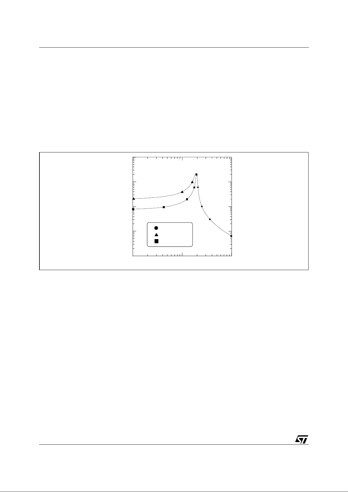
L6911C
f
S
f
200kHz
S
200kHz
⋅
4.306 10
---------------------------- -+=
R
k
T
⋅
15 10
--------------------+=
R
T
Ω()
Ω()
k
7
V
7
V
CC
CC
= 12V
= 5V
Switching frequency variations vs. R
µ
Note that forcing a 50
A current into this pin, the device stops switching because no current is delivered to the
are reported in Fig.1.
T
oscillator.
Figure 1.
10000
1000
100
Resistance [kOhm]
10
10 100 1000
RT to GN D
RT to VCC =12 V
RT to VCC =5V
Frequency [kHz]
Digital to Analog Converter
The built-in digital to analog converter allows the adjustment of the output voltage from 1.30V to 2.05V with
50mV binary steps and from 2.10V to 3.50V with 100mV binary steps as shown in the previous table 1. The
internal reference is trimmed to ensure the precision of 1%.
The internal reference voltage for the regulation is programmed by the voltage identification (VID) pins. These
are TTL compatible inputs of an internal DAC that is realized by means of a series of resistors providing a partition of the internal voltage reference. The VID code drives a multiplexer that selects a voltage on a precise
point of the divider. The DAC output is delivered to an amplifier obtaining the V
set-point of the error amplifier). Internal pull-ups are provided (realized with a 5
voltage reference (i.e. the
PROG
µ
A current generator); in this
way, to program a logic "1" it is enough to leave the pin floating, while to program a logic "0" it is enough to short
the pin to GND.
The voltage identification (VID) pin configuration also sets the power-good thresholds (PGOOD) and the overvoltage protection (OVP) thresholds.
The VID code "11111" disable the device (as a short on the SS pin) and no output voltage is regulated.
Soft Start and Inhibit
At start-up a ramp is generated charging the external capacitor CSS by means of a 10µA constant current, as
shown in figure 1.
When the voltage across the soft start capacitor (V
6/20
) reaches 0.5V the lower power MOS is turned on to dis-
SS

L6911C
charge the output capacitor. As VSS reaches 1V (i.e. the oscillator triangular wave inferior limit) also the upper
MOS begins to switch and the output voltage starts to increase.
The V
creases, as shown in figure 2. In this phase the system works in open loop. When V
clamp on the output of the error amplifi er is released. In any case another cla mp on the input of the err or amplifier remains active, allowing to V
In this second phase the system works in closed loop with a growing reference. As the output voltage reaches
the desired value V
increases until a maximum value of about 4V.
The Soft-Start will not take place, and the relative pin is internally shorted to GND, if both VCC and OCSET pins
are not above their own turn-on thresholds . During normal operation, if any under -voltage is detected on one of
the two supplies, the SS pin is internally shorted to GND and so the SS capacitor is rapidly discharged.
The device goes in INHIBIT state forcing SS pin below 0.4V. In this conditi on both external MOSFETS are kept
off.
Figure 2. Soft Start
growing voltage initially clamps the output of the error amplifier, and consequently V
SS
to grow with a lower slope (i.e. the slope of the VSS voltage, see figure 2).
OUT
, also the clamp on the error amplifier input is removed, and the soft start finishes. Vss
PROG
is equal to V
SS
linearly in-
OUT
COMP
the
Vcc
Vin
Vss
LGATE
Vout
to GND
Vcc Tu rn-on thresh o l d
Vin Turn-on threshold
1V
0.5V
Timing Diagram
Aquisition: CH1 = PHASE; CH2 = V
CH3 = PGOOD; CH4 = V
SS
OUT
;
Driver Section
The driver capability on the high and low side drivers allows using different types of power MOS (also multiple
MOS to reduce the R
), maintaining fast switching transition.
DSON
The low-side mos driver is supplied directly by Vcc while the high-side driver is supplied by the BOOT pin.
Adaptative dead time control i s implemented to pr event cross-c onduction and allow to use several kinds o f mos-
fets. The upper mos turn-on is avoided if the lower gate is over about 200mV while the lower mos turn-on is
avoided if the PHASE pin is over about 500mV. The upper mos is in any case turned-on after 200nS from the
low side turn-off.
The peak current is shown for both the upper ( fig. 3) and the lower (f ig. 4) driver at 5V and 12V. A 4nF capacitive
load has been used in these measurements.
For the lower driver, the source peak current is 1.1A @ Vcc=12V and 500mA @ Vcc=5V, and the sink peak
current is 1.3A @ Vcc=12V and 500mA @ Vcc=5V.
Similarly, for the upper driver, the source peak current is 1.3A @ Vboot-Vphase=12V and 600mA @ VbootVphase =5V, and the sink peak current is 1.3A @ Vboot-Vphase =12V and 550mA @ Vboot-Vphase = 5V.
7/20

L6911C
Figure 3. High Side driver peak current. Vboot-Vphase=12V (left) Vboot-Vphase=5V (right)
CH1 = High Side Gate CH4 = Gate Current
Figure 4. Low Side driver peak current. Vcc=12V (left) Vcc=5V (right)
CH1 = Low Side Gate CH4 = Gate Current
Monitoring and Protections
The output voltage is monitored by means of pin 1 (VSEN). If it is not w ithin ±12% (typ.) of the programm ed
value, the powergood output is forced low.
The device provi des ov ervoltage pr otection, when the output voltage reache s a value 17% (typ.) gr ater than the
nominal one. If the output voltage exceeds this threshol d, the OVP pin is fo rced high, triggerin g an external SCR
to shuts the supply (VIN) down, and also the lower driver is turned on as long as the over-voltage is detected.
To perform the overcurrent protection the device compares the drop across the high side MOS, due to the
RDSON, with the voltage across the external resistor (ROCS) connected between the OCSET pin and drain of
the upper MOS. Thus the overcurrent threshold (I
Where the typical value of I
R
(also the variation with temperature) and the minimum value of I
DSON
8/20
is 200µA. To calculate the ROCS value it must be considered the maximum
OCS
) can be calculated with the following relationship:
P
⋅
I
OCSROCS
-------------------------------- -=
I
P
R
DSON
. To avoid undesirable trigger of
OCS

L6911C
overcurrent protection this relationship must be satisfied:
∆
l
---- -+≥
=
IPI
OUTMAX
∆
Where
I is the inductance ripple current and I
OUTMAX
is the maximum output current.
In case of output short circuit the soft start capacitor is discharged with constant current (10
the SS pin reaches 0.5V the soft start phase is restarted. During the soft start the over-current protection is always active and if such kind of event occurs, the device turns off both mosfets, and the SS capacitor is discharged again (after reaching the upper threshold of about 4V). The system is now working in HICCUP mode,
as shown in figure 5a. After removing the c ause of the over-current, the device restart w orking normal ly w ithout
power supplies turn off and on.
Figure 5.
I
PEAK
2
µ
A typ.) and when
a: Hiccup Mode
9
8
7
6
5
4
3
2
Inductor Ripple [A]
1
0
0.5 1.5 2.5 3.5
Output Voltage [V ]
b: Indu ctor Ripple Current vs. Vout
L=1.5µH, Vin=12V
L=3µH, Vin=5V
L=2µH,
Vin=12V
L=3µH,
Vin=12V
L=1.5µH,
Vin=5V
L=2µH,
Vin=5V
Inductor design
The inductance value is defined by a compromise between the transient response time, the efficiency, the cost
and the size. The inductor has to be calculated to sustain the output and the input voltage variation to maintain
the ripple current
culated with this relationship:
Where f
SW
the ripple current vs. the output voltage for different values of the inductor, with V
∆
IL between 20% and 30% of the maximum output current. The inductance value can be cal-
–
L
V
INVOUT
------------------------------
∆
⋅
f
S
V
OUT
-------------- -
⋅=
I
V
L
IN
is the switching frequency, VIN is the input voltage and V
is the output voltage. Figure 5b shows
OUT
= 5V and VIN = 12V.
IN
Increasing the value of the inductance reduces the ripple current but, at the same time, reduces the converter
response time to a load transient. If the compensation network is well designed, the device is able to open or
close the duty cycle up to 100% or down to 0%. The response time is now the time required by the inductor to
change its current from initial to final value. Since the ind uctor has not fini shed its char ging tim e, the output current is supplied by the output capacitors. Minimizing the response time can minimize the output capacitance
required.
The response time to a load transient is different for the application or the removal of the load: if during the application of the loa d the inductor is c harged by a voltage equal to the difference between the input and the output
voltage, during the removal it is discharged only by the output voltage. The following expressions give approximate response time for
∆
I load transient in case of enough fast compensation network response:
9/20

L6911C
t
applicatio n
⋅
L∆I
----------------------------- -=
–
V
INVOUT
t
removal
⋅
L∆I
-------------- -=
V
OUT
The worst condition depends on the input voltage available and the output voltage selected. Anyway the worst
case is the response ti me after r emoval o f the load with the minimum output voltage programmed and the maximum input voltage available.
Output Capacitor
Since the microprocessors require a current variation beyond 10A doing load transients, with a slope in the
range of tenth A/
µ
sec, the output capacitor is a basic component for the fast response of the power supply. In
fact for first few microseconds they supply the current to the load. The controller recognizes immediately the
load transient and sets the duty cycle at 100%, but the current slope is limited by the inductor value.
The output voltage has a first drop due to the current variation inside the capacitor (neglecting the effect of the
ESL):
∆
V
OUT
= ∆I
OUT
· ESR
A minimum capacitor value is required to sustain the current during the load transient without discharge it. The
voltage drop due to the output capacitor discharge is given by the following equation:
2
∆
I
L
OUT
–⋅()⋅⋅
Where D
∆
V
OUT
is the maximum duty cycle value that is 100%. The lower is the ESR, the lower is the output drop
MAX
---------------------------------------------------------------------------------------------=
2C
OUTVINMINDMAXVOUT
during load transient and the lower is the output voltage static ripple.
Input Capacitor
The input capacitor has to sustain the ripple current produced during the on time of the upper MOS, so it must
have a low ESR to minimize the losses. The rms value of this ripple is:
I
rmsIOUT
–()⋅=
D1D
Where D is the duty cycle. The equation reaches its maximum value with D=0.5. The losses in worst case are:
2
P ESR I
⋅=
rms
Compensation network design
The control loop is a voltage mode (figure 7) that uses a droop function to satisfy the requirements for a VRM
module, reducing the size and the cost of the output capacitor.
This method "recovers" part of the drop due to the output capacitor ESR in the load transient, introducing a dependence of the output voltage on the load current: at light load the output voltage will be higher than the nominal level, while at high load the output voltage will be lower than the nominal value.
10/20

L6911C
Figure 6. Output transient response without (a) and with (b) the droop function
ESR DROP ESR DROP
V
MAX
V
V
NOM
V
MIN
(a) (b)
As shown in figure 6, the ESR drop is pr esent in any c ase, but using the droop func tion the total deviation of the
output voltage is minimized. In practice the droop function introduces a static error (Vdroop in figure 6) proportional to the output current. Since a sense resistor is not present, the output DC current is measured by using
the intrinsic resistance of the inductance (a few m
Ω
). So the low-pass filtered inductor voltage (that is the inductor current) is added to the feedback signal, implementing the droop function in a simple way. Referring to the
schematic in figure 7, the static characteristic of the closed loop system is:
⋅
R 8 // R9
V
OUT
V
PROGVPROG
+
R3 R8 // R9
-------------------------------------
R2
R
L
---------------------------------- -
R8
⋅–⋅+=
I
OUT
DROOP
Where V
resistance. The second term of the equation allows a positive offset at zero load (
the droop effect (
is the output voltage of the di gital to ana log conv erter (i .e. the set po int) and RL is the inductance
PROG
∆
V
). Note that the droop effect is equal the ESR drop if:
DROOP
⋅
R8 // R9
R
L
---------------------------------- -
R8
=
ESR
∆
V+); the third term introduces
Figure 7. Compensatio n ne tw o rk
V
IN
V
COMP
C18
R9
C25
R
L
V
PWM
Z
F
C20 R4
R3
PROG
V
R2
PHASE
Z
I
L2
R8
V
OUT
ESR
C6-15
Considering the previous relationships R2, R3, R8 and R9 may be determined in order to obtain the desired
droop effect as follow:
■
Choose a value for R2 in the range of hundreds of KΩ to obtain realistic values for the other
components.
11/20

L6911C
■
From the above equations, it results:
R8
=
R9 R8
+
∆
⋅
V
R2
-----------------------
V
PROG
∆
V
DROOP
-------------------------- -
⋅⋅
⋅
R
LIMAX
⋅
R
LIMAX
-------------------------- -
⋅=
∆
V
DROOP
1
------------------------------------ -
∆
V
DROOP
-------------------------- -+
1
⋅
R
LIMAX
;
;
Where I
■
The component R3 must be chosen in order to obtain R3<<R8//R9 to permit these and successive
is the maximum output current.
MAX
simplifications.
Therefore, with the droop function the output voltage decreases as the load current increases, so the DC output
impedance is equal to a resistance R
. It is easy to verify that the output voltage deviation under load tran-
OUT
sient is minimum when the output impedance is constant with frequency.
To choose the other components of the compensation network, the transfer function of the voltage loop is con-
sidered. To simplify the analysis is supposed that R3 << Rd, where Rd = (R8//R9).
Figure 8. Compensatio n ne tw o rk def i ni t io n
|Av |
2
|R|
R
|Gloop |
G
f
LC
0
D
f
0
2
f
f
CE
1
f
f
ECfCC
3
f
f
f
fc
f
⋅⋅=
π
CRfingularityonNetworkSCompensati
2/1
⋅=
π
fingularityConverterS
LC
f
CE
f
EC
f
CC
⋅⋅=
π
CESR
2/1
π
2/1
π
2/1
OUT
⋅⋅=
⋅⋅=
doublepoleLC
ESRzero
1
byIntroducedCceramicESR
acitorCeramicCapCceramicRceramic
2
3
f
d
2042/1
π
π
π
⋅+⋅=
CRRf
20)43(2/1
⋅⋅=
CRf
2532/1
⋅⋅=
CRd
252/1
The transfer function may be evaluated neglecting the connection of R8 to PHASE because, as will see later,
this connection is important only at low frequencies. So R4 is considered connected to VOUT. Under this assumption, the voltage loop has the following transfer function:
12/20

Gloop s()Av s()Rs
()⋅
()
Av s
()
Zf s
------------- -
⋅==
()
Zi s
Where
()
Av s
Vin
--------------- -
∆
V
osc
()
s
Z
C
------------------------------------ -
⋅=
s()ZLs
Z
C
L6911C
()+
Where Z
The expression of Z
Where:
(s) and ZL(s) are the output capacitor and inductor impedance respectively.
C
(s) may be simplified as follow:
I
==
()
s
Z
I
τ
= R4×C20,
1
1
-- -
⋅⋅
Rd
--------------------------------- -
Rd
C25
s
1
-- -+
⋅
C25
s
τ
= (R4+R3)×C20 and
2
1
-- -
R4
----------------------------------------------------- -+
R4
⋅+
s
1
-- -
⋅+
s
=
Rd
⋅
C20
C20
-------------------------------------------------------------------- -
R3
+
R3
------- - τ
1s
R
1s
τ
= Rd×C25.
d
R3
⋅+
d
⋅+()
τ
2
Rd 1 s
-------------------------------------------------------------------------------------------------- -
⋅+()⋅
1s
d
τ
⋅+()⋅
1s
τ
1τd
1s
τ
1
d
+()
⋅+()
τ
2
2
R3
------- -
⋅⋅⋅+⋅+
s
1s
τ
1τd
R
d
τd⋅+()⋅
=
The regulator transfer function became now:
()
Rs
------------------------------------------------------------------------------------------------------- -
≈
sC18R
1s
2
R3
------- -
1s
d
R
⋅+()
τ
Figure 8 shows a method to select the regul ator components (pleas e note that the fr equencies f
1s
⋅+
τ
d
d
⋅+()⋅
τ
d
⋅+()⋅⋅⋅ ⋅
1s
τ
1
and fCC cor-
EC
responds to the singularities introduced by additional ceramic capacitors in parallel to the output main electrolytic capacitor).
■
To obtain a flat frequency response of the output impedance, the droop time constant
τ
has to be equal
d
to the inductor time constant (see the note at the end of the section):
L
τ
d
■
To obtain a constant -20dB/dec Gloop(s) shape the singularity f1 and f2 are placed in proximity of fCE
and f
respectively. This implies that:
LC
⋅
RdC25
f
2
----
f
1
f1 f
■
To obtain a Gloop bandwidth of fC, results:
G0f
⋅ 1f
LC
=== ==
⇒⋅ A
C
G
⋅
0
0R0
------ - τ
R
L
f
LC
-------- -
R4⇒R3
f
CE
C20
CE
C20 // C25
VIN
⋅
----------------- -
Vosc∆
-----------------------------
L
C18
⇒
C25
f
LC
-------- -1–
⋅==
f
CE
1
-- - π
R4 f
2
f
C
C18⇒
------- -
f
LC
L
-----------------------=== =
⋅()
R
LRd
⋅⋅⋅=⇒=
CE
----------------- -
Vosc∆
-----------------------------
C20 C25
+
C20 C25⋅
VIN
⋅⋅
f
------- -
f
LC
C
Note.
To understand the reason of the previous assumption, the scheme in figure 9 must be considered.
In this scheme, the inducto r current has been subs tituted by the l oad current, becaus e in the fr equenci es range
of interest for the Droop function these current are substantially the same and it was supposed that the droop
network don't represent a charge for the inductor.
13/20

L6911C
E
Figure 9. Voltage regulation with droop function block scheme
LOOP
VoutVcomp
1
R
⋅
OUT
1
R
OUT
s
τ
⋅+
L
s
τ
⋅+
d
⋅== =
+
τ
1s
-----------------+
τ
1s
Iout
L
d
It results:
Z
OUT
V
o
--------------- -
I
LOAD
Av(s)
R(s)
+
τ
1s
L
------------------
⋅⋅
R
d
+
τ
1s
d
G
LOOP
---------------------------- +
1G
Because in the interested range |Gloop|>>1.
To obtain a flat shape, the relationship considered will naturally follow.
Demo Board Description
The L6911C demo board shows the operation of the device in a standard VRM 8.4 application. This evaluation
board allows voltage adjustability (1.3V - 3.5V) through the switches S1-S5 and high output current capability
(up to 14A). The device is supplied by the 12V input rail while the power conversion starts from the 5V input rail.
The device is also able to operate with a 5V supply voltage; in this case 12V input can be directly connected to
the 5V power source. The four layers demo board's c opper thickness is of 70
µ
m in order to minimi ze conduction
losses considering the high current that the circuit is able to deliver. Figure 10 shows the demo board's schematic circuit.
Figure 10. Demo Board Schematic
L1
F1
+5 VIN
14/20
GNDIN
+12Vcc
GND12
Q8
D1
BOOT
15
C17
S1
S2
S3
S4
S5
C16
VCC
18
GND
11
VID0
4
VID1
5
VID2
VID3
VID4
OSC
R1
6
L6911C
7
8
SS
3
20
9
COMP
U1
C18
C19
R5
G1
C24
OVP
19
OCSET
2
UGATE
14
PHASE
13
LGATE
17
PGND
16
PGOOD
12
VSEN
1
10
VFB
R3
C20
R2
C23
R7
R13
Q1-2
R14
Q4-5
R4
C21-22
D2
C1-5
L2
C6-15
R8
R9
C25
VOUTCOR
R12
GNDCORE
PWRGD
L6911-L6912 EVALUATION KIT REV.

L6911C
Efficiency
Figure 11 shows the m easured effi ciency versu s load current for different values of ou tput vol tage. The measure
was done at Vin=5V for different values of the output voltage (2.05V and 2.75V). Two different measurements
were done using IC supply voltage of 5V and 12V.
In the application two mosfets STS12NF30L (30V, 10m
both the low and the high side.
The board has been layed out with the possibility to use up to three SO8 mosfets for both high and low side
switch. Two D
2
PACK mosfets (one for each high and low side) may also be used in order to allow the maximum
flexibility in meeting different requirements.
Figure 11. Efficiency vs. load
95
90
85
80
75
70
Efficiency [%]
65
60
55
0 2 4 6 8 10 12 14 16
Vout = 1.7V
Vout = 2.0V
Vout = 2.5V
Output Current [A]
Ω
typ @ Vgs=4.5V) connected in parallel are used for
95
90
85
80
75
70
Efficiency [%]
65
60
55
0 2 4 6 8 10 12 14 16
Vou t = 1.7V
Vou t = 2.0V
Vou t = 2.5V
Output Current [A]
Vcc = 12V; Vin = 5V Vcc = Vin = 5V
Load Transient Response
Figure 12 shows the demo board response to a load
transient application. The load transient applied
changes from 0A to 14A on the output current (Channel 4). It may be observed that output vol t age (Channel 1) remains within the 100mV toler ance across the
regulated voltage. Figure 13 shows details about the
the circuit response during current rising and falling
edge; it is possible to observe that the duty cycle of
the Phase signal (Channel 2) goes up to 100% or
down to 0% if necessary.
Figure 12. Load Transient Response
Figure 13. Load Transient Response Details
15/20

L6911C
Inductor selection
Since the maximum output current is equal to 14A, to have a 30% ripple (4A) in worst case a 3µH inductor has
been chosen. So the ripple is 4.1A @ 3.5V with V
In worst case the peak is equal to 18.1A.
Output Capacitor
In the demo ten Sanyo capacitors, model 6MV1000GX are used, with a maximum ESR equal to 69mΩ. Therefore, the resultant ESR is 69m
Ω
/10 = 1.9mΩ. For a load transient of 14A in worst case the drop results:
∆
Vout = 14 * 0.00069 = 96.6mV
The voltage drop due to the c apacitor di scharge duri ng load transient, consi deri ng that the maxi mum duty cyc le
is equal to 100% results in 13mV with 2.5V of programmed output.
Input Capacitor
For I
= 14A and D = 0.5 (worst case for input ripple current), Irms is equal to 7A. Five Sanyo electrolytic
OUT
capacitors 25MV330GX, with a maximum ESR equal to 69m
resultant ESR is equal to 69m
Ω
/5 = 13.8mΩ. So the losses in worst case are:
==
P ESR I
Over-Current Protection
Substituting the demo board parameters in the relationship reported in the relative section, (I
I
= 19A; R
P
DSONMAX
= 9mΩ) it results that R
=12V and 1.7A @ 3.5V with VIN = 5V.
IN
Ω
, are chosen to sustain the ripple. Therefore, the
2
OCS
⋅
rms
= 1kΩ.
670mW
OCSMIN
= 170µA;
Part List
R2 499k 1% SMD 0805
R3, R7 1k 1% SMD 0805
R4 20 SMD 0805
R5, R8 20k SMD 0805
R9 15k SMD 0805
R12 1K SMD 0805
R13, R14 0 SMD 0805
C1, C2…C5
C6, C7…C15 1000µ SANYO – 6MV1000GX Radial 8x20mm
C16, C17, C24, C25 100n Ceramic SMD 0805
C18 2.2n Ceramic SMD 0805
C19 8.2n Ceramic SMD 0805
C20 82n Ceramic SMD 0805
C21, C22 1µ Ceramic SMD 1206
C23 1n Ceramic SMD 0805
L1
L2 3µ T50-52B Core, 10T-16AWG
U1 L6911C STMicroelectronics SO20
Q1, Q2…Q6 STS12NF30L STMicroelectronics SO8
D1 1N4148 STMicroelectronics SOT23
D2 STPS3L25U STMicroelectronics SMB
F1 251015A-15° Littlefuse AXIAL
µ SANYO – 25MV330GX Radial 8x20mm
330
µ T44-52 Core, 7T-18AWG
1.5
16/20

PCB AND COMPONENTS LAYOUTS
Figure 14. PCB and Components Layouts
Component Side Internal Ground Plane
Figure 15. PCB and Components Layouts
L6911C
Internal Layer Solder Side
17/20

L6911C
Application Circuit Examples
Figure 16 reports the schematic circuit for a motherboard chipset power supply. This application works from a
single 5V power supply and is able to deliver up to 10A with a 300KHz switching frequency.
Figure 16. Motherboard chipset power supply; 2.5Vout, 10A
+5 VIN
GNDIN
CoilCraft DO3316P
10A fuse
1uH
100nF
100n
3x220uF
43k
1N4148
VCC
GND
VID0
VID1
VID2
VID3
VID4
SS
OSC
15
18
11
4
5
6
L6911C
7
8
3
20
9
COMP
BOOT
680pF
U1
220pF
100k
750k
100n
OVP
19
OCSET
2
UGATE
14
PHASE
13
LGATE
17
PGND
16
PGOOD
12
VSEN
1
10
VFB
10k
5.6n
220
STS12NF 30L
STS12NF 30L
1n
1k
2x1uF
ceramic
CoilCraft DO5022P
1.5uH
STPS3L25U
Sanyo
5x470uF
10k
Sanyo TP B
VOUTCORE
GNDCORE
PWRGD
18/20

L6911C
DIM.
MIN. TYP. MAX. MIN. TYP. MAX.
A 2.35 2.65 0.093 0.104
A1 0.1 0.3 0.004 0.012
B 0.33 0.51 0.013 0.020
C 0.23 0.32 0.009 0.013
D 12.6 13 0.496 0.512
E 7.4 7.6 0.291 0.299
e 1.27 0.050
H 10 10.65 0.394 0.419
h 0.25 0 .75 0.010 0.030
L 0.4 1.27 0.016 0.050
K 0˚ (min.)8˚ (max.)
mm inch
OUTLINE AND
MECHANICAL DATA
SO20
B
e
D
1120
110
L
h x 45˚
A
K
A1
C
H
E
SO20MEC
19/20

L6911C
Information furnished is believed to be accurate and reliable. However, STMicroelectronics assumes no responsibility for the consequences
of use of such information nor for any infringement of patents or other rights of third parties which may result from its use. No license is granted
by implic ation or otherwise under any patent or p at ent rights of STMicroelectronics. Spec i fications mentioned i n this publication are subject
to change without notice. This publication supersedes and replaces all information previously supplied. STMicroelectronics products are not
authorized for use as cri t i cal compone nts in life support device s or systems without express written approval of STMicroel ectronics.
The ST logo is a registered trademark of STMicroelectronics
2001 STMi croelectronics - All Ri ghts Rese rved
Australi a - Brazil - Chin a - Finland - Franc e - Germany - Hong Kong - India - Ita l y - Japan - Malaysi a - Malta - Morocco - Singapore - Spain
STMicroelectronics GROUP OF COMPANIES
- Sweden - Sw itzerlan d - United Kin gdom - U.S.A.
http://www.s t. com
20/20
 Loading...