

查询L6911供应商
5 BIT PROGRAMMABLE POWER SUPPLY
CONTROLLERFOR PENTIUM II PROCESSOR
OPERATING SUPPLY VOLTAGE FROM 5V
TO 12V
TTL-COMPATIBLE 5BIT PROGRAMMABLE
OUTPUTFROM:
-1.3V TO 2.05VWITH0.05V BINARYSTEPS
-2.1V TO 3.5V WITH0.1V BINARYSTEPS
VOLTAGEMODEPWM CONTROL
EXCELLENT OUTPUT ACCURACY +/-1%
OVERLINE,ANDTEMPERATUREVARIA T IO NS
HIGH PRECISION INTERNAL REFERENCE
DIGITALLY TRIMMED
VERYFAST LOAD TRANSIENT0% TO 100%
DUTY CYCLE
POWERGOOD OUTPUT
OVERVOLTAGE PROTECTION
OVERCURRENT PROTECTION REALISED
USING THE MOSFET’sR
OPERATINGFREQUENCY FROM 50KHz TO
1MHz
MEETSINTEL PENTIUM II SPECIFICATION
DISABLEFUNCTION
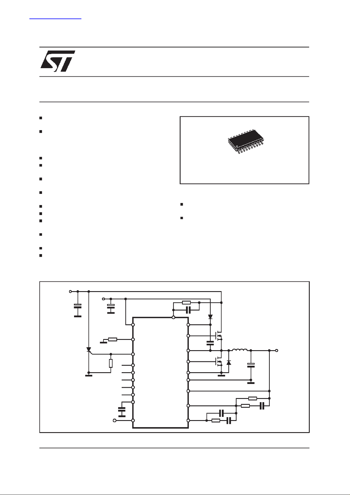
APPLICATIONCIRCUIT
DSon
L6911B
SO20
Applications
POWER SUPPLY FOR ADVANCED MICROPROCESSORSUPPLIES
POWER SUPPLY FOR PENTIUM II INTEL
PROCESSORS
DESCRIPTION
The L6911B is a power supply controller specifically designed to provide a high performance
DC/DC conversion for Pentium II Microprocessors. A precise 5 bit digital to analog converter
April 1999
Vin 5V/12V
V
5V/12V
CC
VCC
OSC
OVP
VD0
VD1
VD2
VD3
VD4
SS
PGOOD 12
OCSET
18
20
19
4
5
6
7
8
3
2
BOOT
15
UGATE
14
Vo
13
PHASE
17
LGATE
16
PGND
11
GND
1
VSEN
VFB
10
COMP
9
1.3V to 3.5V
D98IN956B
1/7
L6911B
DESCRIPTION(continued)
(DAC) allows to adjust the output voltage from
1.3V to 2.05V with 0.05V binary steps and from
2.1V to 3.5V with 0.1V binary steps. The high precision internal reference, digitally trimmed, assures the selected output voltage to within +/-1%.
Thanks to thewindow comparatorsystem,the device provides excellent load transient performance. The high peak current gate drive affords to
ABSOLUTEMAXIMUMRATINGS
Symbol Parameter Value Unit
V
CC
V
BOOT-VPHASE
VCCto PGND 15 V
Boot Voltage 15 V
Input, Output or I/O Voltage -0.3 to V
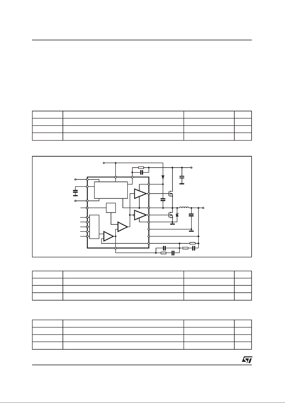
BLOCK DIAGRAM
V
12V
CC
have fast switching to the external power mos,
performing an high efficiency. The L6911B assures a fast protection against load overvoltage
and load overcurrent. An external SCR is triggered to crowbar the input supply in case of overvoltage. In case of output short circuit the soft
start capacitor is discharged and the system
works inhiccup mode.
+0.3 V
CC
Vin 5V
PGOOD
OVP
VD0
VD1
VD2
VD3
VD4
D98IN957A
SS
RT
D/A
VCC OCSET
MONITOR and
PROTECTION
OSC
+
E/A
COMP
BOOT
UGATE
PHASE
LGATE
-
+
PWM
PGND
GND
VSEN
VFB
Vo
1.8V to 3.5V
THERMAL DATA
Symbol Parameter Value Unit
R
thj-amb
T
T
max
stg
Thermal Resistance Junction to Ambient 110 °C/W
Maximum Junction Temperature 150 °C
Storage Temperature Range -65 to 150 °C
RECOMMENDED OPERATINGCONDITION
Symbol Parameter Value Unit
2/7
V
CC
T
amb
T
J
VCCto PGND 5V±10%/12V±10% V
Ambient Temperature Range 0 to 70 °C
Junction Temperature Range 0 to 125 °C
PIN CONNECTION
L6911B
VSEN
OCSET
SS
VID0
VID1
VID2
VID3
VID4
COMP PGOOD
FB GND
2
3
4
5
6
7
8
9
10
D98IN958
20
19
18
17
16
15
14
13
12
11
RT1
OVP
VCC
LGATE
PGND
BOOT
UGATE
PHASE
PIN FUNCTIONS
N° Name Description
1 VSEN Connected to the output voltage is able to manage overvoltage conditions and the PGOOD
2 OCSET A resistor connected from this pin and the upper Mos Drain sets thecurrent limit protection.
3 SS The soft starttime is programmed connecting an external capacitor from this pin and GND.
4 - 8 VID0 - 4 Voltage Identification code pins. These input are open collector and TTL compatible. Are used
9 COMP This pin is connected to the error amplifier output and is used to compensate the voltage
10 FB This pin is connected to the error amplifier inverting inputand is used to compensate the
11 GND All internal voltage reference are referred to this pin.
12 PGOOD This pin is an open collectoroutput and is pulled low if the output voltage is not within±10%
13 PHASE This pin is connected to the source of the upper mosfet and provides the return pathfor the
14 UGATE High side gate driver output.
15 BOOT Bootstrap capacitor pin. Through this pin is supplied the high side driver and the upper mosfet.
16 PGND Power ground pin. This pin has to be connected closely to the low side mosfet source in order
17 LGATE This pin is the lower mosfet gate driver output.
18 VCC Device supply voltage. The operative supply voltage range is 4.5V to 12V.
19 OVP Over voltage protection. If the output voltage reach the 15% above the programmed voltage
signal.
The internal 200µA current generator sinks a currentfrom the drain through the external
resistor. The overcurrent threshold is due to the following equation:
I
⋅ R
ocs
I
=
P
ocs
Rdson
The internal current generator forces through the capacitor 10µA.This pin can be used to
disable the device forcing a voltage lower than 0.4V.
to program the output voltage as specified in Table 1 and to set the overvoltage and
powergood thresholds.
control feedback loop.
voltage control feedback loop.
of the programmed voltage. This pin is forced high if the ”11111” VID is set.
high side driver. This pin monitors the drop across the upper mosfet forthe current limit.
to reducethe noise injection into the device.
Do not connect V
to 12V if VCCis 5V.
IN
this pin is driven high and can be used to drive an external SCR that crowbar the supply
voltage.
3/7

L6911B
PIN FUNCTION(continued)
N° Name Description
20 RT Oscillator Switching frequency pin. Connecting an external resistorfrom this pin to ground the
ELECTRICALCHARACTERISTICS
Symbol Parameter Test Condition Min. Typ. Max. Unit
VCC SUPPLY CURRENT
I
CC
POWER-ON
OSCILLATOR
V
∆
osc
REFERENCE and DAC
ERROR AMPLIFIER
GBW Gain-Bandwidth Product - 15 - MHz
SR Slew Rate COMP = 10pF - 10 - V/µs
GATE DRIVERS
I
UGATE
R
UGATE
I
LGATE
R
LGATE
PROTECTION
I
OCSET
I
OVP
I
SS
Supply current UGATE and LGATE open - 5 - mA
Rising V
Falling V
Rising VOCSET Threshold - 1.26 - V
Free Running Frequency RT = open 185 200 215 kHz
Total Variation R
Ramp Amplitude RT = open - 1.9 - V
DACOUT voltage Accuracy VID0, VID1,VID2, VID3 see
DC Gain - 88 - dB
Upper Gate Source V
Upper Gate Sink I
Lower Gate Source VCC= 12V, V
Lower Gate Sink I
Overvoltage Trip
(V
OCSET Current Source V
OVP Sourcing Current V
Soft Start Current 10 µA
switching frequency is increased according to the equation:
6
10
f
S
200kHz
=
5⋅
+
R
(KΩ)
T
Connecting the resistor from this pin and the Vcc the Switching frequency is reduced
according to the equation:
7
10
f
= 200kHz −
S
4⋅
RT(KΩ)
If the pin is not connected the switching frequency is 200kHz.
Threshold VOCSET = 4.5V - - 4.6 V
CC
Threshold VOCSET = 4.5V 3.6 - - V
CC
to GND >6kΩ,
T
R
to VCC= 12V > 200kΩ
T
-15 - 15 %
-1 - 1 %
Table1
- Vphase = 12V,
BOOT
V
=6V
UGATE
= 0.3A - 1.5 3
LGATE
= 6V 1.2 2 - A
LGATE
= 0.3A - 1 2
LGATE
0.6 1 - A
- 115 120 %
/DACOUT)
SEN
= 4.5VDC 170 200 230
OCSET
SEN
= 5.5V, V
=0V 60 mA
OVP
Ω
Ω
A
µ
4/7

ELECTRICALCHARACTERISTICS (continued)
Symbol Parameter Test Condition Min. Typ. Max. Unit
Rising 106 - 111 %
V
SEN
Rising 89 - 94 %
V
SEN
Upper and Lower Threshold - 2 - %
= -5mA - 0.5 - V
PGOOD
V
PGOOD
Upper Threshold
/DACOUT)
(V
SEN
Upper Threshold
(V
/DACOUT)
SEN
Hysteresis
(V
/DACOUT)
SEN
PGOOD Voltage Low I
Table 1.
VID4 VID3 VID2 VID1 VID0 OUTPUT VOLTAGE (V)
01111 1.3
0 1 1 1 0 1.35
01101 1.4
0 1 1 0 0 1.45
01011 1.5
0 1 0 1 0 1.55
01001 1.6
0 1 0 0 0 1.65
00111 1.7
0 0 1 1 0 1.75
00101 1.8
0 0 1 0 0 1.85
00011 1.9
0 0 0 1 0 1.95
00001 2
0 0 0 0 0 2.05
11111 0
11110 2.1
11101 2.2
11100 2.3
11011 2.4
11010 2.5
11001 2.6
11000 2.7
10111 2.8
10110 2.9
10101 3
10100 3.1
10011 3.2
10010 3.3
10001 3.4
10000 3.5
L6911B
5/7

L6911B
DIM.
MIN. TYP. MAX. MIN. TYP. MAX.
A 2.35 2.65 0.093 0.104
A1 0.1 0.3 0.004 0.012
B 0.33 0.51 0.013 0.020
C 0.23 0.32 0.009
D 12.6 13 0.496 0.512
E 7.4 7.6 0.291 0.299
e 1.27 0.050
H 10 10.65 0.394 0.419
h 0.25 0.75 0.010 0.030
L 0.4 1.27 0.016 0.050
K0°(min.)8°(max.)
mm inch
0.013
OUTLINE AND
MECHANICAL DATA
SO20
B
e
D
1120
110
L
hx45°
A
K
A1
C
H
E
SO20MEC
6/7

L6911B
Information furnished is believed to be accurate and reliable. However, STMicroelectronics assumes no responsibility for the consequences
of use of such information nor for any infringement of patents or other rights of third parties which may result from its use. No license is
granted by implication or otherwise under any patent or patent rights of STMicroelectronics. Specification mentioned in this publication are
subject to change without notice. This publication supersedes and replaces all information previously supplied. STMicroelectronics products
are not authorized for use as critical components in lifesupport devices or systems without express written approval of STMicroelectronics.
The ST logo is a registered trademark of STMicroelectronics
1999 STMicroelectronics – Printedin Italy – All Rights Reserved
STMicroelectronics GROUP OF COMPANIES
Australia - Brazil - Canada - China - France - Germany - Italy - Japan - Korea - Malaysia - Malta - Mexico - Morocco - The Netherlands -
Singapore- Spain- Sweden- Switzerland - Taiwan - Thailand - United Kingdom- U.S.A.
http://www.st.com
7/7
 Loading...