

查询L6902D供应商
UP TO 1A SWITCHING REGULATOR WITH
■
UP TO 1A OUTPUT CURRENT
■
OPERATING INPUT VOLTAGE FROM 8V TO 36V
■
PRECISE 3.3V ( ±2%) REFE RENCE VOLTAGE
■
5% OUTPUT CURRENT ACCURACY
■
OUTPUT VOLTAGE ADJUSTABLE FROM
1.235V TO 34V
■
250KHz INTERNALLY FIXED FREQUENCY
■
VOLTAGE FEEDFORWA R D
■
ZERO LOAD CURRENT OPERATION
■
ADJUSTABLE CURRENT LIMIT
■
PROTECTION AGAINST FEEDBACK
DISCONNECTION
■
THERMAL SHUTDOWN
APPLICATION S
■
CHARGERS FOR NiCd, NiMH BATTERIES
AND PREREGULATOR FOR LITHIUM-ION
BATTERIES
■
ADJUSTABLE CURRENT GENERATOR
■
SIMPLE STEP-DOWN CONVERTERS WITH
ADJUSTABLE CURRENT LIMIT
■
BATTERY EQUIPPED SYSTEMS
■
DISTRIBUTED PO WE R SUPP LY
■
MOBILE PC & SUBNOTEBOOK
DESCRIPTION
The L6902D is a complete and simple step down
switching regulator with adjustable current limit.
Based on a voltage mode structure it integrates a cur-
L6902D
ADJUSTABLE CURRENT LIMIT
SO8
ORDERING NUMBERS: L6902D
L6902D013TR (Tape & Reel)
rent error amplifier to have a constant voltage and constant cu rrent control.
By means of an on board current sense resistor and
the availability of the current sense pins (both compatible to Vcc and for Cs- compatible with GND too)
a current limit programming is very simple and accurate (±5%). Moreover constant current control can be
used to charge NiMH and NiCd batteries.
The device can be used as a standard DC/DC converter with adjustable current limit (set by using the
external sense resistor).
The internal robust P-Channel DMOS transistor with a
typical of 250m
mum dropout even at high output current level. The internal limiting current (latched function) of typical value
of 2.5A protect s the device from accidental output short
circuit avoiding dangerous loads damage.
If the temperature of the chip goes hi gher than a fixed
internal threshold (150°C with 20°C hysteresis), the
power stage is turned off.
Ω
assures high efficiency and a mini-
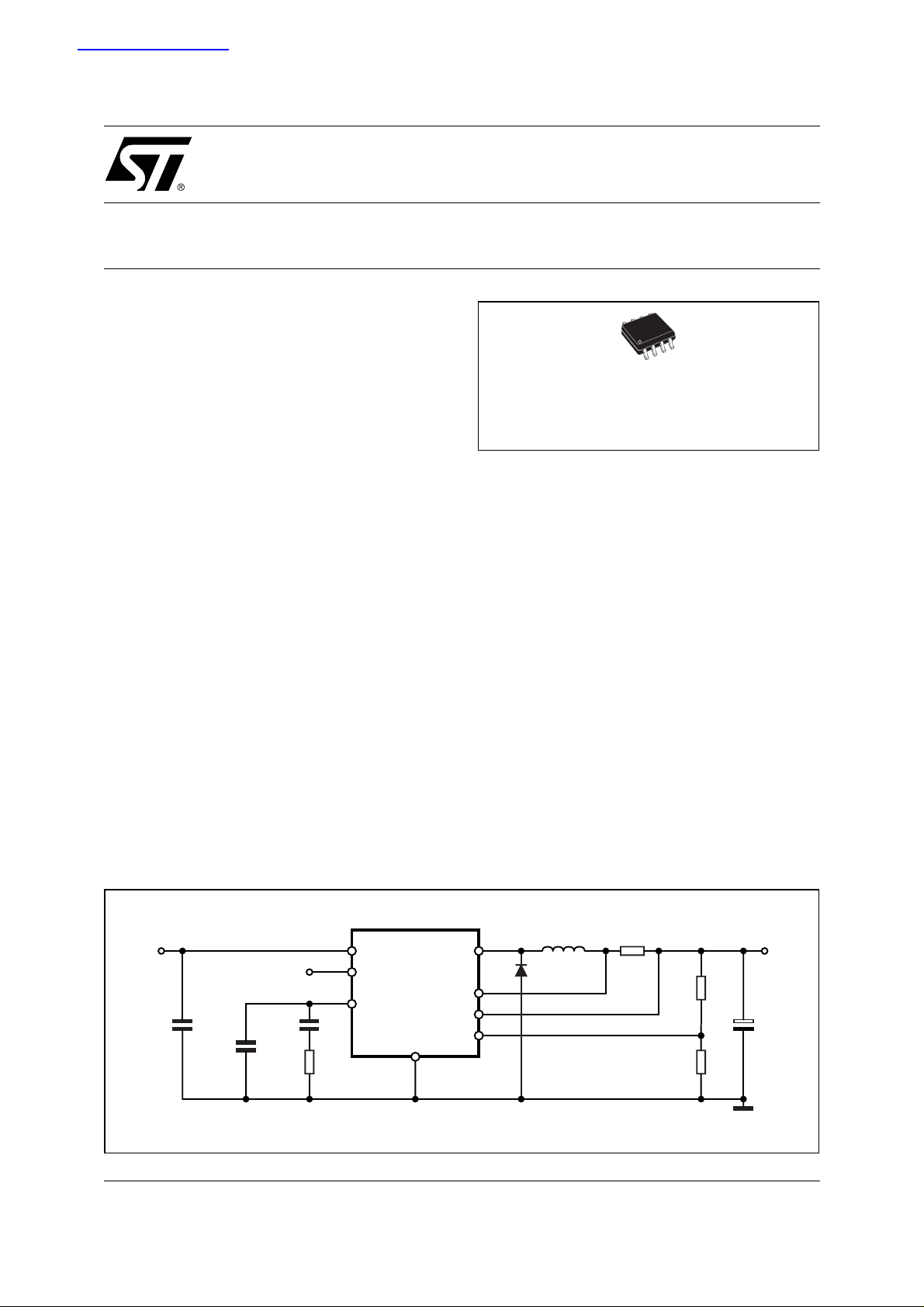
TEST AND APPLICATION CIRCUIT
=8V to 36V
V
IN
C1
10µF
25V
CERAMIC
June 2002
C3
220pF
D01IN1306A
3.3V
C2
22nF
R3
5.1K
CC
VREF
COMP
OUT
8
6
4
7
GND
1
2
3
FB
5
L1 22µH
D1
STPS340U
R
SENSE
100mΩ
R1
5.6K
R2
3.3K
V
OUT
POSCAP
=3.3VV
C4
100µF
10V
1/6

L6902D
DESCRIPTION
(Continued)
Other protections beside thermal shutdow n compl ete the device for a safe and r eli able appli cation: overv oltage
protection, frequency folback overcurrent protection and protection vs. feedback disconnection.
The internal fixed switching frequency of 250KHz, and the SO-8 package pin allow to built an ultra compact DC/
DC converter with a minimum board space.
PIN CONNECTION
OUT
CS+
CS-
COMP
1
2
3
4
8
7
6
5
VCC
GND
VREF
FB
PIN DESCRIPTION
N° Pin Function
1 OUT Regular Output
2 CS+ Current Error Amplifier input (current sense at higher voltage)
3 CS- Current Error Amplifier input (current sense at lower voltage)
4 COMP E/A output to be used for frequency compensation
5 FB Stepdown feedback input. Connecting directly to this pin results in an output voltage of 1.235V.
An external resistive divider is required for higher output voltages. In this case:
R1
V
==
outVFB
1
------- -+
⋅ 1.235V 1
R2
R1
------- -+
R2
6V
7 GND Ground
8 VCC Unregulated DC input voltage.
3.3V VREF. No cap is need for stability.
REF
THERMAL DATA
Symbol Parameter Value Unit
R
th j-amb
(*) Package mounted on board.
Thermal Resistance Junction to Ambient Max. 110 (*) °C/W
ABSOLUTE MAXIMUM RATINGS
Symbol Parameter Value Unit
V
V
I
1
, V
V
4
, V
V
2
P
tot
Tj Operating junction temperature range -40 to 150 °C
T
stg
Input Voltage 40 V
8
Output DC voltageOutput peak voltage at t = 0.1µs -1 to 40
1
Maximum output current Internally limited
Analog pins 4 V
5
Analog pins -0.3V to V
3
Power dissipation at T
Storage temperature range -55 to 150 °C
≤ 70 °C 0.7 W
amb
-5 to 40
CC
V
V
V
2/6
 Loading...