

Features
■ Dual MOSFET driver for synchronous rectified
converters
■ High driving current for fast external MOSFET
switching
■ Integrated bootstrap diode
■ High frequency operation
■ Enable pin
■ Adaptive dead-time management
■ Flexible gate-drive: 5 V to 12 V compatible
■ High-impedance (HiZ) management for output
stage shutdown
■ Preliminary overvoltage (OV) protection
■ VFDFPN8 3x3 mm package
Applications
■ High current VRM / VRD for desktop / server /
workstation CPUs
■ High current and high efficiency DC-DC
converters
Description
The L6747A is a flexible, high-frequency dualdriver specifically designed to drive N-channel
MOSFETs connected in synchronous-rectified
buck topology.
L6747A
High current MOSFET driver
VFDFPN8 3x3 mm
regulator solutions for modern high-current CPUs
and for DC-DC conversion in general.
The L6747A embeds high-current drivers for both
high-side and low-side MOSFETS. The device
accepts a flexible power supply of 5 V to 12 V.
This allows optimization of the high-side and lowside gate-drive voltage to maximize system efficiency.
The embedded bootstrap diode eliminates the
need for external diodes. Anti shoot-through management prevents the high-side and low-side
MOSFETs from conducting simultaneously and,
combined with adaptive dead-time control, minimizes the LS body diode conduction time.
The L6747A features preliminary OV protection to
protect the load from dangerous overvoltage due
to MOSFET failures at startup.
The L6747A device is available in a VFDFPN8
3x3 mm package.
Combined with ST PWM controllers, the driver
allows the implementation of complete voltage
Table 1. Device summary
Order code Package Packing
L6747A VFDFPN8 Tube
L6747ATR VFDFPN8 Tape and reel
March 2010 Doc ID 17126 Rev 1 1/15
www.st.com
15

Contents L6747A
Contents
1 Typical application circuit and block diagram . . . . . . . . . . . . . . . . . . . . 3
2 Pin information and thermal data . . . . . . . . . . . . . . . . . . . . . . . . . . . . . . 4
2.1 Pin information . . . . . . . . . . . . . . . . . . . . . . . . . . . . . . . . . . . . . . . . . . . . . . 4
2.2 Thermal data . . . . . . . . . . . . . . . . . . . . . . . . . . . . . . . . . . . . . . . . . . . . . . . 5
3 Electrical specifications . . . . . . . . . . . . . . . . . . . . . . . . . . . . . . . . . . . . . . 6
3.1 Absolute maximum ratings . . . . . . . . . . . . . . . . . . . . . . . . . . . . . . . . . . . . . 6
3.2 Electrical characteristics . . . . . . . . . . . . . . . . . . . . . . . . . . . . . . . . . . . . . . . 6
4 Device description and operation . . . . . . . . . . . . . . . . . . . . . . . . . . . . . . 8
4.1 High-impedance (HiZ) management . . . . . . . . . . . . . . . . . . . . . . . . . . . . . 9
4.2 Preliminary OV protection . . . . . . . . . . . . . . . . . . . . . . . . . . . . . . . . . . . . . 9
4.3 BOOT capacitance design . . . . . . . . . . . . . . . . . . . . . . . . . . . . . . . . . . . . . 9
4.4 Power dissipation . . . . . . . . . . . . . . . . . . . . . . . . . . . . . . . . . . . . . . . . . . . 10
4.5 Layout guidelines . . . . . . . . . . . . . . . . . . . . . . . . . . . . . . . . . . . . . . . . . . . 11
5 Package mechanical data . . . . . . . . . . . . . . . . . . . . . . . . . . . . . . . . . . . . 13
6 Revision history . . . . . . . . . . . . . . . . . . . . . . . . . . . . . . . . . . . . . . . . . . . 14
2/15 Doc ID 17126 Rev 1

L6747A Typical application circuit and block diagram
1 Typical application circuit and block diagram
Figure 1. L6747A typical application circuit
VCC = 5V to 12V
CDEC
VCC
BOOT
PWM Input
EN Input
L6747A Reference Schematic
PWM
EN
GND
UGATE
PHASE
L6747A
LGATE
Figure 2. L6747A block diagram
VCC
EN
70k
L6747A
HS
LS
CROSS CONDUCTION
ADAPTIVE ANTI
HS
VCC
VIN = 5V to 12V
C
HF
L
CBULK
Vout
COUT
BOOT
UGATE
10k10k
PHASE
PWM
7k
CONTROL LOGIC
& PROTECTIONS
Doc ID 17126 Rev 1 3/15
PWM
LS
LGATE
GND
Pin information and thermal data L6747A
2 Pin information and thermal data
2.1 Pin information
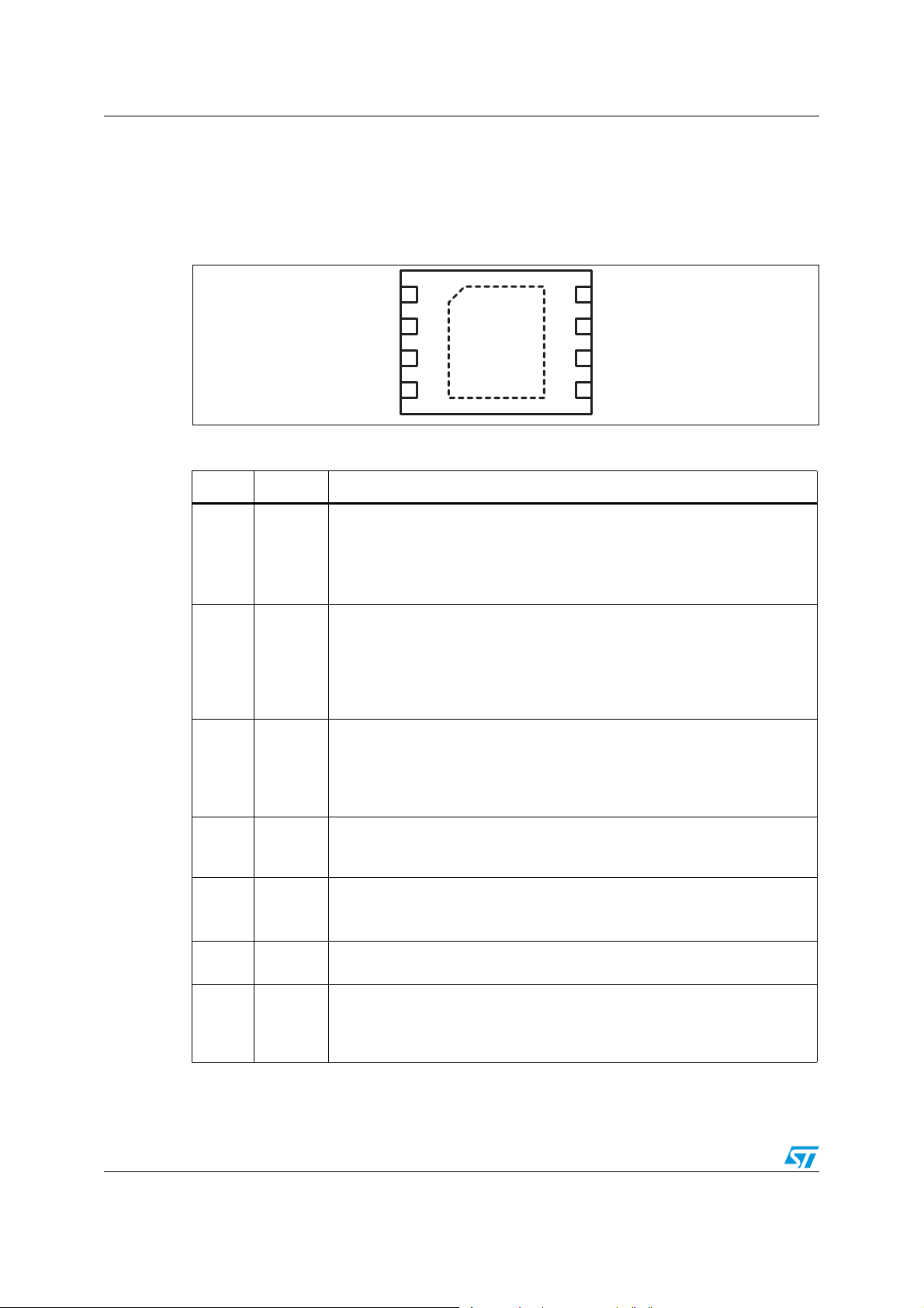
Figure 3. Pin connection diagram (top view)
BOOT
PWM
EN
VCC
Table 2. Pin descriptions
Pin # Name Function
High-side driver supply.
This pin supplies the high-side floating driver. Connect through a R
1BOOT
2PWM
3EN
(2.2Ω - 220nF typ.) network to the PHASE pin.
C
BOOT
Internally connected to the cathode of the integrated bootstrap diode.
See Section 4.3 for guidance in selecting the capacitor value.
Control input for the driver; 5V compatible, internally clamp to 3.3V.
This pin controls the state of the driver and which external MOSFET must be
turned ON according to EN status.
It manages the high-impedance (HiZ) state which sets all the MOSFETs to
OFF if externally set in the HiZ window (see Tab l e 5).
See Section 4.1 for details of HiZ.
Enable input for the driver; 5V compatible, internally clamp to 3.3V.
Pull high to enable the driver based on the PWM status.
Pull low to enter HiZ state with all MOSFETs OFF, regardless of the PWM
status.
See Section 4.1 for details of HiZ.
1
2
3
4
L6747A
8
7
6
5
UGATE
PHASE
GND
LGATE
BOOT
-
Device and LS driver power supply.
4VCC
5LGATE
6GND
7 PHASE
4/15 Doc ID 17126 Rev 1
Connect to any voltage between 5V and 12V.
Bypass with low-ESR MLCC capacitor to GND (1µF typ).
Low-side driver output.
Connect directly to the low-side MOSFET gate. A small series resistor may be
used to reduce dissipated power, especially in high frequency applications.
All internal references, logic and drivers are referenced to this pin. Connect to
the PCB ground plane.
High-side driver return path. Connect to the high-side MOSFET source.
This pin is also monitored for adaptive dead-time management and pre-OV
protection.
Internal clamp circuitry prevents leakage from this pin in disable conditions.

L6747A Pin information and thermal data
Table 2. Pin descriptions (continued)
Pin # Name Function
High-side driver output.
8UGATE
Connect to high-side MOSFET gate. A small series resistor may be used to
control the PHASE pin negative spike.
-TH. PAD
2.2 Thermal data
Table 3. Thermal data
Symbol Parameter Value Unit
R
R
T
T
P
THJA
THJC
MAX
STG
T
J
TOT
Thermal resistance junction-to-ambient
(device soldered on 2s2p, 67mm x 69mm board)
Thermal resistance junction-to-case 5 °C/W
Maximum junction temperature 150 °C
Storage temperature range 0 to 150 °C
Junction temperature range 0 to 125 °C
Maximum power dissipation at 25°C
(device soldered on 2s2p,67mm x 69mm board)
Thermal pad connects the silicon substrate and makes good thermal contact
with the PCB. Connect to the PGND plane.
45 °C/W
2.25 W
Doc ID 17126 Rev 1 5/15
 Loading...