

Features
■ Dual MOSFET driver for synchronous rectified
converters
■ High driving current for fast external MOSFET
switching
■ Integrated bootstrap diode
■ High frequency operation
■ Enable pin
■ Adaptive dead-time management
■ Flexible gate-drive: 5 V to 12 V compatible
■ High-impedance (HiZ) management for output
stage shutdown
■ Preliminary OV protection
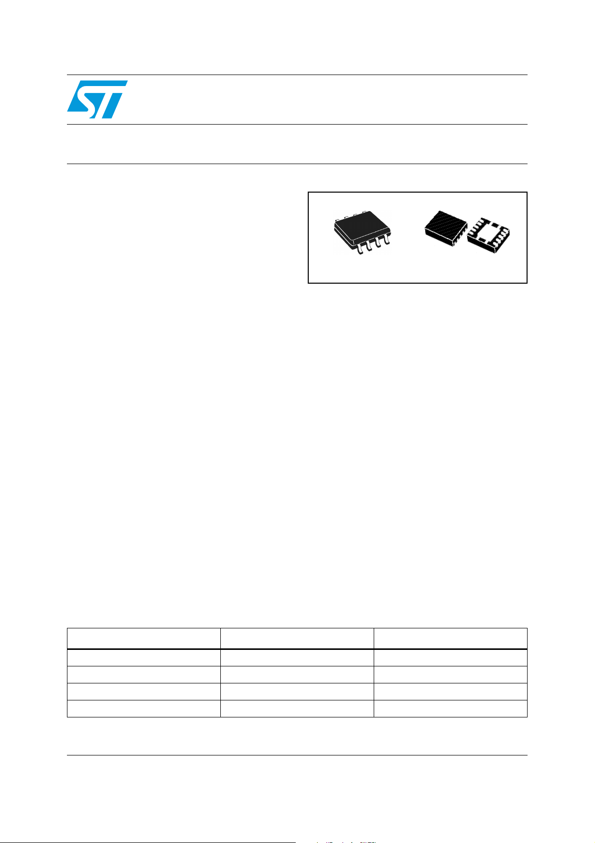
■ SO-8 and DFN10 3x3 packages
Applications
■ High current VRM / VRD for desktop / server /
workstation CPUs
■ High current and high efficiency DC / DC
converters
Description
L6743, L6743Q is a flexible, high-frequency dualdriver specifically designed to drive N-channel
MOSFETs connected in synchronous-rectified
buck topology.
L6743
L6743Q
High current MOSFET driver
SO-8
Combined with ST PWM controllers, the driver
allows implementing complete voltage regulator
solutions for modern high-current CPUs and
DCDC conversion in general. L6743, L6743Q
embeds high-current drivers for both high-side
and low-side MOSFETS. The device accepts
flexible power supply (5 V to 12 V) to optimize the
gate-drive voltage for High-Side and Low-Side
maximizing the System Efficiency.
The Bootstrap diode is embedded saving the use
of external diodes. Anti shoot-through
management avoids high-side and low-side
MOSFET to conduct simultaneously and,
combined with Adaptive Dead-Time control,
minimizes the LS body diode conduction time.
L6743, L6743Q embeds Preliminary OV
Protection: after Vcc overcomes the UVLO and
while the device is in HiZ, the LS MOSFET is
turned ON to protect the load in case the output
voltage overcomes a warning threshold protecting
the output against HS failures.
The driver is available is SO-8 and DFN10 3x3
packages
DFN10 3x3
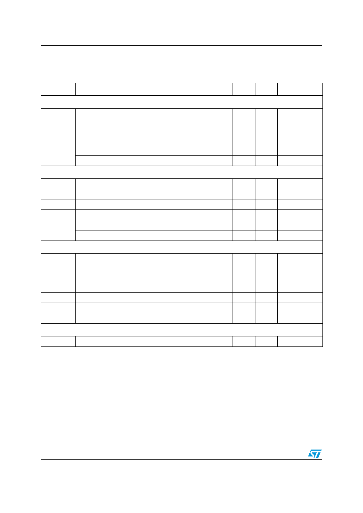
Table 1. Device summary
Order code Package Packaging
L6743 SO-8 Tube
L6743TR SO-8 Tape and reel
L6743Q DFN10 Tube
L6743QTR DFN10 Tape and reel
June 2008 Rev 2 1/17
www.st.com
1

Contents L6743, L6743Q
Contents
1 Typical application circuit and block diagram . . . . . . . . . . . . . . . . . . . . 3
1.1 Application circuit . . . . . . . . . . . . . . . . . . . . . . . . . . . . . . . . . . . . . . . . . . . . 3
1.2 Block diagram . . . . . . . . . . . . . . . . . . . . . . . . . . . . . . . . . . . . . . . . . . . . . . . 3
2 Pins description and connection diagrams . . . . . . . . . . . . . . . . . . . . . . 4
2.1 Pin description . . . . . . . . . . . . . . . . . . . . . . . . . . . . . . . . . . . . . . . . . . . . . . 4
3 Thermal data . . . . . . . . . . . . . . . . . . . . . . . . . . . . . . . . . . . . . . . . . . . . . . . 5
4 Electrical specifications . . . . . . . . . . . . . . . . . . . . . . . . . . . . . . . . . . . . . . 5
4.1 Absolute maximum ratings . . . . . . . . . . . . . . . . . . . . . . . . . . . . . . . . . . . . . 5
4.2 Electrical characteristics . . . . . . . . . . . . . . . . . . . . . . . . . . . . . . . . . . . . . . . 6
5 Device description and operation . . . . . . . . . . . . . . . . . . . . . . . . . . . . . . 7
5.1 High-impedance (HiZ) management . . . . . . . . . . . . . . . . . . . . . . . . . . . . . 8
5.2 Preliminary OV protection . . . . . . . . . . . . . . . . . . . . . . . . . . . . . . . . . . . . . 8
5.3 Internal BOOT diode . . . . . . . . . . . . . . . . . . . . . . . . . . . . . . . . . . . . . . . . . 9
5.4 Power dissipation . . . . . . . . . . . . . . . . . . . . . . . . . . . . . . . . . . . . . . . . . . . . 9
5.5 Layout guidelines . . . . . . . . . . . . . . . . . . . . . . . . . . . . . . . . . . . . . . . . . . . 11
6 Package mechanical data . . . . . . . . . . . . . . . . . . . . . . . . . . . . . . . . . . . . 13
7 Revision history . . . . . . . . . . . . . . . . . . . . . . . . . . . . . . . . . . . . . . . . . . . 16
2/17
L6743, L6743Q Typical application circuit and block diagram
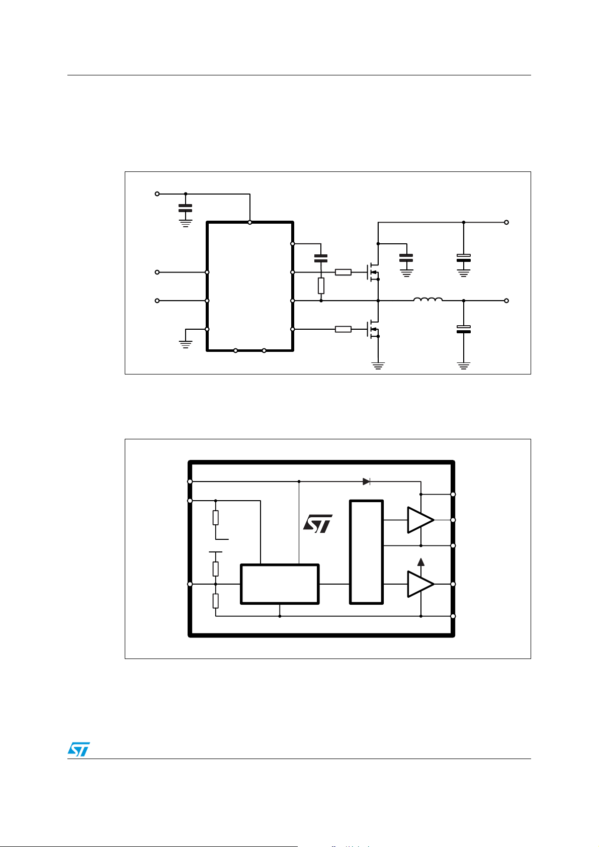
1 Typical application circuit and block diagram
1.1 Application circuit
Figure 1. Typical application circuit
VCC = 5V to 12V
C
PWM Input
DEC
PWM
VCC
BOOT
UGATE
HS
HF
C
VIN = 5V to 12V
C
BULK
EN Input
L6743 Reference Schematic
EN
GND
1.2 Block diagram
Figure 2. Block diagram
VCC
EN
PWM
15k
GND
PHASE
L6743
LGATE
NC*NC*
CONTROL LOGIC
& PROTECTIONS
L6743
PWM
LS
CROSS CONDUCTION
ADAPTIVE ANTI
HS
VCC
LS
L
Vout
C
OUT
BOOT
UGATE
PHASE
LGATE
GND
3/17
Pin description and connection diagrams L6743, L6743Q
2 Pin description and connection diagrams
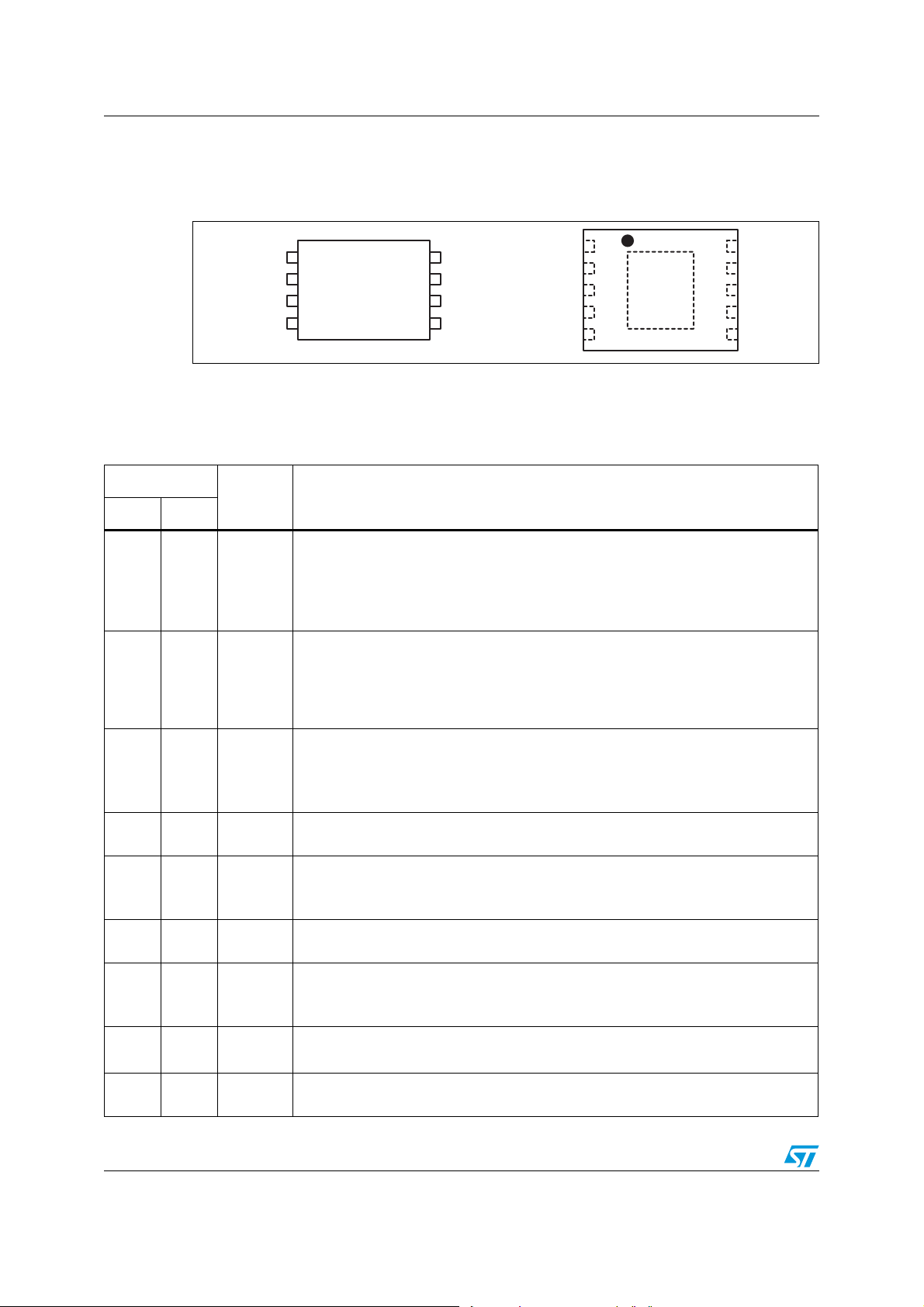
Figure 3. Pin connection (top view)
BOOT
PWM
EN
VCC
1
2
3
4
2.1 Pin description
Table 2. Pin description
Pin n
DFN10 SO-8
11BOOT
22PWM
33 EN
4, 5 4 VCC
Name Function
High-side driver supply.
This pin supplies the high-side floating driver. Connect through a R
capacitor to the PHASE pin.
Internally connected to the cathode of the integrated bootstrap diode. See
Section 5.3 for guidance in designing the capacitor value.
Control input for the driver, 5 V compatible.
This pin controls the state of the driver and which external MOSFET have to be
turned-ON according to EN status. If left floating and in conjunction with EN
asserted, it causes the driver to enter the high-impedance (HiZ) state which causes
all MOSFETs to be OFF. See Section 5.1 for details about HiZ.
Enable input for the driver. Internally pulled low by 15 kΩ.
Pull high to enable the driver according to the PWM status. If pulled low will cause
the drive to enter HiZ state with all MOSFET OFF regardless of the PWM status.
See Section 5.1 for details about HiZ.
Device and LS driver power supply. Connect to any voltage between 5 V and 12 V.
Bypass with low-ESR MLCC capacitor to GND.
L6743
8
7
6
5
UGATE
PHASE
GND
LGATE
BOOT
PWM
EN
VCC
VCC
1
2
3
L6743Q
4
56
10
9
8
7
BOOT
UGATE
PHASE
GND
GND
LGATE
- C
BOOT
Low-side driver output.
65LGATE
7, 8 6 GND
9 7 PHASE
10 8 UGATE
PA D - T H . PA D
4/17
Connect directly to the low-side MOSFET gate. A small series resistor can be useful
to reduce dissipated power especially in high frequency applications.
All internal references, logic and drivers are referenced to this pin. Connect to the
PCB ground plane.
High-side driver return path. Connect to the high-side MOSFET source.
This pin is also monitored for the adaptive dead-time management and Pre-OV
Protection.
High-side driver output.
Connect to high-side MOSFET gate.
Thermal pad connects the Silicon substrate and makes good thermal contact with
the PCB. Connect to the PGND plane. (DFN10 only)
L6743, L6743Q Thermal data
3 Thermal data
Table 3. Thermal data
Val ue
Symbol Parameter
SO8 DFN10
Unit
Thermal resistance junction to ambient
(Device soldered on 2s2p, 67 mm x 69 mm board)
Thermal resistance junction to case - 5 °C/W
Maximum junction temperature 150 °C
Storage temperature range 0 to 150 °C
Junction temperature range 0 to 125 °C
Maximum power dissipation at 25°C
(Device soldered on 2s2p PC board)
R
R
T
T
P
thJA
thJC
MAX
STG
T
J
TOT
4 Electrical specifications
4.1 Absolute maximum ratings
Table 4. Absolute maximum ratings
Symbol Parameter Value Unit
V
CC,VPVCC
V
BOOT
V
V
V
PWM, VEN
V
CC,VPVCC
, V
UGATE
PHASE
LGATE
to GND -0.3 to 15 V
to GND
to PHASE
to GND -8 to 26 V
to GND -0.3 to VCC + 0.3 V
to GND -0.3 to 7 V
to GND -0.3 to 15 V
85 45 °C/W
1.15 2.25 W
41
15
V
5/17
Electrical specifications L6743, L6743Q
4.2 Electrical characteristics
Table 5. Electrical characteristics
(V
= 12 V±15 %, TJ = 0 °C to 70 °C unless otherwise specified).
CC
Symbol Parameter Test conditions Min. Typ. Max. Unit
Supply current and power-ON
I
CC
I
BOOT
VCC supply current
BOOT supply current
VCC turn-ON VCC rising 4.1 V
UVLO
VCC
VCC turn-OFF VCC falling 3.5 V
PWM and EN input
Input high - V
PWM
Input low - V
t
HiZ
HiZ hold-off time 150 ns
Input high - V
EN
Input low - V
Input resistance to GND 15 kΩ
Gate drivers
R
HIHS
I
UGATE
R
LOHS
R
HILS
I
LGATE
R
LOLS
HS source resistance BOOT - PHASE = 12 V; 100 mA 2.3 2.8 Ω
HS source current
HS sink resistance BOOT - PHASE = 12 V; 100 mA 2 2.5 Ω
LS source resistance 100 mA 1.3 1.8 Ω
LS source current
LS sink resistance 100 mA 1 1.5 Ω
Protections
PWM_IH
PWM_IL
EN_IH
EN_IH
(1)
(1)
C
UGATE and LGATE = OPEN
BOOT = 12 V
UGATE = OPEN;
PHASE to GND; BOOT = 12 V
5mA
2mA
PWM rising 2 V
PWM falling 0.8 V
EN rising 2 V
EN falling 0.8 V
BOOT - PHASE = 12 V;
C
to PHASE = 3.3 nF
UGATE
to GND = 5.6 nF 3 A
LGATE
2A
V
PRE_OV
1. Parameter(s) guaranteed by designed, not fully tested in production
Pre-OV threshold PHASE rising 1.8 V
6/17
 Loading...