

Hybrid controller (4+1) for AMD SVID and PVID processors
Features
■ Hybrid controller: compatible with PVI and SVI
CPUs
■ Dual controller: 2 to 4 scalable phases for CPU
CORE, 1 phase for NB
■ Dual-edge asynchronous architecture with
LTB Technology
PSI management to increase efficiency in
■
light-load conditions
■ Dual over-current protection:
Average and per-phase
■ Load indicator (CORE section)
■ Logic level support for LVDDRIII
■ Voltage positioning
■ Dual remote sense
■ Adjustable independent reference offset
■ Feedback disconnection protection
■ Programmable OV protection
■ Oscillator internally fixed at 150 kHz externally
adjustable
■ LSLess startup to manage pre-biased output
■ Flexible driver support
■ HTQFP48 package
Applications
■ Hybrid high-current VRM, VRD for desktop,
server, workstation, IPC CPUs supporting PVI
and SVI interface
■ High-density DC / DC converters
tm
L6740L
HTQFP48
Description
L6740L is a hybrid CPU power supply controller
compatible with both parallel (PVI) and serial
(SVI) protocols for AMD processors.
The device embeds two independent control
loops for the CPU core and the integrated NB,
each one with its own set of protections. L6740L
is able to work in single-plane mode, addressing
only the CORE section, according to the parallel
DAC codification. When in dual-plane mode, it is
compatible with the AMD SVI specification
addressing the CPU and NB voltages according
to the SVI bus commands.
The dual-edge asynchronous architecture is optimized by LTB Technology
transient response minimizing the output capacitor and reducing the total BOM cost.
PSI management allows the device to selectively
turn-off phases when the CPU is in low-power
states increasing the over-all efficiency.
Fast protection against load over current is provided for both the sections. Furthermore,
feedback disconnection protection prevents from
damaging the load in case of disconnections in
the system board.
tm
allowing fast load-
Table 1. Device summary
Order codes Package Packaging
L6740L HTQFP48 Tube
L6740LTR HTQFP48 Tape and reel
September 2008 Rev 3 1/44
www.st.com
1

Contents L6740L
Contents
1 Typical application circuit and block diagram . . . . . . . . . . . . . . . . . . . . 4
1.1 Application circuit . . . . . . . . . . . . . . . . . . . . . . . . . . . . . . . . . . . . . . . . . . . . 4
1.2 Block diagram . . . . . . . . . . . . . . . . . . . . . . . . . . . . . . . . . . . . . . . . . . . . . . . 7
2 Pins description and connection diagrams . . . . . . . . . . . . . . . . . . . . . . 8
2.1 Pin descriptions . . . . . . . . . . . . . . . . . . . . . . . . . . . . . . . . . . . . . . . . . . . . . 8
2.2 Thermal data . . . . . . . . . . . . . . . . . . . . . . . . . . . . . . . . . . . . . . . . . . . . . . 12
3 Electrical specifications . . . . . . . . . . . . . . . . . . . . . . . . . . . . . . . . . . . . . 13
3.1 Absolute maximum ratings . . . . . . . . . . . . . . . . . . . . . . . . . . . . . . . . . . . . 13
3.2 Electrical characteristics . . . . . . . . . . . . . . . . . . . . . . . . . . . . . . . . . . . . . . 13
4 Device description and operation . . . . . . . . . . . . . . . . . . . . . . . . . . . . . 15
5 Hybrid CPU support and CPU_TYPE detection . . . . . . . . . . . . . . . . . . 16
5.1 PVI - parallel interface . . . . . . . . . . . . . . . . . . . . . . . . . . . . . . . . . . . . . . . 16
5.2 PVI start-up . . . . . . . . . . . . . . . . . . . . . . . . . . . . . . . . . . . . . . . . . . . . . . . 16
5.3 SVI - serial interface . . . . . . . . . . . . . . . . . . . . . . . . . . . . . . . . . . . . . . . . . 18
5.4 SVI start-up . . . . . . . . . . . . . . . . . . . . . . . . . . . . . . . . . . . . . . . . . . . . . . . 18
5.4.1 Set VID command . . . . . . . . . . . . . . . . . . . . . . . . . . . . . . . . . . . . . . . . . 18
5.4.2 PWROK de-assertion . . . . . . . . . . . . . . . . . . . . . . . . . . . . . . . . . . . . . . 21
5.4.3 PSI_L and efficiency optimization at light-load . . . . . . . . . . . . . . . . . . . 21
5.4.4 HiZ management . . . . . . . . . . . . . . . . . . . . . . . . . . . . . . . . . . . . . . . . . . 22
5.4.5 Hardware jumper override - V_FIX . . . . . . . . . . . . . . . . . . . . . . . . . . . . 22
6 Output voltage positioning . . . . . . . . . . . . . . . . . . . . . . . . . . . . . . . . . . . 23
6.1 CORE section - phase # programming . . . . . . . . . . . . . . . . . . . . . . . . . . 24
6.2 CORE section - current reading and current sharing loop . . . . . . . . . . . . 24
6.3 CORE section - load-line and load-indicator (optional) . . . . . . . . . . . . . . 25
6.4 CORE section - offset (optional) . . . . . . . . . . . . . . . . . . . . . . . . . . . . . . . . 26
6.5 NB section - current reading . . . . . . . . . . . . . . . . . . . . . . . . . . . . . . . . . . . 26
6.6 NB section - load-line and load-indicator (optional) . . . . . . . . . . . . . . . . . 27
6.7 NB section - offset (optional) . . . . . . . . . . . . . . . . . . . . . . . . . . . . . . . . . . 27
2/44

L6740L Contents
6.8 NB section - maximum duty-cycle limitation . . . . . . . . . . . . . . . . . . . . . . . 28
6.9 On-the-fly VID transitions . . . . . . . . . . . . . . . . . . . . . . . . . . . . . . . . . . . . . 28
6.10 Soft-start . . . . . . . . . . . . . . . . . . . . . . . . . . . . . . . . . . . . . . . . . . . . . . . . . . 30
6.10.1 LS-Less start-up . . . . . . . . . . . . . . . . . . . . . . . . . . . . . . . . . . . . . . . . . . 30
7 Output voltage monitoring and protections . . . . . . . . . . . . . . . . . . . . . 31
7.1 Programmable overvoltage . . . . . . . . . . . . . . . . . . . . . . . . . . . . . . . . . . . 31
7.2 Feedback disconnection . . . . . . . . . . . . . . . . . . . . . . . . . . . . . . . . . . . . . . 32
7.3 PWRGOOD . . . . . . . . . . . . . . . . . . . . . . . . . . . . . . . . . . . . . . . . . . . . . . . 33
7.4 Over-current . . . . . . . . . . . . . . . . . . . . . . . . . . . . . . . . . . . . . . . . . . . . . . . 33
7.4.1 CORE section . . . . . . . . . . . . . . . . . . . . . . . . . . . . . . . . . . . . . . . . . . . . 33
7.4.2 NB section . . . . . . . . . . . . . . . . . . . . . . . . . . . . . . . . . . . . . . . . . . . . . . . 34
8 Main oscillator . . . . . . . . . . . . . . . . . . . . . . . . . . . . . . . . . . . . . . . . . . . . . 36
9 System control loop compensation . . . . . . . . . . . . . . . . . . . . . . . . . . . 37
9.1 Compensation network guidelines . . . . . . . . . . . . . . . . . . . . . . . . . . . . . . 38
10 LTB Technology™ . . . . . . . . . . . . . . . . . . . . . . . . . . . . . . . . . . . . . . . . . . 39
11 Layout guidelines . . . . . . . . . . . . . . . . . . . . . . . . . . . . . . . . . . . . . . . . . . 41
11.1 Power components and connections . . . . . . . . . . . . . . . . . . . . . . . . . . . . 41
11.2 Small signal components and connections . . . . . . . . . . . . . . . . . . . . . . . 41
12 TQFP48 mechanical data and package dimensions . . . . . . . . . . . . . . 42
13 Revision history . . . . . . . . . . . . . . . . . . . . . . . . . . . . . . . . . . . . . . . . . . . 43
3/44
Typical application circuit and block diagram L6740L
1 Typical application circuit and block diagram
1.1 Application circuit
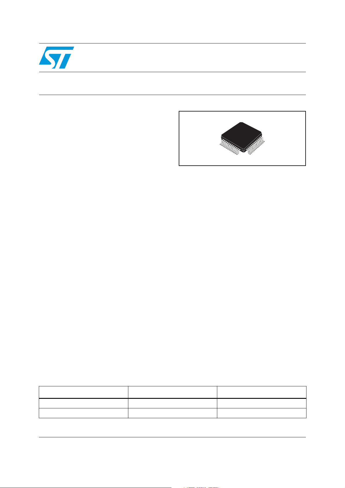
Figure 1. Typical 4+1 application circuit
PVI / SVID Bus
R
OVP
R
OSC
R
LTBG
R
C
DEC
PVCC*
VCC
PWM
EN*
GND
PWM
EN*
GND
PWM
EN*
GND
VCC
VCC
BOOT
UGATE
PHASE
L6741/3
LGATE
PVCC*
BOOT
UGATE
PHASE
L6741/3
LGATE
PVCC*
BOOT
UGATE
PHASE
L6741/3
LGATE
HS1
HS2
HS3
C
LS1
C
LS2
C
LS3
1
GND2 VCC
PWRGOOD
41
PWROK
37
EN
38
VID0
35
VID1
36
VID2/SVD
40
VID3/SVC
39
VID4
25
VID5
26
OVP / V_FIX
10
OSC / FLT
27
OS
8
NB_OS
29
LTB_GAIN
11
PSI_L
12
COMP
3
C
F
R
F
DROOP
5
FB
4
LTB
9
C
LTB
FB
34
R
LTB
NB_COMP
C
F_NBRF_NB
ST L6740L
Hybrid PVID / SVID Controller (**)
NB_DROOP
NB_FB
32
33
PWM1
PWM2
PWM3
PWM4
NB_PWM
OC_PHASE
OC_AVG / LI
CS1+
CS1-
CS2+
CS2-
CS3+
CS3-
CS4+
CS4-
NB_ISEN
FBG
VSEN
NB_VSEN
NB_FBG
ENDRV
NB_ENDRV
R
FB_NB
48
47
46
45
44
R
OC_TH
21
R
OC_AVG
28
13
14
R
G
15
16
R
G
17
18
R
G
19
20
R
G
23
R
ISEN
7
6
31
30
43
42
C
DEC
C
DEC
C
BULK_IN
HF
L1
R
C
HF
L2
R
C
HF
L3
R
V
L
IN
IN
C
DEC_NB
C
BULK_NB
C
HF_NB
HS
NB
L
NB
LS
NB
BOOT
UGATE
PHASE
LGATE
VCC
PVCC*
PWM
EN*
L6741/3
GND
PVI / SVID AM2 CPU
C
OUT_NBCMLCC_NB
(*) PVCC Only applies to L6741; EN Only applies to L6743. See related DS for further details
(**) Pin not listed to be considered as Not Connected
ST L6740L (4+1) Reference Schematic
NB
SVID / PVID Interface
4/44
CORE
C
C
DEC
VCC
PVCC*
PWM
EN*
GND
BOOT
UGATE
PHASE
L6741/3
LGATE
C
MLCC
C
OUT
HS4
HF
C
L4
LS4
R
C
L6740L Typical application circuit and block diagram
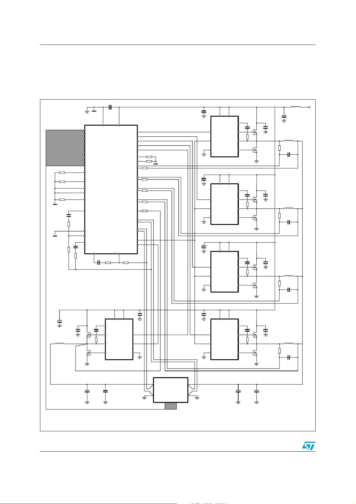
Figure 2. Typical 3+1 application circuit
PVI / SVID Bus
R
OVP
R
OSC
R
LTBG
R
C
DEC
PVCC*
VCC
PWM
EN*
GND
PWM
EN*
GND
PWM
EN*
GND
VCC
VCC
BOOT
UGATE
PHASE
L6741/3
LGATE
PVCC*
BOOT
UGATE
PHASE
L6741/3
LGATE
PVCC*
BOOT
UGATE
PHASE
L6741/3
LGATE
HS1
LS1
HS2
LS2
HS3
LS3
C
C
C
1
GND2 VCC
PWRGOOD
41
PWROK
37
EN
38
VID0
35
VID1
36
VID2/SVD
40
VID3/SVC
39
VID4
25
VID5
26
OVP / V_FIX
10
OSC / FLT
27
OS
8
NB_OS
29
LTB_GAIN
11
PSI_L
12
COMP
3
C
F
R
F
DROOP
5
FB
4
LTB
9
C
LTB
FB
34
R
LTB
NB_COMP
C
F_NBRF_NB
ST L6740L
Hybrid PVID / SVID Controller (**)
NB_DROOP
NB_FB
32
33
PWM1
PWM2
PWM3
PWM4
NB_PWM
OC_PHASE
OC_AVG / LI
CS1+
CS1-
CS2+
CS2-
CS3+
CS3-
CS4+
CS4-
NB_ISEN
FBG
VSEN
NB_VSEN
NB_FBG
ENDRV
NB_ENDRV
R
FB_NB
48
47
46
45
44
21
R
OC_TH
28
R
OC_AVG
13
14
R
G
15
16
R
G
17
18
R
G
19
20
R
G
23
R
ISEN
7
6
31
C
DEC
30
43
42
C
DEC
C
BULK_IN
HF
L1
R
C
HF
L2
R
C
HF
L3
R
V
L
IN
IN
C
DEC_NB
C
BULK_NB
C
HF_NB
HS
NB
L
NB
LS
NB
C
OUT_NBCMLCC_NB
(*) PVCC Only applies to L6741; EN Only applies to L6743. See related DS for further details
(**) Pin not listed to be considered as Not Connected
BOOT
UGATE
PHASE
LGATE
VCC
PVCC*
PWM
EN*
L6741/3
GND
ST L6740L (3+1) Reference Schematic
PVI / SVID AM2 CPU
NB
SVID / PVID Interface
CORE
C
C
MLCC
C
OUT
5/44
Typical application circuit and block diagram L6740L
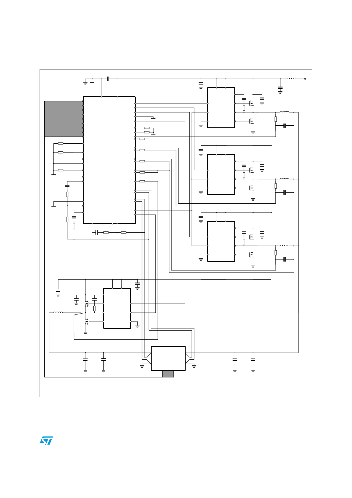
Figure 3. Typical 2+1 application circuit
PVI / SVID Bus
R
OVP
R
OSC
R
LTBG
R
C
DEC
PVCC*
VCC
PWM
EN*
GND
PWM
EN*
GND
VCC
BOOT
UGATE
PHASE
L6741/3
LGATE
PVCC*
BOOT
UGATE
PHASE
L6741/3
LGATE
HS1
LS1
HS2
LS2
C
C
1
GND2 VCC
PWRGOOD
41
PWROK
37
EN
38
VID0
35
VID1
36
VID2/SVD
40
VID3/SVC
39
VID4
25
VID5
26
OVP / V_FIX
10
OSC / FLT
27
OS
8
NB_OS
29
LTB_GAIN
11
PSI_L
12
COMP
3
C
F
R
F
DROOP
5
FB
4
LTB
9
C
LTB
FB
NB_COMP
34
R
LTB
C
F_NBRF_NB
OC_AVG / LI
ST L6740L
Hybrid PVID / SVID Controller (**)
NB_ENDRV
NB_DROOP
NB_FB
32
33
PWM1
PWM2
PWM3
PWM4
NB_PWM
OC_PHASE
CS1+
CS1-
CS2+
CS2-
CS3+
CS3-
CS4+
CS4-
NB_ISEN
FBG
VSEN
NB_VSEN
NB_FBG
ENDRV
R
FB_NB
48
47
46
45
44
21
R
OC_TH
R
OC_AVG
28
13
14
R
G
15
16
R
G
17
18
R
G
19
20
R
G
23
R
ISEN
7
6
31
C
DEC
30
43
42
C
BULK_IN
HF
L1
R
C
HF
L2
R
C
V
L
IN
IN
C
DEC_NB
C
BULK_NB
C
HF_NB
HS
NB
L
NB
LS
NB
BOOT
UGATE
PHASE
LGATE
VCC
PVCC*
PWM
EN*
L6741/3
GND
PVI / SVID AM2 CPU
C
OUT_NBCMLCC_NB
(*) PVCC Only applies to L6741; EN Only applies to L6743. See related DS for further details
(**) Pin not listed to be considered as Not Connected
NB
SVID / PVID Interface
ST L6740L (2+1) Reference Schematic
6/44
CORE
C
MLCC
C
OUT
L6740L Typical application circuit and block diagram
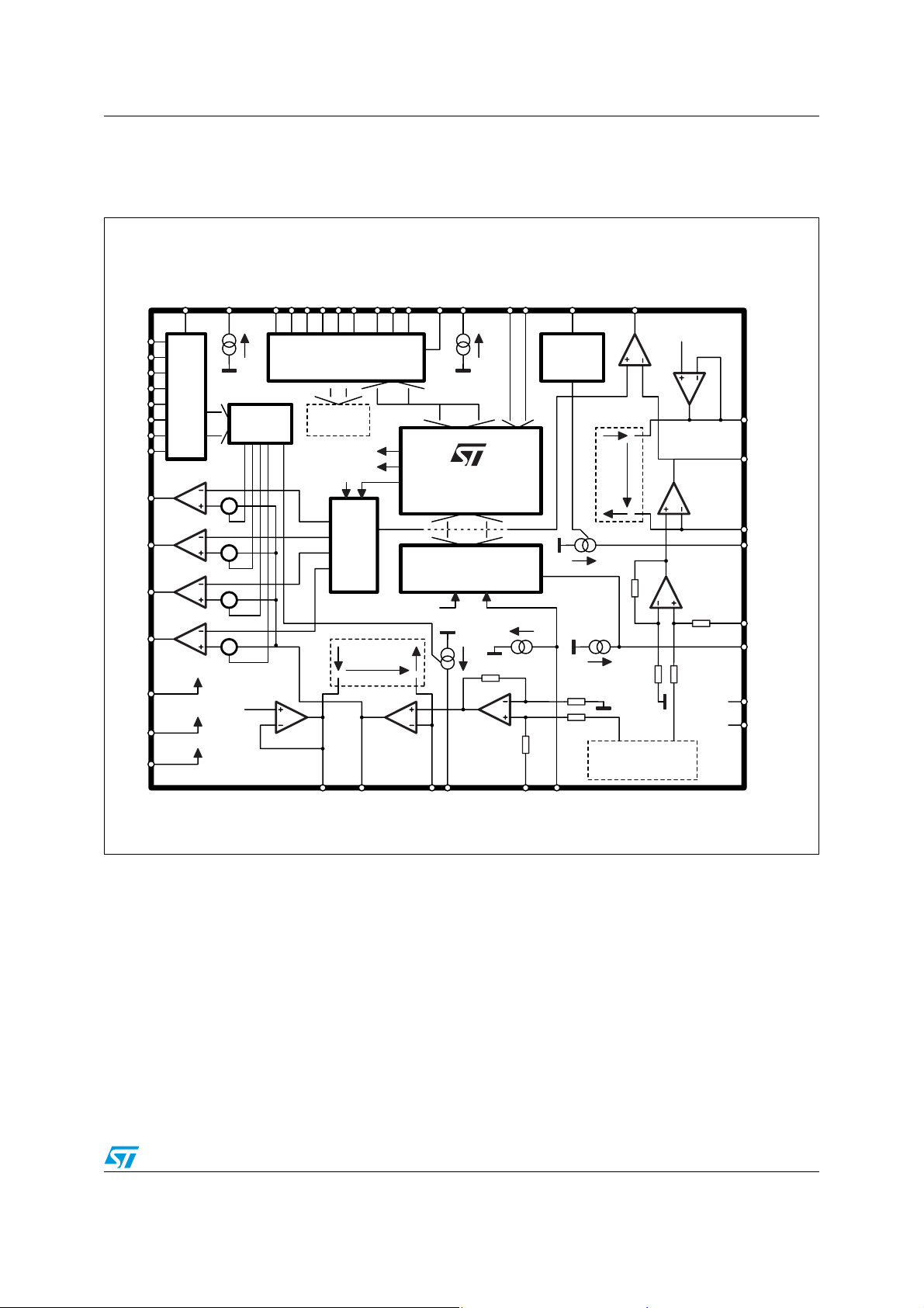
1.2 Block diagram
Figure 4. Block diagram
VID4
V_FIX / OVP
OC_PHASE
VID0
VID2 / SVD
VID1
VID5ENPWROK
VID3 / SVC
PWRGOOD
PSI_L
OC_AVG / LI
LT B
LTB_GAIN
NB_ISEN
NB_PWM
CS1+
CS1-
CS2+
CS2-
CS3+
CS3-
CS4+
CS4-
PWM1
PWM2
PWM3
PWM4
OSC
VCC
SGND
PWM1
PWM2
PWM3
PWM4
DIFFERENTIAL
CURRENT SENSE
Σ
Σ
Σ
Σ
OSC
VCC
SGND
AMD SVI / PVI FLEXIBLE
11 μA
CURRENT
BALANCE
1.24V
OFFSET
INTERFACE
CORE_REF
& NB_REF
ENDRV
NB_ENDRV
OSC
DUAL CHANNEL
OSCILLATOR (4+1)
CORE - TOT CURRENT
I
OS
ERROR
AMPLIFIER
DROOP
I
L6740L
CONTROL LOGIC
OUTPUT VOLTAGE
MONITOR AND PROTECTION
MANAGEMENT
CS1-
I
I
OS
DROOP
64k
BUFFER
30μA
I
64k
NB CURR
SENSE
NB_DROOP
50μA +I
NB_OS
I
NB - TOT CURRENT
NB_OS
I
NB_OS
64k
64kREMOTE
VCORE_REF
(from SVI/PVI decoding)
NB_PWM
64k64k
NB_REF
1.24V
ERROR
AMPLIFIER
BUFFER
REMOTE
64k
64k
ENDRV
NB_ENDRV
OFFSET
NB_OS
NB_COMP
NB_FB
NB_DROOP
NB_FBG
NB_VSEN
ENDRV
NB_ENDRV
OS
COMP
FB
DROOP
FBG
VSEN
7/44
Pins description and connection diagrams L6740L
2 Pins description and connection diagrams
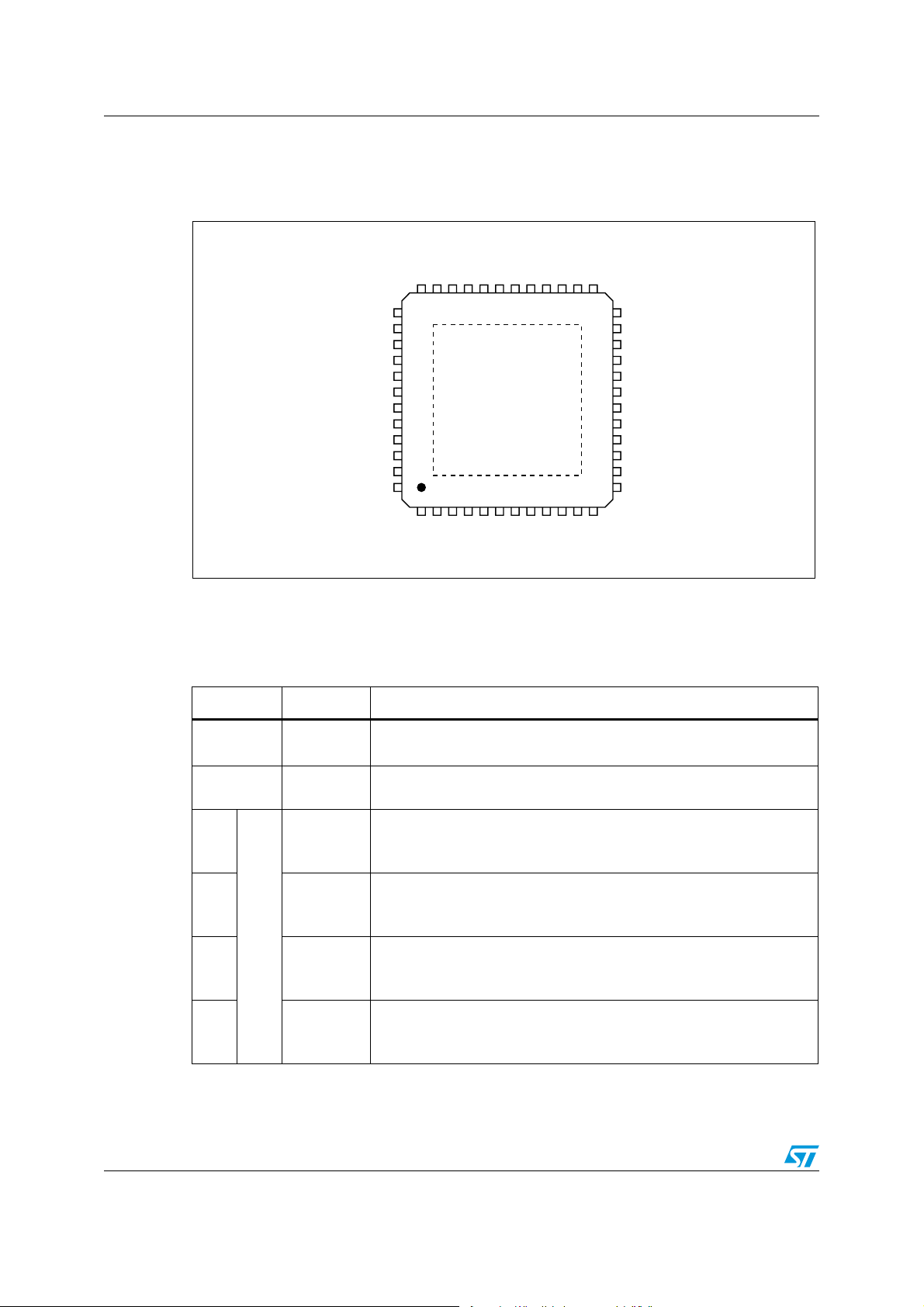
Figure 5. Pins connection (top view)
VID1
VID0
NB_COMP
NB_FB
NB_DROOP
NB_VSEN
NB_FBG
NB_OS
OC_AVG / LI
OSC / FLT
VID5
VID4
36 35 34 33 32 31 30 29 28 27 26 25
PWROK
EN
SVC
SVD
PWRGOOD
NB_ENDRV
ENDRV
NB_PWM
PWM4
PWM3
PWM2
PWM1
37
38
39
40
41
42
43
44
45
46
47
48
123456789101112
L6740L
24
23
22
21
20
19
18
17
16
15
14
13
N.C.
NB_ISEN
N.C.
OC_PHASE
CS4-
CS4+
CS3-
CS3+
CS2-
CS2+
CS1-
CS1+
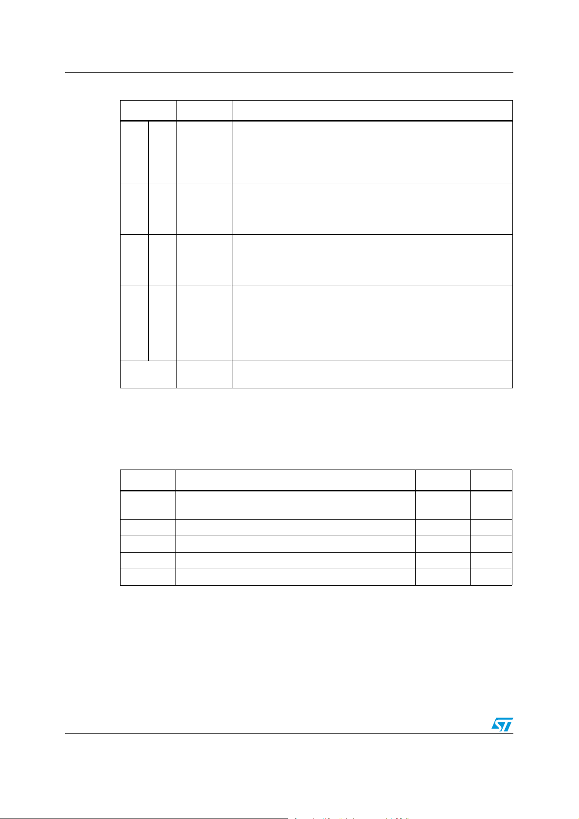
2.1 Pin descriptions
Table 2. Pin description
Pin# Name Function
1VCC
2SGND
3
4FB
5DROOP
COMP
Core section
VCC
GND
COMP
FB
DROOP
VSEN
FBG
OS
LTB
LTB_GAIN
OVP/V_FIX
PSI_L
Device power supply.
Operative voltage is 12V ±15%. Filter with 1μF MLCC to SGND.
All the internal references are referred to this pin. Connect to the PCB
signal ground.
Error amplifier output.
Connect with an R
- CF to FB. The CORE section or the device cannot
F
be disabled by grounding this pin.
Error amplifier inverting input.
Connect with a resistor R
to VSEN and with an RF - CF to COMP.
FB
Offset current programmed by OS is sunk through this pin.
A current proportional to the total current read is sourced from this pin
according to the current reading gain.
Short to FB to implement droop function, if not used, short to SGND.
Output voltage monitor.
6 VSEN
It manages OVP and UVP protections and PWRGOOD. Connect to the
positive side of the load for remote sensing. See Section 7 for details.
8/44

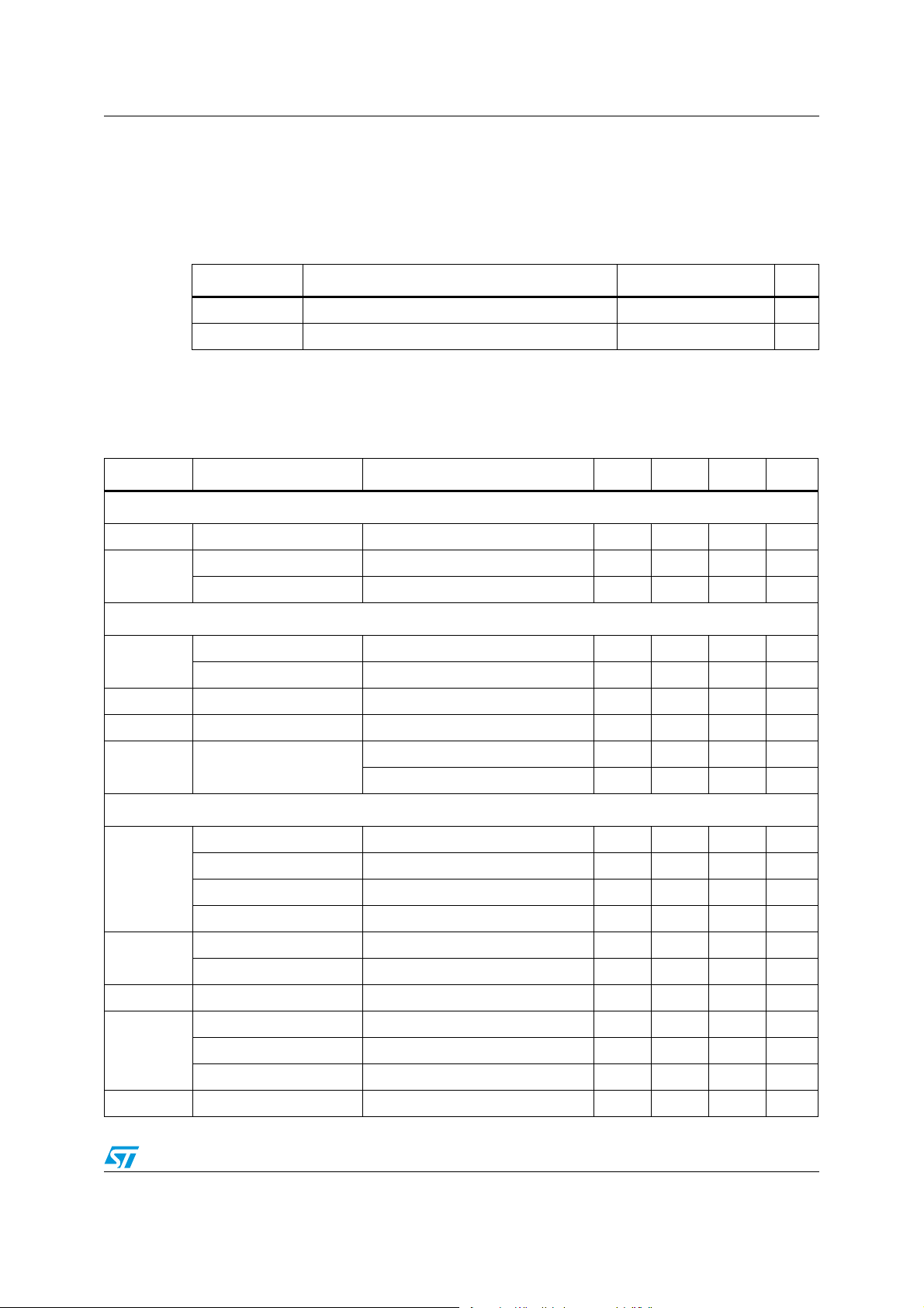
L6740L Pins description and connection diagrams
Table 2. Pin description (continued)
Pin# Name Function
Remote ground sense.
7
8OS
Core section
9LTB
10 OVP / V_FIX
11
Core
12 PSI_L
13
LT B_ GA IN
section
FBG
CS1+
Connect to the negative side of the load for remote sensing. See
Section 9 for proper layout of this connection.
Offset programming pin.
Internally set to 1.24 V. Connecting a R
resistor to SGND allows to
OS
set a current that is mirrored into FB pin in order to program a positive
offset according to the selected R
FB
.
Short to SGND to disable the function. See Section 6.4 for details.
TM
LTB Te c h n o lo g y
Connect through an R
input pin.
- C
LT B
network to the regulated voltage
LT B
(CORE section) to detect load transient. See Section 10 for details.
OVP. Overvoltage programming pin. Internally pulled-up to 3.3 V by
11 μA. Connect to SGND through a R
(typ) to set a fixed voltage according to the R
resistor and filter with 10 nF
OVP
resistor. If floating it
OVP
will program 3.3 V threshold. See Section 7 for details.
V_FIX - Hardware override. Short to SGND to enter VFIX mode
(WARNING: this condition overrides any code programmed on the VIDx
lines). In this case, the device will use SVI inputs as static VIDs and
OVP threshold will be set to 1.8 V. See Section 5.4.5 for details.
TM
LTB Te c h n o lo g y
Connect to SGND through a resistor R
gain pin.
to program the LTB
LTBGAIN
Gain. See Section 10 for details.
Power saving indicator (SVI mode).
Open-drain input/output pin. See Section 5.4.3 for details.
Channel 1 current sense positive Input. Connect through an R-C filter to
the phase-side of the channel 1 inductor.
See Section 9 for proper layout of this connection.
14 CS1-
15 CS2+
16 CS2-
Core section
17 CS3+
18 CS3-
Channel 1 current sense negative input. Connect through a R
resistor
G
to the output-side of the channel inductor.
See Section 9 for proper layout of this connection.
Channel 2 current sense positive input. Connect through an R-C filter to
the phase-side of the channel 2 inductor.
See Section 9 for proper layout of this connection.
Channel 2 current sense negative input. Connect through a R
resistor
G
to the output-side of the channel inductor.
See Section 9 for proper layout of this connection.
Channel 3 current sense positive input. Connect through an R-C filter to
the phase-side of the channel 3 inductor. When working at 2 phase,
directly connect to V
out_CORE
.
See Section 9 for proper layout of this connection.
Channel 3 current sense negative input. Connect through a R
resistor
G
to the output-side of the channel inductor. When working at 2 phase,
connect through R
to CS3+.
G
See Section 9 for proper layout of this connection.
9/44
Pins description and connection diagrams L6740L
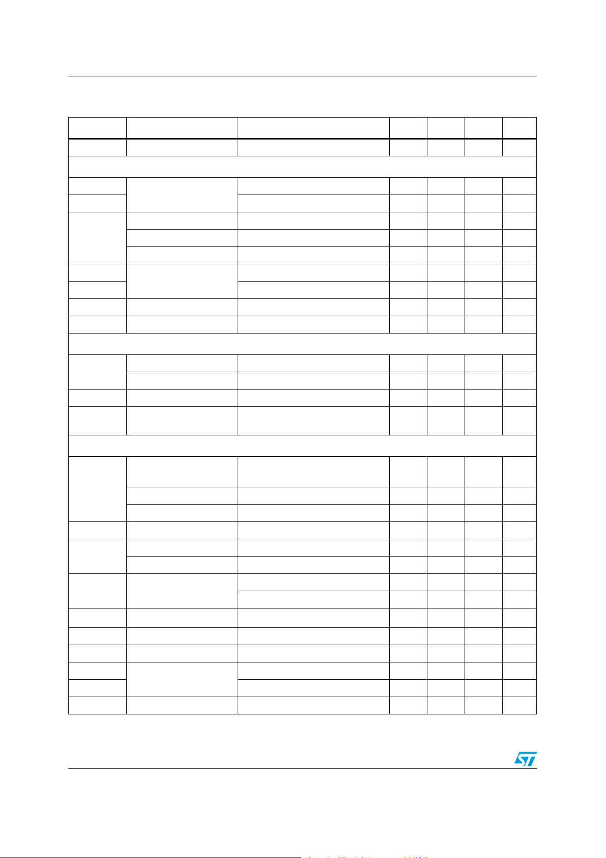
Table 2. Pin description (continued)
Pin# Name Function
Channel 4 current sense positive input. Connect through an R-C filter to
19
CS4+
20 CS4-
Core section
21 OC_PHASE
22 NC Not internally connected.
NB
NB_ISEN
section
23
24 NC Not internally connected.
25,
26
PVI
VID4, VID5
interface
27 OSC / FLT
28
OC_AVG /
LI
Core section
29
NB_OS
NB section
30 NB_FBG
the phase-side of the channel 4 inductor. When working at 2 or 3
phase, directly connect to V
out_CORE
.
See Section 9 for proper layout of this connection.
Channel 4 current sense negative input. Connect through a R
resistor
G
to the output-side of the channel inductor. When working at 2 or 3
phase, connect through R
to CS4+.
G
See Section 9 for proper layout of this connection.
Per-phase over-current (CORE section).
Internally set to 1.24 V, connecting to SGND with a resistor R
OC_TH
it
programs the OC threshold per-phase. See Section 7.4.1 for details.
NB current sense pin.
Used for NB voltage positioning and NB_OCP. Connect through a
resistor R
to the relative LS Drain. See Section 7.4 for details.
ISEN
Voltage IDentification pins.
Internally pulled-low by 10 μA, they are used to program the output
voltage. Used only in PVI-mode, ignored when in SVI-mode.
See Section 5 for details.
OSC: It allows programming the switching frequency F
of both
SW
sections. Switching frequency can be increased according to the
resistor R
connected from the pin to. SGND with a gain of
OSC
6.8 kHz/µA (see Section 8 for details). If floating, the switching
frequency is 150 kHz per phase.
FLT: The pin is forced high (3.3 V) in case of an OV / UV fault. To
recover from this condition, cycle VCC or the EN pin. See Section 7 for
details.
Average over-current and load indicator pin.
A current proportional to the current delivered by the CORE section (a
copy of the DROOP current) is sourced through this pin.
The average-OC threshold is programmed by connecting a resistor
R
threshold (V
to SGND. When the generated voltage crosses the OC_AVG
OC_AVG
OC_AVGTH
= 2.5 V Typ) the device latches with all mosfets
OFF (to recover, cycle VCC or the EN pin).
A load indicator with 2.5 V end-of-scale is then implemented.
See Section 7.4.1 for details.
Offset programming pin.
Internally set to 1.24 V, connecting a R
resistor to SGND allows
OS_NB
setting a current that is mirrored into NB_FB pin in order to program a
positive offset according to the selected R
. Short to SGND to
FB_NB
disable the function. See Section 6.7 for details.
Remote ground sense.
Connect to the negative side of the load to perform remote sense. See
Section 9 for proper layout of this connection.
10/44
L6740L Pins description and connection diagrams
Table 2. Pin description (continued)
Pin# Name Function
NB output voltage monitor.
31
NB_VSEN
32 NB_DROOP
It manages OVP and UVP protections and PWRGOOD. Connect to the
positive side of the NB load to perform remote sensing. See Section 9
for proper layout of this connection.
A current proportional to the total current read by the NB section is
sourced through this pin according to the current reading gain (R
ISEN
).
Short to NB_FB to implement Droop Function or connect to SGND
through a resistor and filter with 1nF capacitor to implement NB LOAD
Indicator. If not used, short to SGND.
NB section
33 NB_FB
34 NB_COMP
35,
36
37 PWROK
VID0, VID1
SVI / PVI interface
38 EN
39
SVC / VID3
NB error amplifier inverting input.
Connect with a resistor R
to NB_VSEN and with an R
FB_NB
F_NB
- C
F_NB
to NB_COMP. Offset current programmed by NB_OS is sunk through
this pin.
Error amplifier output.
Connect with an R
F_NB
- C
to NB_FB. The NB section or the device
F_NB
cannot be disabled by grounding this pin.
Voltage IDentification pins.
Internally pulled-low by 10 μA, they are used to program the output
voltage. VID1 is monitored on the EN pin rising-edge to define the
operative mode of the controller (SVI or PVI). When in SVI mode, VID0
is ignored. See Section 5 for details.
System-wide Power Good input (SVI mode).
Internally pulled-low by 10 μA. When low, the device will decode the two
SVI bits (SVC, SVD) to determine the Pre-PWROK Metal VID (default
condition when pin is floating).
When high, the device will actively run the SVI protocol.
Pre-PWROK Metal VID are latched after EN is asserted and re-used in
case of PWROK de-assertion. Latch is reset by VCC or EN cycle.
VR Enable. Internally pulled-up to 3.3 V by 10 μA.
Pull-low to disable the device. When set free, the device immediately
checks for the VID1 status to determine the SVI / PVI protocol to be
adopted and configures itself accordingly. See Section 5 for details.
Voltage IDentification pin - SVI clock pin.
Internally pulled-low by 10 μA, it is used to program the output voltage.
When in SVI-mode, it is considered as Serial-VID-data (input / open
drain output). See Section 5 for details.
40 SVD / VID2
SVI / PVI interface
41 PWRGOOD
Voltage IDentification pins - SVI data pin.
Internally pulled-low by 10 μA, it is used to program the output voltage.
When in SVI-mode, it is considered as Serial-VID-data (input / open
drain output). See Section 5 for details.
VCORE and NB Power Good.
It is an open-drain output set free after SS as long as both the voltage
planes are within specifications. Pull-up to 3.3V (typ) or lower, if not
used it can be left floating.
When in PVI mode, it monitors the CORE section only.
11/44
Pins description and connection diagrams L6740L
Table 2. Pin description (continued)
Pin# Name Function
External driver enable.
Open drain output used to control NB section external driver status:
42
43
44
45 to
48
NB
section
CORE
section
NB
section
CORE
section
Thermal pad
NB_ENDRV
ENDRV
NB_PWM
PWM1 to
PWM4
pulled-low to manage HiZ conditions or pulled-high to enable the driver.
Pull up to 3.3 V (typ) or lower.
When in PVI mode, NB section is always kept in HiZ.
External driver enable.
Open drain output used to control CORE section external driver status:
pulled-low to manage HiZ conditions or pulled-high to enable the driver.
Pull up to 3.3 V (typ) or lower.
PWM output.
Connect to external driver PWM input. The device is able to manage
HiZ status by setting the pin floating. When in PVI mode, NB section is
kept in HiZ. See Section 5.4.4 for details about HiZ management.
PWM outputs.
Connect to external drivers PWM inputs. The device is able to manage
HiZ status by setting the pins floating.
By shorting to SGND PWM4 or PWM3 and PWM4, it is possible to
program the CORE section to work at 3 or 2 phase respectively.
See Section 5.4.4 for details about HiZ management.
Thermal pad connects the silicon substrate and makes good thermal
contact with the PCB. Connect to the PGND plane.
2.2 Thermal data
Table 3. Thermal data
Symbol Parameter Value Unit
R
R
T
T
thJA
thJC
MAX
STG
T
J
Thermal resistance junction to ambient
(device soldered on 2s2p PC board)
Thermal resistance junction to case 1 °C/W
Maximum junction temperature 150 °C
Storage temperature range -40 to 150 °C
Junction temperature range 0 to 125 °C
40 °C/W
12/44
L6740L Electrical specifications
3 Electrical specifications
3.1 Absolute maximum ratings
Table 4. Absolute maximum ratings
Symbol Parameter Value Unit
V
CC
to PGND 15 V
All other pins to PGNDx -0.3 to 3.6 V
3.2 Electrical characteristics
Table 5. Electrical characteristics
(V
= 12 V ± 15%, TJ = 0 °C to 70 °C unless otherwise specified).
CC
Symbol Parameter Test conditions Min. Typ. Max. Unit
Supply current and power-ON
I
CC
UVLO
Oscillator
F
SW
ΔV
OSC
FAULT Voltage at pin OSC OVP, UVP latch active 3 3.6 V
d
MAX_NB
PVI / SVI interface
VCC supply current 20 mA
VCC turn-ON VCC rising 9 V
VCC
VCC turn-OFF VCC falling 7 V
Main oscillator accuracy 135 150 165 kHz
Oscillator adjustability R
PWM ramp amplitude CORE and NB section 2 V
NB duty-cycle limit
= 27 kΩ 380 465 550 kHz
OSC
I
NB_DROOP
I
NB_DROOP
= 0 μA80%
= 35 μA40%
Input high 2 V
EN,
PWROK
VID2,/SVD
VID3/SVC
SVD Voltage low (ACK) I
VID0 to
VID5
V_FIX Entering V_FIX mode 0.90 V
Input low 0.80 V
Pull-up current EN pin 10 μA
Pull-down current PWORK pin 10 μA
Input high (SVI mode) 0.95 V
Input low (SVI mode) 0.65 V
= -5 mA 250 mV
SINK
Input high (PVI mode) 1.3 V
Input low (PVI mode) 0.80 V
Pull-down current 10 μA
13/44
Electrical specifications L6740L
Table 5. Electrical characteristics (continued)
(V
= 12 V ± 15%, TJ = 0 °C to 70 °C unless otherwise specified).
CC
Symbol Parameter Test conditions Min. Typ. Max. Unit
PSI_L Voltage low I
= -5 mA 250 mV
SINK
Voltage positioning (CORE and NB section)
CORE
Output voltage accuracy
NB NBVSEN to V
OFFSET bias voltage I
OS, NB_OS
OFFSET current range 0 250 μA
VSEN to V
= 0 to 250 μA 1.190 1.24 1.290 V
OS
; FBG to GND
CORE
; NBFBG to GND
NB
CORE
-8 8 mV
-10 10 mV
FB
OFFSET - IFB accuracy IOS = 0 to 250 μA -15 15 %
DROOP
DROOP accuracy
NB_DROOP I
A
0
EA DC gain 100 dB
= 0 to 140 μA; OS = OFF -9 9 μA
I
DROOP
NB_DROOP
= 0 to 35 μA; OS = OFF -4 4 μA
SR Slew rate COMP, NB_COMP to SGND = 10pF 20 V/μs
PWM outputs (CORE and NB section)
PWMx,
NB_PWM
I
PWMx
ENDRV,
NB_ENDRV
Output high I = 1 mA 3 3.6 V
Output low I = -1 mA 0.2 V
Test current 10 μA
Output low I = -5 mA 0.4 V
Protections
V_FIX mode (V_FIX = SGND);
VSEN, NB_VSEN rising
= 180 kΩ 1.730 1.800 1.870 V
OVP
1.720 1.800 1.880 V
OVP
Overvoltage protection
Bias current 7 11 15 μA
OV programmability R
UVP Under voltage protection VSEN, NB_VSEN falling; wrt Ref. -470 -400 -330 mV
PGOOD threshold VSEN, NB_VSEN falling; wrt Ref -300 -250 -200 mV
PWRGOOD
Voltage low I
PWRGOOD
= -4 mA 0.4 V
Sourced from NB_VSEN; OS = OFF 50 μA
I
VSEN-DISC
V
FB-DISC
VSEN disconnection
FB disconnection
Sunk from VSEN; OS = OFF 30 μA
CORE - V
rising, above VSEN
CS-
500 600 700 mV
FBG DISC FBG disconnection EA NI input wrt VID 350 450 550 mV
OC_PHASE Per-phase OC CORE section; bias voltage 1.200 1.240 1.280 V
kV
OC_AVGTH
kI
OC_AVGTH
I
OCTH_NB
Average OC
OC threshold NB section 32 37.5 43 μA
CORE section 2.430 2.500 2.570 V
I
= 0 to 140 μA; OS = OFF -11 11 μA
DROOP
14/44

L6740L Device description and operation
4 Device description and operation
L6740L is a hybrid CPU power supply controller compatible with both parallel (PVI) and
Serial (SVI) protocols for AMD K8 - second generation processors. The device provides
complete control logic and protections for a high-performance step-down DC-DC voltage
regulator, optimized for advanced microprocessor power supply supporting both PVI and
SVI communication. It embeds two independent controllers for CPU CORE and the
integrated NB, each one with its own set of protections.
L6740L is able to detect which kind of CPU is connected in order to configure itself to work
as a single-plane PVI controller or dual-plane SVI controller.
The controller performs a single-phase control for the NB section and a programmable 2-to4 phase control for the CORE section featuring dual-edge non-latched architecture: this
allows fast load-transient response optimizing the output filter consequently reducing the
total BOM cost. Further reduction can be achieved by enabling LTB Technology
phase (when enabled) will be automatically phase-shifted with respect to the CORE phases
in order to reduce the total input RMS current amount.
PSI_L Flag is sent to the VR through the SVI bus. The controller monitors this flag and
selectively modifies the phase number in order to optimize the system efficiency when the
CPU enters low-power states. This causes the over-all efficiency to be maximized at light
loads so reducing losses and system power consumption.
(TM)
. NB
Both sections feature programmable over-voltage protection and adjustable constant overcurrent protection. Voltage positioning (LL) is possible thanks to an accurate fully-differential
current-sense across the main inductors for the CORE section and thanks to the loss-less
current sense across low-side MOSFET R
be disabled and the generated current information may be used to implement a Load
Indicator function.
L6740L features dual remote sensing for the regulated outputs (CORE and NB) in order to
recover from PCB voltage drops also protecting the load from possible feedback network
disconnections.
LSLess start-up function allows the controller to manage pre-biased start-up avoiding
dangerous current return through the main inductors as well as negative undershoot on the
output voltage if the output filter is still charged before start-up.
L6740L also supports V_FIX mode for system debugging: in this particular configuration the
SVI bus is used as a static bus configuring 4 operative voltages for both the sections and
ignoring any serial-VID command.
When working in PVI mode, the device features on-the-fly VID management: VID code is
continuously sampled and the reference update according to the variation detected,
L6740L is available in TQFP48 package.
for the NB section. In both cases, LL may
DS(on)
15/44

Hybrid CPU support and CPU_TYPE detection L6740L
5 Hybrid CPU support and CPU_TYPE detection
L6740L is able to detect the type of the CPU-core connected and to configure itself
accordingly. At system start-up, on the rising-edge of the EN signal, the device monitors the
status of VID1 and configures the PVI mode (VID1 = 1) or SVI mode (VID1 = 0).
When in PVI mode, L6740L uses the information available on the VID[0: 5] bus to address
the CORE section output voltage according to
When in SVI mode, L6740L ignores the information available on VID0, VID4 and VID5 and
uses VID2 and VID3 as a SVI bus addressing the CORE and NB sections according to the
SVI protocol.
Caution: To avoid any risk of errors in CPU type detection (i.e. detecting SVI CPU when PVI CPU is
installed on the socket and vice versa), it is recommended to carefully control the start-up
sequencing of the system hosting L6740L in order to ensure than on the EN rising-edge,
VID1 is in valid and correct state.
5.1 PVI - parallel interface
PVI is a 6-bit-wide parallel interface used to address the CORE section reference. According
to the selected code, the device sets the CORE section reference and regulates its output
voltage as reported into
Ta bl e 6 .
Ta bl e 6. NB section is kept in HiZ mode.
NB section is always kept in HiZ; no activity is performed on this section. Furthermore,
PWROK information is ignored as well since the signal only applies to the SVI protocol.
5.2 PVI start-up
Once the PVI mode has been detected, the device uses the whole code available on the
VID[0:5] lines to define the reference for the CORE section. NB section is kept in HiZ.
Soft-start to the programmed reference is performed regardless of the state of PWROK.
See Section 6.10 for details about soft-start.
Figure 6. System start-up: SVI (to metal-VID; left) and PVI (right)
16/44

L6740L Hybrid CPU support and CPU_TYPE detection
Table 6. Voltage identifications (VID) codes for PVI mode
VID5 VID4 VID3 VID2 VID1 VID0
0000001.5500 1 0 0 0 0 0 0.7625
0000011.5250 1 0 0 0 0 1 0.7500
0000101.5000 1 0 0 0 1 0 0.7375
0000111.4750 1 0 0 0 1 1 0.7250
0001001.4500 1 0 0 1 0 0 0.7125
0001011.4250 1 0 0 1 0 1 0.7000
0001101.4000 1 0 0 1 1 0 0.6875
0001111.3750 1 0 0 1 1 1 0.6750
0010001.3500 1 0 1 0 0 0 0.6625
0010011.3250 1 0 1 0 0 1 0.6500
0010101.3000 1 0 1 0 1 0 0.6375
0010111.2750 1 0 1 0 1 1 0.6250
0011001.2500 1 0 1 1 0 0 0.6125
Output
voltage
VID5 VID4 VID3 VID2 VID1 VID0
Output
voltage
0011011.2250 1 0 1 1 0 1 0.6000
0011101.2000 1 0 1 1 1 0 0.5875
0011111.1750 1 0 1 1 1 1 0.5750
0100001.1500 1 1 0 0 0 0 0.5625
0100011.1250 1 1 0 0 0 1 0.5500
0100101.1000 1 1 0 0 1 0 0.5375
0100111.0750 1 1 0 0 1 1 0.5250
0101001.0500 1 1 0 1 0 0 0.5125
0101011.0250 1 1 0 1 0 1 0.5000
0101101.0000 1 1 0 1 1 0 0.4875
0101110.9750 1 1 0 1 1 1 0.4750
0110000.9500 1 1 1 0 0 0 0.4625
0110010.9250 1 1 1 0 0 1 0.4500
0110100.9000 1 1 1 0 1 0 0.4375
0110110.8750 1 1 1 0 1 1 0.4250
0111000.8500 1 1 1 1 0 0 0.4125
0111010.8250 1 1 1 1 0 1 0.4000
0111100.8000 1 1 1 1 1 0 0.3875
0111110.7750 1 1 1 1 1 1 0.3750
17/44

Hybrid CPU support and CPU_TYPE detection L6740L
5.3 SVI - serial interface
SVI is a two wire, clock and data, bus that connects a single master (CPU) to one slave
(L6740L). The master initiates and terminates SVI transactions and drives the clock, SVC,
and the data, SVD, during a transaction. The slave receives the SVI transactions and acts
accordingly. SVI wire protocol is based on fast-mode I
SVI interface also considers two additional signal needed to manage the system start-up.
These signals are EN and PWROK. The device return a PWRGOOD signal if the output
voltages are in regulation.
2
C.
5.4 SVI start-up
Once the SVI mode has been detected on the EN rising-edge, L6740L checks for the status
of the two serial VID pins, SVC and SVD, and stores this value as the Pre-PWROK Metal
VID. The controller initiate a soft-start phase regulating both CORE and NB voltage planes
to the voltage level prescribed by the Pre-PWROK Metal VID. See Tab le 7 for details about
Pre-PWROK Metal VID codifications. The stored Pre-PWROK Metal VID value are re-used
in any case of PWROK de-assertion.
After bringing the output rails into regulation, the controller asserts the PWRGOOD signal
and waits for PWROK to be asserted. Until PWROK is asserted, the Controller regulates to
the Pre-PWROK Metal VID ignoring any commands coming from the SVI interface.
After PWROK is asserted, the processor has initialized the serial VID interface and L6740L
waits for commands from the CPU to move the voltage planes from the Pre-PWROK Metal
VID values to the operative VID values. As long as PWROK remains asserted, the controller
will react to any command issued through the SVI interface according to SVI Protocol.
See Section 6.10 for details about soft-start.
Table 7. V_FIX mode and metalVID
SVC SVD
0 0 1.1V 1.4V
0 1 1.0V 1.2V
1 0 0.9V 1.0V
1 1 0.8V 0.8V
5.4.1 Set VID command
The Set VID Command is defined as the command sequence that the CPU issues on the
SVI bus to modify the voltage level of the CORE section and/or the NB section.
During a Set VID Command, the processor sends the start (START) sequence followed by
the address of the section which the Set VID Command applies. The processor then sends
the write (WRITE) bit. After the write bit, the Voltage Regulator (VR) sends the acknowledge
(ACK) bit. The processor then sends the VID bits code during the data phase. The VR
sends the acknowledge (ACK) bit after the data phase. Finally, the processor sends the stop
(STOP) sequence. After the VR has detected the stop, it performs an On-the-Fly VID
Output voltage [V]
Pre-PWROK metal VID V_FIX mode
18/44

L6740L Hybrid CPU support and CPU_TYPE detection
transition for the addressed section(s) or, more in general, react to the sent command
accordingly. Refer to Figure 7, Ta b l e 8 and Ta bl e 9 for details about the Set VID command.
L6740L is able to manage individual power OFF for both the sections. The CPU may issue a
serial VID command to power OFF or power ON one section while the other one remains
powered. In this case, the PWRGOOD signal remains asserted.
Figure 7. SVI communications - send byte
START SLAVE ADDRESSING + W ACK DATA PHASE
SVC
SVD
START
654 0
110b
Slave Addressing
(7 Clocks)
BUS DRIVEN BY L6740L
WRITE
(1Ck)
ACK
(1Ck)
7603
ACK ACK
Data Phase
(8 Clocks)
BUS DRIVEN BY MASTER (CPU)
(1Ck)
Table 8. SVI send byte - Address and data phase description
bits Description
Address phase
6:4 Always 110b.
3 Not applicable, ignored.
ACK STOP
ACK
STOP
2 Not applicable, ignored.
(1)
(1)
.
.
1
0
CORE section
If set then the following data byte contains the VID code for CORE section.
NB section
If set then the following data byte contains the VID code for NB section.
Data phase
7
PSI_L Flag (active low).When asserted, the VR is allowed to enter power-saving
mode. See Section 5.4.3.
6:0 VID code. See Tabl e 9 .
1. Assertion in both bit 1 and 0 will address the VID code to both CORE and NB simultaneously.
19/44

Hybrid CPU support and CPU_TYPE detection L6740L
Table 9. Data phase - serial VID codes
SVI [6:0]
000_0000 1.5500 010_0000 1.1500 100_0000 0.7500 110_0000 0.3500
000_0001 1.5375 010_0001 1.1375 100_0001 0.7375 110_0001 0.3375
000_0010 1.5250 010_0010 1.1250 100_0010 0.7250 110_0010 0.3250
000_0011 1.5125 010_0011 1.1125 100_0011 0.7125 110_0011 0.3125
000_0100 1.5000 010_0100 1.1000 100_0100 0.7000 110_0100 0.3000
000_0101 1.4875 010_0101 1.0875 100_0101 0.6875 110_0101 0.2875
000_0110 1.4750 010_0110 1.0750 100_0110 0.6750 110_0110 0.2750
000_0111 1.4625 010_0111 1.0625 100_0111 0.6625 110_0111 0.2625
000_1000 1.4500 010_1000 1.0500 100_1000 0.6500 110_1000 0.2500
000_1001 1.4375 010_1001 1.0375 100_1001 0.6375 110_1001 0.2375
000_1010 1.4250 010_1010 1.0250 100_1010 0.6250 110_1010 0.2250
000_1011 1.4125 010_1011 1.0125 100_1011 0.6125 110_1011 0.2125
000_1100 1.4000 010_1100 1.0000 100_1100 0.6000 110_1100 0.2000
000_1101 1.3875 010_1101 0.9875 100_1101 0.5875 110_1101 0.1875
000_1110 1.3750 010_1110 0.9750 100_1110 0.5750 110_1110 0.1750
000_1111 1.3625 010_1111 0.9625 100_1111 0.5625 110_1111 0.1625
001_0000 1.3500 011_0000 0.9500 101_0000 0.5500 111_0000 0.1500
001_0001 1.3375 011_0001 0.9375 101_0001 0.5375 111_0001 0.1375
Output
voltage
SVI [6:0]
Output
voltage
SVI [6:0]
Output
voltage
SVI [6:0]
Output
voltage
001_0010 1.3250 011_0010 0.9250 101_0010 0.5250 111_0010 0.1250
001_0011 1.3125 011_0011 0.9125 101_0011 0.5125 111_0011 0.1125
001_0100 1.3000 011_0100 0.9000 101_0100 0.5000 111_0100 0.1000
001_0101 1.2875 011_0101 0.8875 101_0101 0.4875 111_0101 0.0875
001_0110 1.2750 011_0110 0.8750 101_0110 0.4750 111_0110 0.0750
001_0111 1.2625 011_0111 0.8625 101_0111 0.4625 111_0111 0.0625
001_1000 1.2500 011_1000 0.8500 101_1000 0.4500 111_1000 0.0500
001_1001 1.2375 011_1001 0.8375 101_1001 0.4375 111_1001 0.0375
001_1010 1.2250 011_1010 0.8250 101_1010 0.4250 111_1010 0.0250
001_1011 1.2125 011_1011 0.8125 101_1011 0.4125 111_1011 0.0125
001_1100 1.2000 011_1100 0.8000 101_1100 0.4000 111_1100 OFF
001_1101 1.1875 011_1101 0.7875 101_1101 0.3875 111_1101 OFF
001_1110 1.1750 011_1110 0.7750 101_1110 0.3750 111_1110 OFF
001_1111 1.1625 011_1111 0.7625 101_1111 0.3625 111_1111 OFF
20/44

L6740L Hybrid CPU support and CPU_TYPE detection
5.4.2 PWROK de-assertion
Anytime PWROK de-asserts while EN is asserted, the controller uses the previously stored
Pre-PWROK Metal VID and regulates all the planes to that level performing an On-the-Fly
transition to that level.
PWRGOOD is treated appropriately being de-asserted in case the Pre-PWROK Metal VID
voltage is out of the initial voltage specifications.
5.4.3 PSI_L and efficiency optimization at light-load
PSI_L is an active-low flag (i.e. low logic level when asserted) that can be set by the CPU to
allow the VR to enter power-saving mode to maximize the system efficiency when in lightload conditions. The status of the flag is communicated to the controller through the SVI bus
and it is reported on the PSI_L pin (open-drain).
The controller monitors the PSI_L pin also to define the PSI Strategy, that is the action
performed by the controller when PSI_L is asserted. According to Ta bl e 1 0 , by programming
different voltage divider on PSI_L, it is possible to configure the device to disable one or two
phases while PSI_L is asserted. The device can also be configured to take no action so
phase number will not change after PSI_L assertion.
In case the phase number is changed, the device will disable one or two phases starting
from the highest one (i.e. if working at 3 phases, phase 3 will be disabled in case of 1 phase
reduction; phase 2 and 3 in case of 2phase reduction). To disable Phases, the controller will
set HiZ on the related PWM and re-configure internal phase-shift to maintain the
interleaving. Furthermore, the internal current-sharing will be adjusted to consider the phase
number reduction. ENDRV will remain asserted.
When PSI_L is de-asserted, the device will return to the original configuration.
Start-up is performed with all the configured phases enabled. In case of on-the-fly VID
transitions, the device will maintain the phase configuration set before.
PSI strategy (i.e. the voltage across PSI_L) is read and stored when PWRGOOD is
asserted at the end of the Soft-Start phase.
The phase number management is affected by the external driver selected.
● If the external driver features the EN function, PSI_L can be tied directly to the EN of
the drivers of the phases that will be disabled.
Furthermore, in case the desired strategy is to work in single phase when 4phases are
configured, PSI_L can be tied also to the EN of the driver connected to Phase2
(apparently, from 4phases the max reduction would be to 2phase min.) in order to
disable also this phase during low-power mode.
● If the external driver manages HiZ through the PWM input, PSI_L will be connected
only to the external divider used to set the strategy. The system can be down-graded to
single-phase only if configured for three phases.
Since PSI_L can be used to enable some of the external drivers connected, the status of the
pin is the logic AND between the PSI_L Flag and the status of the ENDRV pin: if the
controller wants to disable the external drivers pulling low ENDRV (because of protections
or simply for start-up synchronization) also PSI_L will be tied low.
NB section is not impacted by PSI_L status change. Figure 8 shows an example of the
efficiency improvement that can be achieved by enabling the PSI management.
21/44

Hybrid CPU support and CPU_TYPE detection L6740L
Table 10. PSI strategy
PSI_L PSI strategy
GND
Pull-Up to <3V Phase number is cut by 1 while PSI_L is asserted.
Pull-Up to 3.3V Phase number is cut by 2 while PSI_L is asserted.
No strategy.
PSI_L still reproduces the status of the PSI Flag
Figure 8. System efficiency enhancement by PSI
5.4.4 HiZ management
L6740L is able to manage HiZ through both the PWMx and driver enable signals. When the
controller wants to set in high impedance the output of one section, it set the relative PWM
floating and, at the same time, pulls-low the related ENDRV.
5.4.5 Hardware jumper override - V_FIX
Anytime the pin OVP/V_FIX is driven low, the controller enters V_FIX mode.
When in V_FIX mode, both NB and CORE section voltages are governed by the information
shown in Ta bl e 7 . Regardless of the state of PWROK, the device will work in SVI mode. SVC
and SVD are considered as static VID and the output voltage will change according to their
status. Dynamic SVC/SVD-change management is provided in this condition.
V_FIX mode is intended for system debug only.
Protection management differs in this case, see Section 7.1 for details.
22/44

L6740L Output voltage positioning
E
6 Output voltage positioning
Output voltage positioning is performed by selecting the controller operative-mode (SVI, PVI
and V_FIX) and by programming the droop function and offset to the reference of both the
sections (See Figure 9). The controller reads the current delivered by each section by
monitoring the voltage drop across the low-side MOSFET for NB section or DCR Inductors
for CORE section. The current (I
NB_DROOP pin, directly proportional to the read current, causes the related section output
voltage to vary according to the external R
load-line effect. The current (I
OS
sunk from the FB / NB_FB pins causing the output voltage to be offset according to the
resistance R
FB
/ R
FB_NB
connected.
L6740L embeds a dual remote-sense buffer to sense remotely the regulated voltage of each
section without any additional external components. In this way, the output voltage
programmed is regulated compensating for board and socket losses. Keeping the sense
traces parallel and guarded by a power plane results in common mode coupling for any
picked-up noise.
Both DROOP and OFFSET function can be disabled: see Section 6.3 and Section 6.4 for
details about CORE section and Section 6.6 and Section 6.7 for details about NB section. In
case DROOP effect is not desired, the current information sourced from the DROOP pin
may be used to implement a Load Indicator as reported in Section 6.3 and Section 6.6.
DROOP
/ I
OS_NB
/ I
DROOP_NB
/ R
FB
) sourced from the DROOP /
resistor so implementing the desired
FB_NB
) programmed through the OS / NB_OS pins is
Figure 9. Voltage positioning
DROOP
OS
I
DROOP
R
OS
OS_NB
I
NB_DROOP
R
OS_NB
I
DROOP_NB
I
1.2V
CORE SECTION
VOLTAGE POSITIONING
1.2V
NB SECTION
VOLTAGE POSITIONING
OS
NB_OS
CORE_REFERENCE
OS
-I
FB COMP VSEN FBG
R
FB_COMP
OS_NB
I
NB_FB NB_COMP
R
FB_COMP_NB
R
F
R
FB
NB_REFERENCE
R
F_NBCF_NB
R
FB_NB
C
F
CORE Protection
NB_VSEN NB_FBG
Monitor
NB Protection
Monitor
from DAC...
To VDD_COR
from DAC...
(Remote Sense)
To VDD_NB
(Remote Sense)
23/44

Output voltage positioning L6740L
6.1 CORE section - phase # programming
CORE section implements a flexible 2 to 4 interleaved-phase converter. To program the
desired number of phase, simply short to SGND the PWMx signal that is not required to be
used according to Ta b le 1 1. For three phase operation, short PWM4 to SGND while for two
phase operation, short PWM3 and PWM4 to SGND.
Caution: For the disabled phase(s), the current reading pins need to be properly connected to avoid
errors in current-sharing and voltage-positioning: CSx+ needs to be connected to the
regulated output voltage while CSx- needs to be connected to CSx+ through the same Rg
resistor used for the active phases.
Table 11. CORE section - phase number programming
Phase number PWM1 PWM2 PWM3 PWM4
1n/a
2 to Driver SGND SGND
3 to Driver SGND
4 to Driver
6.2 CORE section - current reading and current sharing loop
L6740L embeds a flexible, fully-differential current sense circuitry for the CORE section that
is able to read across inductor parasitic resistance or across a sense resistor placed in
series to the inductor element. The fully-differential current reading rejects noise and allows
placing sensing element in different locations without affecting the measurement's accuracy.
The trans-conductance ratio is issued by the external resistor Rg placed outside the chip
between CSx- pin toward the reading points. The current sense circuit always tracks the current information, the pin CSx+ is used as a reference keeping the CSx- pin to this voltage. To
correctly reproduce the inductor current an R-C filtering network must be introduced in parallel to the sensing element. The current that flows from the CSx- pin is then given by the following equation (See Figure 10):
DCR
1 s L DCR⁄⋅+
-------------
I
CSx-
------------------------------------- -
⋅=
R
G
1sRC⋅⋅+
Considering now to match the time constant between the inductor and the R-C filter applied
(Time constant mismatches cause the introduction of poles into the current reading network
causing instability. In addition, it is also important for the load transient response and to let
the system show resistive equivalent output impedance) it results:
L
------ - RC I
==
R
L
CSx-
I⋅
PHASEx
R
L
------- -
⋅=⇒⋅ I
I
PHASEx
R
G
INFOx
R
resistor is typically designed in order to have an information current I
G
about 35 μA (I
24/44
) at the OC threshold.
OCTH
in the range of
INFOx

L6740L Output voltage positioning
Figure 10. Current reading - CORE section (left) and NB section (right)
I
PHASEx
V
x
OUT
I
NB_ISEN
R
ISEN
NB_ISEN
I
NB
I
CSx-=IINFOx
CSx+
Lx
DCR
R
C
CSx-
R
G
NB Current Sense across LS MosfetVDD Inductor DCR Current Sense
The current read through the CSx+ / CSx- pairs is converted into a current I
From
ext Driver
INFOx
tional to the current delivered by each phase and the information about the average current
I
= ΣI
AVG
error between the read current I
/ N is internally built into the device (N is the number of working phases). The
INFOx
and the reference I
INFOx
is then converted into a voltage
AVG
that with a proper gain is used to adjust the duty cycle whose dominant value is set by the
voltage error amplifier in order to equalize the current carried by each phase.
6.3 CORE section - load-line and load-indicator (optional)
L6740L is able to introduce a dependence of the output voltage on the load current
recovering part of the drop due to the output capacitor ESR in the load transient. Introducing
a dependence of the output voltage on the load current, a static error, proportional to the
output current, causes the output voltage to vary according to the sensed current.
Figure 10 shows the Current Sense Circuit used to implement the Load-Line. The current
flowing across the inductor(s) is read through the R - C filter across CSx+ and CSx- pins. R
programs a trans conductance gain and generates a current I
of the phase. The sum of the I
current is then sourced by the FB pin (I
CSx
the final gain to program the desired load-line slope (Figure 9).
proportional to the current
CSx
DROOP
propor-
G
). RFB gives
Time constant matching between the inductor (L / DCR) and the current reading filter (RC)
is required to implement a real equivalent output impedance of the system so avoiding over
and/or under shoot of the output voltage as a consequence of a load transient. See
Section 6.2. The output characteristic vs. load current is then given by (Offset disabled):
DCR
-------------
V
CORE
Where R
VID RFBI
is the resulting load-line resistance implemented by the CORE section.
LL
⋅– VID R
DROOP
⋅⋅– VID RLLI
FB
I
OUT
R
G
⋅–== =
OUT
The whole power supply can be then represented by a “real” voltage generator with an
equivalent output resistance R
R
resistor can be then designed according to the RLL specifications as follow:
FB
R
G
R
FB
-------------
R
⋅=
LL
DCR
and a voltage value of VID.
LL
Caution: Load-line (DROOP) implementation is optional, in case it is not desired, the resulting current
information may be employed for other purposes, such as an additional load indicator (LI). In
25/44

Output voltage positioning L6740L
this case, simply connect a resistor RLI to SGND: the resulting voltage drop across RLI will
be proportional to the delivered current according to the following relationship:
DCR
-------------
V
DROOPRLI
⋅⋅=
I
OUT
R
G
In case no additional information about the delivered current is requested, the DROOP pin
can be shorted to SGND.
Note: Split between R
FB_COMP
and R
FB_DROOP
(Figure 9) is useful in custom designs where the
Droop effect is minimum (i.e. <50mV over 100A) to simplify the compensation network
design.
6.4 CORE section - offset (optional)
The OS pin allows programming a positive offset (VOS) for the CORE section output voltage
by connecting a resistor R
programmed by connecting the resistor R
rored and then properly sunk from the FB pin as shown in Figure 9. Output voltage is then
programmed as follow:
V
CORE
VID RFBI
Offset resistor can be designed by considering the following relationship (R
the Droop effect):
1.240V
OS
------------------ -
V
OS
⋅=
R
FB
R
Caution: Offset implementation is optional, in case it is not desired, simply short the pin to SGND.
Note: In the above formulas, R
between FB pin and the regulated voltage.
to SGND. The pin is internally fixed at 1.240 V so a current is
OS
DROOPIOS
–()⋅–=
has to be considered being the total resistance connected
FB
between the pin and SGND: this current is mir-
OS
FB
is be fixed by
6.5 NB section - current reading
L6740L embeds a flexible, fully-differential current sense circuitry for the NB section that is
able to read across low-side MOSFET R
the element. The trans-conductance ratio is issued by the external resistor R
outside the chip between NB_ISEN pin and the low-side drain. The current sense circuit
performs sample and hold of the current information. The current that flows from the
NB_ISEN pin is then given by the following equation (See Figure 10):
R
dsON
I
ISEN
R
-----------------
R
ISEN
⋅ I
I
NB
DROOP_NB
==
resistor is typically designed according to the OC Threshold. See Section 7.4 for
ISEN
details.
26/44
DS(on)
or across a sense resistor placed in series to
placed
ISEN

L6740L Output voltage positioning
6.6 NB section - load-line and load-indicator (optional)
This method introduces a dependence of the output voltage on the load current recovering
part of the drop due to the output capacitor ESR in the load transient. Introducing a dependence of the output voltage on the load current, a static error, proportional to the output current, causes the output voltage to vary according to the sensed current.
Figure 10 shows the current sense circuit used to implement the load-line. The current flow-
ing across the low-side MOSFET is read through R
tance gain and generates a current I
section that is then sourced by the NB_FB pin (I
proportional to the current delivered by the NB
ISEN
DROOP_NB
program the desired load-line slope (Figure 9).
The output characteristic vs. load current is then given by (Offset disabled):
V
OUT_NB
VID R
⋅– VID R
FB_NBIDROOP_NB
FB_NB
. R
ISEN
R
dsON
-----------------
⋅⋅– VID R
R
ISEN
programs a trans conduc-
ISEN
). R
I
OUT
gives the final gain to
FB_NB
⋅–== =
LL_NBIOUT_NB
Where R
is the resulting Load-Line resistance implemented by the NB section.
LL_NB
The whole power supply can be then represented by a “real” voltage generator with an
equivalent output resistance R
R
R
resistor can be then designed according to the R
FB_NB
R
ISEN
-----------------
⋅=
FB_NB
R
LL_NB
R
dsON
and a voltage value of VID.
LL_NB
specifications as follow:
LL_NB
Caution: Load-line (DROOP) implementation is optional, in case it is not desired, the resulting current
information may be employed for other purposes, such as load indicator (LI). In this case,
simply connect a resistor R
to SGND: the resulting voltage drop across R
LI_NB
LI_NB
will be
proportional to the delivered current according to the following relationship:
V
NB_DROOP
R
Note: Split between R
-----------------
⋅⋅=
LI_NB
R
FB_COMP_NB
ISEN
I
OUT_NB
and R
FB_DROOP_NB
(Figure 9) is useful in custom designs
R
dsON
where the Droop effect is minimum (i.e. < 50 mV over 100 A) to simplify the compensation
network design.
6.7 NB section - offset (optional)
The NB_OS pin allows programming a positive offset (V
voltage by connecting a resistor R
current is programmed by connecting the resistor R
to SGND. The pin is internally fixed at 1.240 V so a
OS_NB
OS_NB
current is mirrored and then properly sunk from the NB_FB pin as shown in Figure 9. Output
voltage is then programmed as follow:
) for the NB section output
OS_NB
between the pin and SGND: this
NB
VID R
FB_NBIDROOP_NBIOS_NB
V
–()⋅–=
Offset resistor can be designed by considering the following relationship (R
fixed by the droop effect):
27/44
FB_NB
may be

Output voltage positioning L6740L
R
OS_NB
------------------- -
V
OS_NB
⋅=
R
FB_NB
1.240V
Caution: Offset implementation is optional, in case it is not desired, simply short the pin to SGND.
Note: In the above formulas, R
has to be considered being the total resistance connected
FB_NB
between NB_FB pin and the regulated voltage.
6.8 NB section - maximum duty-cycle limitation
To provide proper time for current-reading across the low-side MOSFET, the device implements a duty-cycle limitation for the NB section. This limitation is not fixed but it is linearly
variable with the current delivered to the load as follow:
T
ON_NB(max)
=
0.80 T
⎧
⎨
0.40 T
⎩
SWINB_ISEN
SWINB_ISEN
0μA=⋅
35μA=⋅
duty cycle limitation is variable with the delivered current to provide fast load transient
response at light load as well as assuring robust over-current protection.
6.9 On-the-fly VID transitions
L6740L manages on-the-fly VID transitions that allow the output voltage of both sections to
modify during normal device operation for CPU power management purposes. OV, UV and
PWRGOOD signals are masked during every OTF-VID Transition and they are re-activated
with a 16 clock cycle delay to prevent from false triggering.
When changing dynamically the regulated voltage (OTF-VID), the system needs to charge
or discharge the output capacitor accordingly. This means that an extra-current I
needs to be delivered (especially when increasing the output regulated voltage) and it must
be considered when setting the over-current threshold of both the sections. This current
results:
OTF-VID
dV
OUT
------------------
⋅=
I
OTF-VID
where dV
C
OUT
OUT
/ dT
dT
VID
depends on the operative mode (3 mV/μsec. in SVI or externally driven
VID
in PVI).
Overcoming the OC threshold during the dynamic VID causes the device latch and disable.
Dynamic VID transition is managed in different ways according to the device operative
mode:
● PVI mode.
L6740L checks for VID code modifications (See Figure 11) on the rising-edge of an
internal additional OTFVID-clock and waits for a confirmation on the following falling
edge. Once the new code is stable, on the next rising edge, the reference starts
stepping up or down in LSB increments every two OTFVID-clock cycle until the new
VID code is reached. During the transition, VID code changes are ignored; the device
28/44

L6740L Output voltage positioning
re-starts monitoring VID after the transition has finished on the next rising-edge
available. OTFVID-clock frequency (F
OTFVID
) is 500 kHz.
If the new VID code is more than 1 LSB different from the previous, the device will
execute the transition stepping the reference with the OTFVID-clock frequency F
OTFVID
until the new code has reached. The output voltage rate of change will be of 12.5 mV /
4 μsec. = 3.125 mV/μsec.
Figure 11. PVI mode - on-the-fly VID transitions
VID Sampled
OTFVID Clock
VID Sampled
VID Stable
VID Sampled
Ref Moved (1)
Ref Moved (2)
Ref Moved (3)
VID Sampled
Ref Moved (4)
VID Sampled
VID Sampled
VID Sampled
Ref Moved (1)
VID Sampled
VID Sampled
VID Stable
Ref Moved (1)
VID Sampled
VID Sampled
VID Stable
Ref Moved (1)
VID Sampled
VID Stable
VID Sampled
Ref Moved (1)
VID Sampled
VID Stable
VID Sampled
VID Sampled
VID Sampled
VID [0:5]
Int. Reference
V
out
T
OTFVID
T
sw
x 4 Step VID Transition
Vout Slope Controlled by internal
OTFVID-Clock Oscillator
T
VID
4 x 1 Step VID Transition
Vout Slope Controlled by external
driving circuit (T
VID
)
● SVI mode.
As soon as the controller receives a new valid command to set the VID level for one (or
both) of the two sections, the reference of the involved section steps up or down
according to the target-VID with a 3 mV/μsec. slope (Typ). until the new VID code is
reached.
If a new valid command is issued during the transition, the device updates the targetVID level and performs the on-the-fly Transition up to the new code.Pre-PWROK Metal
VID
OTF-VID are not managed in this case because the Pre-PWROK Metal VID are stored
after EN is asserted.
● V_FIX mode.
L6740L checks for SVC/SVD modifications and, once the new code is stable, it steps
the reference of both sections up or down according to the target-VID with a
3 mV/μsec. slope (Typ). until the new VID code is reached.
t
t
t
t
OV, UV and PWRGOOD are masked during the transition and re-activated with a 16 clock
cycle delay after the end of the transition to prevent from false triggering.
29/44

Output voltage positioning L6740L
6.10 Soft-start
L6740L implements a soft-start to smoothly charge the output filter avoiding high in-rush
currents to be required to the input power supply. In SVI mode, soft-start time is intended as
the time required by the device to set the output voltages to the Pre-PWROK Metal VID.
During this phase, the device increases the reference of the enabled section(s) from zero up
to the programmed reference in closed loop regulation. Soft-start is implemented only when
VCC is above UVLO Threshold and the EN pin is set free. See Section 5 for details about
the SVI interface and how SVC/SVD are interpreted in this phase.
At the end of the digital soft-start, PWRGOOD signal is set free.
Protections are active during this phase as follow:
– Undervoltage is enabled when the reference voltage reaches 0.5 V.
– Overvoltage is always enabled according to the programmed threshold (by R
– FBDisconnection is enabled.
Reference is increased with fixed dV/dt; soft-start time depends on the programmed voltage
as follow:
TSSms[]Target_VID 2.56⋅=
OVP
).
Figure 12. System start-up: SVI (left) and PVI (right)
6.10.1 LS-Less start-up
In order to avoid any kind of negative undershoot on the load side during start-up, L6740L
performs a special sequence in enabling the drivers for both sections: during the soft-start
phase, the LS MOSFET is kept OFF (PWMx set to HiZ and ENDRVx = 0) until the first PWM
pulse. After the first PWM pulse, the PWMx outputs switches between logic “0” and logic “1”
and ENDRVx are set to logic “1”.
This particular sequence avoids the dangerous negative spike on the output voltage that
can happen if starting over a pre-biased output especially when exiting from a CORE-OFF
state.
VDD_CORE
PWRGOOD
EN
VDD_NB
VDD_NB
VDD_CORE
PWRGOOD
EN
Low-Side MOSFET turn-on is masked only from the control loop point of view: protections
are still allowed to turn-ON the Low-Side MOSFET in case of overvoltage if needed.
30/44

L6740L Output voltage monitoring and protections
7 Output voltage monitoring and protections
L6740L monitors the regulated voltage of both sections through pin VSEN and NB_VSEN in
order to manage OV, UV and PWRGOOD. The device shows different thresholds when in
different operative conditions but the behavior in response to a protection event is still the
same as described below.
Protections are active also during soft-start (See Section 6.10) while they are masked during OTF-VID transitions with an additional delay to avoid false triggering.
Table 12. L6740L protection at a glance
Section
Protection
CORE NORTH BRIDGE
SVI / PVI: Programmable threshold according to OVP pin.
Overvoltage
(OV)
V_FIX: Fixed to 1.8 V; OVP pin is externally shorted to SGND.
Action: PWMx = 0 and ENDRVx = 1; Other section (SVI only): PWMx = HiZ;
ENDRVx = 0; FLT driven High.
Under voltage
(UV)
PWRGOOD
VSEN, NB_VSEN
Disconnection
FBG, NB_FBG
Disconnection
Over-current (OC)
On-the-fly VID
VSEN, NB_VSEN = VID -400 mV. Active after Ref > 500 mV
Action: All PWMx = HiZ; ENDRVx = 0; FLT driven high.
PWRGOOD is the logic AND between internal CORE and NB PGOOD in SVI
mode while is the CORE section PGOOD in PVI mode.
Each PGOOD is set to zero when the related voltage falls below the
programmed reference -250mV.
Action: section(s) continue switching, PWRGOOD driven low.
Set when VSEN > CS1- +600 mV.
Action: UV-Like
Internal comparator across the opamp to recover from GND losses.
Action: UV-like
Current monitor across inductor DCR.
Dual protection, per-phase and average.
Action: UV-like
Masked with the exception of OC with additional 16 clock delay to prevent from
false triggering (both SVI and PVI).
7.1 Programmable overvoltage
Once VCC crosses the turn-ON threshold and the device is enabled (EN = 1), L6740L provides an overvoltage protection for both the sections: when the voltage sensed by VSEN
and/or NB_VSEN overcomes the OV threshold, the controller:
– Permanently sets the PWM of the involved section to zero keeping ENDRV of that
section high in order to keep all the low-side MOSFETs on to protect the load of
the section in OV condition.
30 μA pull-up from NB_VSEN to set
OV (SVI Only).
Action: OV-Like
Current monitor across LS R
constant current, valley CLimit.
Action: UV-Like
DS(on
)
.
31/44

Output voltage monitoring and protections L6740L
– Permanently sets the PWM of the non-involved section to HiZ while keeping
ENDRV of the non-involved section low in order to realize an HiZ condition of the
non-involved section.
– Drives the OSC/ FLT pin high.
– Power supply or EN pin cycling is required to restart operations.
The OV threshold needs to be programmed through the OVP pin. Connecting the OVP pin
to SGND through a resistor R
pin. Since the OVP pin sources a constant I
, the OVP threshold becomes the voltage present at the
OVP
=11 μA current, the programmed voltage
OVP
becomes:
OVP
OVP
TH
R
OVP
=>
11μA⋅= R
OVP
------------------- -=
11μA
TH
Filter OVP pin with 100 pF(max) to SGND.
7.2 Feedback disconnection
L6740L provides both CORE and NB sections with FB Disconnection protection. This feature acts in order to stop the device from regulating dangerous voltages in case the remote
sense connections are left floating. The protection is available for both the sections and
operates for both the positive and negative sense.
According to Figure 13, the protection works as follow:
● CORE section:
Positive sense is performed monitoring the CORE output voltage through both VSEN
and CS1-. As soon as CS1- is more than 600 mV higher than VSEN, the device latches
with all PWMx set to HiZ and ENDRVx set to zero. FLT pin is driven high. A 30 μA
pull-down current on the VSEN forces the device to detect this fault condition.
Negative sense is performed monitoring the internal opamp used to recover the SGND
losses by comparing its output and the internal reference generated by the DAC. As
soon as the difference between the output and the input of this opamp is higher than
500 mV, the device latches with all PWMx set to HiZ and ENDRVx set to zero. FLT pin
is driven high.
● NB section (SVI only)
Positive sense is performed sourcing a 50 μA current that pulls-up the NB_VSEN pin in
order to force the device to detect an OV condition for the NB section.
Negative sense is performed monitoring the internal opamp used to recover the SGND
losses by comparing its output and the internal reference generated by the DAC. As
soon as the difference between the output and the input of this opamp is higher than
500 mV, the device latches with all PWMx set to HiZ and ENDRVx set to zero. FLT pin
is driven high.
To recover from a latch condition, cycle VCC or EN.
32/44

L6740L Output voltage monitoring and protections
Figure 13. FB disconnection protection
FBG DISCONNECTED
500mV
FBG DISCONNECTED
500mV
CORE_REFERENCE
30μA
FB COMP VSEN FBG
R
FCF
R
FB
CORE SECTION - VSEN AND FBG DISCONNECTION NB SECTION - NB_VSEN AND NB_FBR DISCONNECTION
7.3 PWRGOOD
It is an open-drain signal set free after the soft-start sequence has finished; it is the logic
AND between the internal CORE and NB PGOOD (or just the CORE PGOOD in PVI mode).
It is pulled low when the output voltage of one of the two sections drops 250 mV below the
programmed voltage. It is masked during on-the-fly VID transitions as well as when the
CORE section is set to OFF (from SVI bus) while the NB section is still operative.
7.4 Over-current
The over-current threshold has to be programmed to a safe value, in order to be sure that
each section doesn't enter OC during normal operation of the device. This value must take
into consideration also the extra current needed during the OTF-VID Transition (I
and the process spread and temperature variations of the sensing elements (DCR and
R
Moreover, since also the internal threshold spreads, the design has to consider the minimum/maximum values of the threshold. Considering the reading method, the two sections
will show different behaviors in OC.
DS(on)
).
600mV
To VDD_CORE
(Remote Sense)
from DAC...
CS1-
VSEN
DISCONNECTED
NB_REFERENCE
NB_FB NB_COMP
R
F_NBCF_NB
R
FB_NB
50μA
NB_VSEN NB_FBG
from DAC...
To VDD_NB
(Remote Sense)
OTF-VID
)
7.4.1 CORE section
L6740L performs two different OC protections for the CORE section: it monitors both the
average current and the per-phase current and allows to set an OC threshold for both.
– OC_PHASE pin allows to define a maximum information current per-phase
(I
). A R
INFOx
current (I
phase (I
programmed end-of-scale current (i.e. if I
the LS mosfet until the threshold is re-crossed (i.e. until I
– OC_AVG pin allows to define a maximum total output current for the system
(I
OC_AVG
connecting a resistor R
end-of-scale can be implemented. This means that when the voltage present at
the LI pin crosses V
immediately latches with all the mosfets of all the sections OFF (HiZ).
resistor connected to SGND allows to define an end-of-scale
OC_TH
) that is compared with the information current generated for each
OC_TH
). If the current information for the single phase exceed the
INFOx
INFOx
> I
), the device will turn-on
OC_TH
INFOx
< I
OC_TH
).
). A copy of the DROOP current is sourced from the OC_AVG/LI pin. By
OC_AVG
OC_AVGTH
to SGND, a load indicator with 2.5 V (V
OC_AVGTH
, the device detects an average OC (OC_AVG) and
33/44
)

Output voltage monitoring and protections L6740L
Typical design considers the intervention of the Average OC before the per-phase OC, leaving this last one as an extreme-protection in case of hardware failures in the external components. Typical design flow is the following:
– Define the maximum total output current (I
OC_AVGmax
) according to system
requirements
–Set I
1.24 V and I
–Design R
than the I
R
G
to 35 μA. This implies R
OC_TH
resistor in order to have I
G
OC_AVGmax
1.1 I
⋅()DCR⋅
OC_AVGmax
----------------------------------------------------------------- -=
is the current programmed through R
OC_TH
current. It results:
NI⋅
OCTH
= 33 kΩ (OC_PHASE pin is fixed to
OC_TH
INFOx
= I
OC_TH
when I
).
OC_TH
is about 10% higher
OUT
where N is the number of phases and DCR the DC resistance of the inductors. R
should be designed in worst-case conditions.
–Design R
OC_AVG
desired maximum current I
R
OC_AVG
where V
OC_AVGTH
in order to have the OC_AVG/LI pin voltage to V
. It results:
OC_AVGmax
is the AVG_OC threshold
V
OC_AVGTHRG
----------------------------------------------- -=
I
OC_AVGmax
⋅
DCR⋅
is typically 2.5 V and I
OC_AVGmax
OC_AVGTH
at the
desired.
– Adjust the defined values according to bench-test of the application.
– An additional capacitor in parallel to R
OC_AVG
can be considered to add a delay in
the protection intervention.
Note: What previously listed is the typical design flow. In any case, custom design may require
different settings and ratios between the per-phase OC threshold and the AVG OC
threshold. Applications with huge ripple across inductors may required to set I
values higher than 35
50
μ
A.
μ
A: in this case the threshold may be increased still keeping I
OC_TH
to
OC_TH
7.4.2 NB section
Since the NB section reads the current across low-side MOSFET, it limits the bottom of the
NB inductor current entering in constant current until UV. In particular, since the device limits
the valley of the inductor current, the ripple entity, when not negligible, impacts on the real
OC threshold value and must be considered.
G
<
The device detects an over-current condition when the current information I
the fixed threshold of I
OCTH_NB
(35μA typ). When this happens, the device keeps the low-
side MOSFET on, also skipping clock cycles, until the threshold is crossed back and I
results being lower than the I
OCTH_NB
threshold. After exiting the OC condition, the low-side
MOSFET is turned off and the high-side is turned on with a duty cycle driven by the PWM
comparator.
The section enters the quasi-constant-current operation: the low-side MOSFET stays ON
until the current read becomes lower than I
MOSFET can be then turned ON with a T
MOSFET turn-off and the section works in the usual way until another OC event is detected.
This means that the average current delivered can slightly increase in quasi-constant-cur-
34/44
overcomes
ISEN
OCP_NB
ON
skipping clock cycles. The high-side
imposed by the control loop after the Low-Side
ISEN

L6740L Output voltage monitoring and protections
rent operation since the current ripple increases. In fact, the ON time increases due to the
OFF time rise because of the current has to reach the I
OCP_NB
bottom. The worst-case condition is when the ON time reaches its maximum value (see Section 6.8). When this happens, the section works in real constant current and the output voltage decrease as the load
increase. Crossing the UV threshold causes the device to latch accordingly.
It can be observed that the peak current (I
PEAK_NB
) is greater than I
OCP_NB
but it can be
determined as follow:
I
PEAK_NBIOCP_NB
Where V
OUT(min)
–
OUT(min)
---------------------------------------
L
NB
T
⋅+ I
ON(max)
OCP_NB
is the UV threshold, (inductor saturation must be considered). When that
VINV
–
OUT(min)
---------------------------------------
L
NB
0.40 T⋅
⋅+==
SW
VINV
threshold is crossed, UV is detected. Cycle the power supply or the EN pin to restart operation.
The maximum average current during the constant-current behavior results (see Figure 14):
I
–
PEAKIOCP_NB
I
MAX_NBIOCP_NB
----------------------------------------- -+=
2
in this particular situation, the switching frequency for the NB section results reduced. The
ON time is the maximum allowed T
I
–
PEAKIOCP_NB
T
OFFLNB
----------------------------------------- -
⋅= f
V
OUT
The trans conductance resistor R
ON(max)
ISEN
while the OFF time depends on the application:
1
------------------------------------------ -=
T
ON(max)TOFF
+
can be designed considering that the section limits
the inductor current ripple valley. Moreover the additional current due to the output filter
charge during on-the-fly VID transitions must be considered.
R
ISEN
where I
I
OCP_NB(max)RdsON(max)
-----------------------------------------------------------------=
OCP_NB
⋅
I
OCTH_NB(min)
is defined above.
Figure 14. NB section - constant current operation
I
PEAK_NB
I
MAX_NB
I
OCP_NB
ON(max)
T
LS ON Skipping
Clock Cycles
SW
T
ON(max)
T
SW
35/44
T
V
0.40 V
Constant Current (Exploded)
OUT
IN
(I
DROOP_NB
Voltage Positioning
UVP Threshold
I
OCP_NB
= 35μA)
Droop Effect
Current
Quasi-Const.
I
MAX_NB
I
OUT

Main oscillator L6740L
8 Main oscillator
The controller embeds a dual-oscillator: one section is used for the CORE and it is a multi
phase programmable oscillator managing equal phase-shift among all phases and the other
section is used for the NB section. Phase-shift between the CORE and NB ramps is
automatically adjusted according to the CORE phase # programmed.
The internal oscillator generates the triangular waveform for the PWM charging and
discharging with a constant current an internal capacitor. The switching frequency for each
channel, F
section at the load side results in being multiplied by N (number of configured phases).
The current delivered to the oscillator is typically 22 μA (corresponding to the free running
frequency F
connected between the OSC pin and SGND. Since the OSC pin is fixed at 1.240 V, the
frequency is varied proportionally to the current sunk from the pin considering the internal
gain of 6.8 kHz/μA (See Figure 15).
, is internally fixed at 150 kHz: the resulting switching frequency for the CORE
SW
= 150 kHz) and it may be varied using an external resistor (R
SW
) typically
OSC
Connecting R
to SGND the frequency is increased (current is sunk from the pin),
OSC
according to the following relationships:
F
SW
150k Hz
Figure 15. R
1.240V
----------------------------
R
kΩ()
OSC
vs. switching frequency
OSC
kHz
---------- -
6.8
⋅+ 150kHz
μA
6
⋅
8.432 10
---------------------------- -+==
kΩ()
R
OSC
36/44

L6740L System control loop compensation
9 System control loop compensation
The device embeds two separate and independent control loops for CORE and NB section.
The control loop for NB section is a simple voltage-mode control loop with (optional) voltage
positioning featured when DROOP pin is shorted with FB. The control loop for the CORE
section also features a current-sharing loop to equalize the current carried by each of the
configured phases.
The CORE control system can be modeled with an equivalent single-phase converter
whose only difference is the equivalent inductor L/N (where each phase has an L inductor
and N is the number of the configured phases). See Figure 16.
Figure 16. Equivalent control loop for NB and CORE sections
V
NB_COMP
VID_NB
L
NB
ESR_NB
C
O_NB
OUT_NB
R
O_NB
DROOP
I
ZF(s)
L
COMP
VID_CORE
CORE
ESR
/N
V
OUT
R
C
O
O
d V
PWM
COMP
F
V
COMP
VSEN
FBG
Ref
FB
DROOP
RFC
R
FB
(s)
Z
FB
I
ZF(s)
DROOP_NB
NB_DROOP
Z
d V
PWM
V
NB_COMP
NB_COMP
NB_VSEN
NB_FBG
Ref
NB_FB
R
F_NBCF-NB
R
FB_NB
(s)
FB
This means that the same analysis can be used for both the sections with the only exception
of the different equivalent inductor value (L = L
CORE section) and the current reading gain (R
for NB section and L = L
NB
DS(on)/RISEN
for NB section and DCR/RG for
CORE
/N for the
the CORE section).
The control loop gain results (obtained opening the loop after the COMP pin):
G
LOOP
s()
PWM Z
-------------------------------------------------------------------------------------------------------------------–=
ZPs() ZLs()+[]
s() RLLZPs()+()⋅⋅
F
Z
s()
F
-------------- 1
As()
1
⎛⎞
----------- -+
R
⋅+⋅
⎝⎠
As()
FB
Where:
● R
● Z
● Z
● Z
● A(s) is the error amplifier gain;
● is the PWM transfer function.
is the equivalent output resistance determined by the droop function;
LL
(s) is the impedance resulting by the parallel of the output capacitor (and its ESR)
P
and the applied load R
(s) is the compensation network impedance;
F
(s) is the equivalent inductor impedance;
L
V
9
PWM
------
10
------------------ -
⋅=
ΔV
IN
OSC
;
O
The control loop gain for each section is designed in order to obtain a high DC gain to
minimize static error and to cross the 0 dB axes with a constant -20 dB/Dec. slope with the
desired crossover frequency ω
. Neglecting the effect of ZF(s), the transfer function has one
T
zero and two poles; both the poles are fixed once the output filter is designed (LC filter
resonance ω
) and the zero (ω
LC
) is fixed by ESR and the Droop resistance.
ESR
37/44

System control loop compensation L6740L
Figure 17. Control loop bode diagram and fine tuning (not in scale)
dB
G
LOOP
(s)
dB
C
F
G
(s)
LOOP
K
RF[dB]
=
ω
ω
LC
F
ω
ESR
To obtain the desired shape an R
implementation. A zero at ω
Z
(s)
F
ω
T
series network is considered for the ZF(s)
F-CF
= 1/RFCF is then introduced together with an integrator. This
F
integrator minimizes the static error while placing the zero ω
K
RF[dB]
ω
R
F
=
ω
ω
LC
F
ω
ESR
in correspondence with the L-
F
Z
(s)
F
ω
T
C resonance assures a simple -20 dB/Dec. shape of the gain.
In fact, considering the usual value for the output filter, the LC resonance results to be at
frequency lower than the above reported zero.
Compensation network can be simply designed placing ω
over frequency ω
1/10 th of the switching frequency F
RFBΔV
⋅
--------------------------------- -
R
F
C
F
------------------- -=
COL⋅
R
V
F
as desired obtaining (always considering that ωT might be not higher than
IN
OSC
T
9
------
⋅⋅⋅=
10
------------------------------------------ -
ω
T
NR
LL
):
SW
L
ESR+()⋅
= ωLC and imposing the cross-
F
ω
9.1 Compensation network guidelines
The compensation network design assures to having system response according to the
cross-over frequency selected and to the output filter considered: it is anyway possible to
further fine-tune the compensation network modifying the bandwidth in order to get the best
response of the system as follow (See Figure 17):
– Increase R
– Decrease R
– Increase C
system phase margin.
Having the fastest compensation network gives not the confidence to satisfy the
requirements of the load: the inductor still limits the maximum dI/dt that the system can
afford. In fact, when a load transient is applied, the best that the controller can do is to
“saturate” the duty cycle to its maximum (d
dV/dt is then limited by the inductor charge / discharge time and by the output capacitance.
In particular, the most limiting transition corresponds to the load removal since the inductor
results being discharged only by V
appliance).
38/44
to increase the system bandwidth accordingly;
F
to decrease the system bandwidth accordingly;
F
to move ωF to low frequencies increasing as a consequence the
F
) or minimum (0) value. The output voltage
MAX
(while it is charged by d
OUT
MAXVIN-VOUT
during a load

L6740L LTB Technology™
10 LTB Technology™
LTB Technology™ further enhances the performances of dual-edge asynchronous systems
by reducing the system latencies and immediately turning ON all the phases to provide the
correct amount of energy to the load. By properly designing the LTB network as well as the
LTB gain, the undershoot and the ring-back can be minimized also optimizing the output
capacitors count. LTB Technology™ applies only to the CORE section.
LTB Technology™ monitors the output voltage through a dedicated pin detecting LoadTransients with selected dV/dt, it cancels the interleaved phase-shift, turning-on
simultaneously all phases. it then implements a parallel, independent loop that reacts to
load-transients bypassing E/A latencies.
LTB Technology™ control loop is reported in Figure 18.
Figure 18. LTB Technology™ control loop (CORE section)
LTB Ramp
LTB
LT Detect
PWM_BOOST
L/N
V
OUT
ESR
C
O
C
LTB
R
O
ZF(s)
COMP
V
d V
DROOP
I
DROOP
COMP
Monitor
VSEN
FB
R
VID
LT Detect
FBG
FB
C
LT B
R
Z
(s)
FB
LTB
PWM
Ref
FBCOMP
F
C
H
C
F
R
The LTB detector is able to detect output load transients by coupling the output voltage
through an R
LT B
- C
network. After detecting a load transient, the LTB Ramp is reset and
LT B
then compared with the COMP pin level. The resulting duty-cycle programmed is then ORed with the PWMx signal of each phase by-passing the main control loop. All the phases will
then be turned-on together and the EA latencies results bypassed as well.
Sensitivity of the load transient detector and the gain of the LTB Ramp can be programmed
in order to control precisely both the undershoot and the ring-back.
● Detector design. R
LT B
- C
is design according to the output voltage deviation dV
LT B
OUT
which is desired the controller to be sensitive as follow:
dV
OUT
LTB
------------------= C
25μA
R
LTB
------------------------------------------------- -=
2π NR
1
⋅⋅ ⋅
LTBFSW
39/44

LTB Technology™ L6740L
● Gain design. Through the LTBGAIN pin it is possible to modify the slope of the LTB
Ramp in order to modulate the entity of the LTB response once the LT has been
detected. In fact, the response depends on the board design and its parasites requiring
different actions from the controller.
Leaving the LTBGAIN pin floating, the maximum pulse-width is programmed. The slope
of the LTB ramp will be equal to 1/2 of the OSC ramp slope.
Connecting R
LTBRamp
Slope
LTBGAIN
to GND, the LTB Ramp slope can be modified as follow:
I
LTBGAIN
OSC
⎛⎞
1
----------------------- -+
⋅=
Slope
⎝⎠
I
OSC
Where I
LTBGAIN
is the current sunk from LTBGAIN pin and I
(20μA plus the current sunk from the OSC pin).
LTB Te ch n o l o gy
– Decrease R
– Increase C
TM
smaller dV
Design Tips.
to increase the system sensitivity making the system sensitive to
LT B
.
OUT
to increase the system sensitivity making the system sensitive to
LT B
higher dV/dt.
– Increase R
LTBGAIN
to increase the width of the LTB pulse reducing the system
ring-back.
is the OSC current
OSC
40/44

L6740L Layout guidelines
11 Layout guidelines
Layout is one of the most important things to consider when designing high current
applications. A good layout solution can generate a benefit in lowering power dissipation on
the power paths, reducing radiation and a proper connection between signal and power
ground can optimize the performance of the control loops.
Two kind of critical components and connections have to be considered when laying-out a
VRM based on L6740L: power components and connections and small signal components
connections.
11.1 Power components and connections
These are the components and connections where switching and high continuous current
flows from the input to the load. The first priority when placing components has to be
reserved to this power section, minimizing the length of each connection and loop as much
as possible. To minimize noise and voltage spikes (EMI and losses) these interconnections
must be a part of a power plane and anyway realized by wide and thick copper traces: loop
must be anyway minimized. The critical components, i.e. the power transistors, must be
close one to the other. The use of multi-layer printed circuit board is recommended.
Since L6740L uses external drivers to switch the power MOSFETs, check the selected
driver documentation for informations related to proper layout for this part.
11.2 Small signal components and connections
These are small signal components and connections to critical nodes of the application as
well as bypass capacitors for the device supply. Locate the bypass capacitor close to the
device and refer sensible components such as frequency set-up resistor R
resistor (both sections) and OVP resistor R
connect SGND to PGND plane in a single point to avoid that drops due to the high current
delivered causes errors in the device behavior.
VSEN pin filtered vs. SGND helps in reducing noise injection into device and EN pin filtered
vs. SGND helps in reducing false trip due to coupled noise: take care in routing driving net
for this pin in order to minimize coupled noise.
Remote Buffer Connection must be routed as parallel nets from the FBG/FBR pins to the
load in order to avoid the pick-up of any common mode noise. Connecting these pins in
points far from the load will cause a non-optimum load regulation, increasing output
tolerance.
Locate current reading components close to the device. The PCB traces connecting the
reading point must use dedicated nets, routed as parallel traces in order to avoid the pick-up
of any common mode noise. It's also important to avoid any offset in the measurement and,
to get a better precision, to connect the traces as close as possible to the sensing elements.
Symmetrical layout is also suggested. Small filtering capacitor can be added, near the
controller, between V
higher layout flexibility.
and SGND, on the CSx- line when reading across inductor to allow
OUT
to SGND. Star grounding is suggested:
OVP
OSC
, offset
41/44

TQFP48 mechanical data and package dimensions L6740L
12 TQFP48 mechanical data and package dimensions
Figure 19. TQFP48 mechanical data and package dimensions
DIM.
A 1.20 0.047
A1 0.05 0.15 0.002 0.006
A2 0.95 1.00 1.05 0.037 0.039 0.041
b 0.17 0.22 0.27 0.006 0.008 0.010
c 0.09 0.20 0.004 0.008
D 8.80 9.00 9.20 0.346 0.354 0.362
D1 6.80 7.00 7.20 0.268 0.276 0.283
D2 2.00 4.25 0.079 0.167
D3 5.50 0.217
e 0.50 0.020
E 8.80 9.00 9.20 0.346 0.354 0.362
E1 6.80 7.00 7.20 0.268 0.276 0.283
E2 2.00 4.25 0.079 0.167
E3 5.50 0.217
e 0.50 0.019
L 0.45 0.60 0.75 0.018 0.024 0.030
L1 1.00 0.039
k 0˚ (min.), 3.5˚(typ.), 7˚ (max.)
ccc 0.08 0.0031
mm inch
MIN. TYP. MAX. MIN. TYP. MAX.
OUTLINE AND
MECHANICAL DATA
Body: 7 x 7 x 1.0mm
TQFP48 - EXPOSED PAD
42/44
7222746 B

L6740L Revision history
13 Revision history
Table 13. Document revision history
Date Revision Changes
07-Jun-2007 1 First release
01-Aug-2007 2 Databrief updated to datasheet
22-Sep-2008 3 Updated coverpage
43/44

L6740L
Please Read Carefully:
Information in this document is provided solely in connection with ST products. STMicroelectronics NV and its subsidiaries (“ST”) reserve the
right to make changes, corrections, modifications or improvements, to this document, and the products and services described herein at any
time, without notice.
All ST products are sold pursuant to ST’s terms and conditions of sale.
Purchasers are solely responsible for the choice, selection and use of the ST products and services described herein, and ST assumes no
liability whatsoever relating to the choice, selection or use of the ST products and services described herein.
No license, express or implied, by estoppel or otherwise, to any intellectual property rights is granted under this document. If any part of this
document refers to any third party products or services it shall not be deemed a license grant by ST for the use of such third party products
or services, or any intellectual property contained therein or considered as a warranty covering the use in any manner whatsoever of such
third party products or services or any intellectual property contained therein.
UNLESS OTHERWISE SET FORTH IN ST’S TERMS AND CONDITIONS OF SALE ST DISCLAIMS ANY EXPRESS OR IMPLIED
WARRANTY WITH RESPECT TO THE USE AND/OR SALE OF ST PRODUCTS INCLUDING WITHOUT LIMITATION IMPLIED
WARRANTIES OF MERCHANTABILITY, FITNESS FOR A PARTICULAR PURPOSE (AND THEIR EQUIVALENTS UNDER THE LAWS
OF ANY JURISDICTION), OR INFRINGEMENT OF ANY PATENT, COPYRIGHT OR OTHER INTELLECTUAL PROPERTY RIGHT.
UNLESS EXPRESSLY APPROVED IN WRITING BY AN AUTHORIZED ST REPRESENTATIVE, ST PRODUCTS ARE NOT
RECOMMENDED, AUTHORIZED OR WARRANTED FOR USE IN MILITARY, AIR CRAFT, SPACE, LIFE SAVING, OR LIFE SUSTAINING
APPLICATIONS, NOR IN PRODUCTS OR SYSTEMS WHERE FAILURE OR MALFUNCTION MAY RESULT IN PERSONAL INJURY,
DEATH, OR SEVERE PROPERTY OR ENVIRONMENTAL DAMAGE. ST PRODUCTS WHICH ARE NOT SPECIFIED AS "AUTOMOTIVE
GRADE" MAY ONLY BE USED IN AUTOMOTIVE APPLICATIONS AT USER’S OWN RISK.
Resale of ST products with provisions different from the statements and/or technical features set forth in this document shall immediately void
any warranty granted by ST for the ST product or service described herein and shall not create or extend in any manner whatsoever, any
liability of ST.
ST and the ST logo are trademarks or registered trademarks of ST in various countries.
Information in this document supersedes and replaces all information previously supplied.
The ST logo is a registered trademark of STMicroelectronics. All other names are the property of their respective owners.
© 2008 STMicroelectronics - All rights reserved
STMicroelectronics group of companies
Australia - Belgium - Brazil - Canada - China - Czech Republic - Finland - France - Germany - Hong Kong - India - Israel - Italy - Japan -
Malaysia - Malta - Morocco - Singapore - Spain - Sweden - Switzerland - United Kingdom - United States of America
www.st.com
44/44
 Loading...