

查询L6732C供应商
Adjustable Step-Down Controller With Synchronous Rectification
Features
■ INPUT VOLTAGE RANGE FROM 1.8V TO
14V
■ SUPPLY VOLTAGE RANGE FROM 4.5V TO
14V
■ ADJUSTABLE OUTPUT VOL TAGE DOW N
TO 0.6V WITH ±0.8% ACCURACY OVER
LINE VOLTAGE AND TEMPERAT U RE
(0°C~125°C)
■ FIXED FREQUENCY VOLTAGE MODE
CONTROL
■ T
■ 0% TO 100% DUTY CYCLE
■ EXTERNAL INPUT VOLTAGE REFERENCE
■ SOFT-START AND INHI BIT
■ HIGH CURRENT EMBEDDED DRIVERS
■ PREDICTIVE ANTI-CROSS CONDUCTION
■ PROGRAMMABLE HIGH-SIDE AND LOW-
■ SELECTABLE SWITCHING FREQUENCY
■ PRE-BIAS START UP CAPABIL ITY
■ POWER GOOD OUTPUT
■ MASTER/SLAVE SYNCHRONIZATI ON WITH
■ OVER VOLTAGE PROTECTION
■ THERMAL SHUT-DOWN
■ PACKAGE: HTSSOP16
LOWER THAN 100ns
ON
CONTROL
SIDE R
SENSE OVER-CURRENT-
DSON
PROTECTION
250KHz/500KHz
180° PHASE SHIFT
L6732C
HTSSOP16 (Exposed Pad)
Applications
■ HIGH PERFORMANCE / HIGH DENSITY DC-
DC MODULES
■ LOW VOLTAGE DISTRIBUTED DC-DC
■ niPOL CONVERTERS
■ DDR MEMORY SUPPLY
■ GRAPHIC CARDS
Order Codes
Part number Package Packing
L6732C HTSSOP16 Tube
L6732CTR HTSSOP16 Tape & Reel
Rev 1
December 2005 1/32
www.st.com
32

L6732C
Contents
1 Summary Description . . . . . . . . . . . . . . . . . . . . . . . . . . . . . . . . . . . . . . . . . . 4
1.1 Functional Description . . . . . . . . . . . . . . . . . . . . . . . . . . . . . . . . . . . . . . . . . . 5
2 Electrical Data . . . . . . . . . . . . . . . . . . . . . . . . . . . . . . . . . . . . . . . . . . . . . . . . 6
2.1 Maximum Rating . . . . . . . . . . . . . . . . . . . . . . . . . . . . . . . . . . . . . . . . . . . . . . . 6
2.2 Thermal Data . . . . . . . . . . . . . . . . . . . . . . . . . . . . . . . . . . . . . . . . . . . . . . . . . 6
3 Pin Connections and Functions . . . . . . . . . . . . . . . . . . . . . . . . . . . . . . . . . . 7
4 Electrical Characteristics . . . . . . . . . . . . . . . . . . . . . . . . . . . . . . . . . . . . . . . 9
5 Device Description . . . . . . . . . . . . . . . . . . . . . . . . . . . . . . . . . . . . . . . . . . . 11
5.1 Oscillator . . . . . . . . . . . . . . . . . . . . . . . . . . . . . . . . . . . . . . . . . . . . . . . . . . . . .11
5.2 Internal LDO . . . . . . . . . . . . . . . . . . . . . . . . . . . . . . . . . . . . . . . . . . . . . . . . . .11
5.3 Bypassing the LDO to avoid the voltage drop with low Vcc . . . . . . . . . . . . . 12
5.4 Internal and External references . . . . . . . . . . . . . . . . . . . . . . . . . . . . . . . . . . 12
5.5 Error Amplifier . . . . . . . . . . . . . . . . . . . . . . . . . . . . . . . . . . . . . . . . . . . . . . . . 13
5.6 Soft Start . . . . . . . . . . . . . . . . . . . . . . . . . . . . . . . . . . . . . . . . . . . . . . . . . . . . 13
5.7 Driver Section . . . . . . . . . . . . . . . . . . . . . . . . . . . . . . . . . . . . . . . . . . . . . . . . 14
5.8 Monitoring and Protections . . . . . . . . . . . . . . . . . . . . . . . . . . . . . . . . . . . . . . 15
5.9 HICCUP Mode during an OCP . . . . . . . . . . . . . . . . . . . . . . . . . . . . . . . . . . . 17
5.10 Thermal shutdown . . . . . . . . . . . . . . . . . . . . . . . . . . . . . . . . . . . . . . . . . . . . 17
5.11 Synchronization . . . . . . . . . . . . . . . . . . . . . . . . . . . . . . . . . . . . . . . . . . . . . . 18
5.12 Minimum on-time (TON, MIN) . . . . . . . . . . . . . . . . . . . . . . . . . . . . . . . . . . . . 19
5.13 Bootstrap anti-discharging system . . . . . . . . . . . . . . . . . . . . . . . . . . . . . . . . 20
5.13.1 Fan's Power Supply . . . . . . . . . . . . . . . . . . . . . . . . . . . . . . . . . . . . . . . . . . . . 20
2/32

L6732C
6 Application Details . . . . . . . . . . . . . . . . . . . . . . . . . . . . . . . . . . . . . . . . . . . 21
6.1 Inductor Design . . . . . . . . . . . . . . . . . . . . . . . . . . . . . . . . . . . . . . . . . . . . . . . 21
6.2 Output Capacitors . . . . . . . . . . . . . . . . . . . . . . . . . . . . . . . . . . . . . . . . . . . . . 22
6.3 Inp ut c apac it ors . . . . . . . . . . . . . . . . . . . . . . . . . . . . . . . . . . . . . . . . . . . . . . . 22
6.4 Compensation network . . . . . . . . . . . . . . . . . . . . . . . . . . . . . . . . . . . . . . . . . 23
7 L6732C Demoboard . . . . . . . . . . . . . . . . . . . . . . . . . . . . . . . . . . . . . . . . . . . 25
7.1 Description . . . . . . . . . . . . . . . . . . . . . . . . . . . . . . . . . . . . . . . . . . . . . . . . . . 25
8 Package Mechanical Data . . . . . . . . . . . . . . . . . . . . . . . . . . . . . . . . . . . . . . 29
9 Revision history . . . . . . . . . . . . . . . . . . . . . . . . . . . . . . . . . . . . . . . . . . . . . . 31
3/32

1 Summary Description L6732C
1 Summary Description
The controller is an integrated circuit realized in BCD5 (BiCMOS-DMOS, version 5) fabrication
that provides complete control logic and protection for high performance step-down DC-DC and
niPOL converters.
It is designed to drive N-Channel MOSFETs in a synchronous rectified buck topology . The
output voltage of the converter can be precisely regulated down to 600mV with a maximum
tolerance of ±0.8% and it is also possible to use an external reference from 0V to 2.5V.
The input voltage can range from 1.8V to 14V, while the supply voltage can range from 4.5V to
14V. High peak current gate drivers provide for fast switching to the external power section, and
the output current can be in excess of 20A. The PWM duty cycle can range from 0% to 100%
with a minimum on-time (T
low duty cycle at high switching frequency. The device provides voltage-mode control that
includes a selectable frequency oscillator (250KHz or 500KHz).
The error amplifier features a 10MHz gain-bandwidth-product and 5V/µs slew-rate that permits
to realize high converter bandwidth for fast transient response. The device monitors the current
by using the R
current sensing resistor and guaranteeing an effective over-current-protection in all the
application conditions. When necessary, two different current limit protections can be externally
set through two external resistors.
DS(ON)
ON, MIN
of both the high-side and low-side MOSFET(s), eliminating the need for a
) lower than 100ns making possible conversions with very
During the soft-start phase a constant current protection is provided while after the soft-start the
device enters in hiccup mode in case of over-current. During the soft-start, the sink mode
capability is disabled in order to allow a proper start-up also in pre-biased output voltage
conditions. After the soft-start the device can sink current. Other features are Power-Good,
Master/Slave synchronization (with 180° phase shift), over-voltage-protection, feed-back
disconnection and thermal shutdown. The HTSSOP16 package allows the realization of really
compact DC/DC converters.
4/32

L6732C 1 Summary Description
Vin=1.8V
-14V
L6732
C
FB SS
-
+
-
-
SS
-
- +
-
-
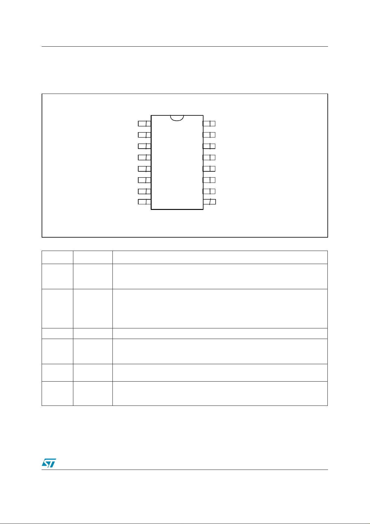
1.1 Functional Description
Figure 1. Block Diagram
OCH
Monitor
Monitor
OCH
OSC
OSC
+
+
0.6V
LDO
LDO
VCCDR
VCCDR
BOOT
BOOT
HGATE
HGATE
PHASE
PHASE
V
OUT
LGATE
LGATE
-
-
PGND
PGND
GND
GND
+
+
+
PWM
PWM
E/A
E/A
EAREF
EAREF
PGOOD
SYNCH
OCL
OCL
Protection and Ref
Protection and Ref
FB
COMP
COMP
5/32
2 Electrical Data L6732C
2 Electrical Data
2.1 Maximum Rating
Tab le 1. Absolute maximum ratings
Symbol Parameter Value Unit
V
VCC to GND and PGND, OCH, PGOOD
CC
V
BOOT - VPHASE
V
HGATE - VPHASE
V
BOOT
V
PHASE
Boot V oltage 0 to 6 V
BOOT -0.3 to 24 V
PHASE -1 to 18
PHASE Sp ike, transient < 50ns (F
= 500KHz)
SW
-0.3 to 18 V
0 to V
BOOT
- V
PHASE
-3
+24
V
V
OCH Pin
SS, FB, EAREF, SYNC, OCL, LGATE, COM P, V
Maximum Withstanding Voltage Range
CCDR
-0.3 to 6 V
±1500
Test Condition: CDF-AEC-Q100- 002 "Human Body Model"
OTHER PINS ±2000
Acceptance Cri teria: "Normal Performance"
2.2 Thermal Data
Table 2. Thermal data
Symbol Description Value Unit
(1)
R
thJA
T
STG
T
J
T
A
1. Package mounted on demoboard.
Max. Thermal Resistance Junction to ambient 50 °C/W
Storage temperature range -40 to 150 °C
Junction operating temperature range -40 to 125 °C
Operative tempera tur e range -25 ~ +125 °C
VPGOOD Pin ±1000
6/32
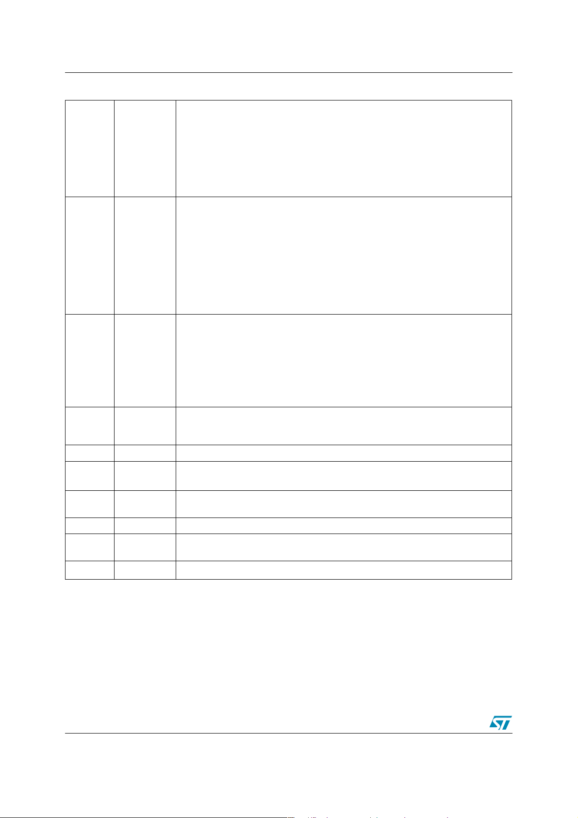
L6732C 3 Pin Connections and Functions
2 3 4
6
12
14 15 16
10
8
OCL
3 Pin Connectio ns and Functions
Figure 2. Pins Connection ( Top view)
PGOOD
SYNCH
1
SGND
FB
COMP
SS/INH
EAREF
Table 3. Pin Functions
Pin n. Name Function
This pin is an open collector output and it is pull ed low if the output voltage is not
1 PGOOD
2 SYNCH
within the specified thresholds (90%-1 10% ). If not used it may be lef t floating. Pull-up
this pin to V
It is a Master-Slave pin. Two or more devices can be synchronized by simply
connecting the SYNCH pins together. The device operating with the highest F
be the Master. The Slave devic es wil l operate with 180° pha se shift from the Master.
The best way to synchronize devic es toget her is to set thei r FSW at the same valu e. If
it is not used the SYNCH pin can be left floati ng.
5
7
HTSSOP16
with a 10K resistor to obtain a logical signal.
CCDR
13
11
9
VCC
VCCDR
LGATE
PGND
BOOT
HGATE
PHASE
OCH
SW
will
3 SGND All the inter nal references are referred to this pin.
This pin is connected to the error amplifier inverting input. Connect it to V
4 FB
5 COMP
6 SS/INH
the compensation net work. This pin is also used to sense the output volt age in order
to manage the over voltage conditions and the PGood signal.
This pin is connected to t he error amplifier output and is used to compensate the
voltage control feedback loop.
The soft-st art time is program m ed connecting an external capacitor fr om this pin and
GND. The internal current generator forces a current of 10 A through t he capacitor.
When the vol tage at this pin is lower than 0.5V the device is disabled.
OUT
through
7/32
3 Pin Connections and Functions L6732C
S
---
---
Table 3. Pin Functions
By setting the voltage at this pin is possible to select the internal /external re ference
and the switching frequency:
7 EAREF
8 OCL
9 OCH
0-80% of V
V
EAREF
V
V
= 80%-95% of V
EAREF
= 95%-100% of V
EAREF
An internal clamp limits the maximum V
analog value presen t at this pin at the start-up when V
A resistor connec ted f rom this pin to ground se ts the valley- current-limit. The valley
current is sensed through the low-side MOSFET(s). The internal current generator
sources a current of 100µA (I
(R
). The over- current threshold i s given by the following equation:
OCL
Connecting a capacitor from this pin to GND helps in reducing the noise injected from
to the device, but can be a low impedanc e path for the high-frequency noise
V
CC
related to the GND. Connect a cap acitor only to a "clean" GND.
A resistor connected from this pin and the high-side MOSFET(s) dr ain sets the peak-
current-limit . The peak current is sensed through the high-si de MOSFET(s). The
internal 100µA current generator (I
external resistor (R
equation:
-> External Reference/FSW=250KHz
CCDR
-> V
CCDR
CCDR -> VREF
OCL
). The over-current threshold i s giv en by the following
OCH
= 0.6V/FSW=500KHz
REF
= 0.6V/FSW=250KHz
at 2.5V (typ.). The devi ce captures the
EAREF
meets the UVLO threshol d.
CC
) from this pin to ground through the external resistor
I
•
I
VALLEY
OCH
I
PEAK
OCLIOCL
=
----------------------------2R
•
DSONL
) sinks a current fro m the drai n through the
I
•
OCHROCH
------------------------------
=
R
DSONHS
This pin is connected to t he source of the high-side MOSFET(s) and provides the
10 PHASE
return path for the high-side dr iver. This pin monitors the drop across both the upper
and lower MOSFET(s) for the current li m it together with OCH and OCL.
1 1 HGATE This pin is connected to the high-side MOSFET(s) gat e.
12 BOOT
13 PGND
Through this pin is supplied the high-side driver. Connect a capacitor from this pin to
the PHASE pin and a diode from V
to this pin (cathode versus BOOT).
CCDR
This pin has to be connected closely to the low-side MOSFET(s) source in order to
reduce the noise injection into the device.
14 LGATE This pin is connected to t he low-side MOSFET(s) gate.
15
16
V
CCDR
V
CC
5V internally regulated voltage. It is used to supply the inter nal drivers. Fil ter it to
ground with at least 1µF ceramic cap.
Supply voltag e pin. The operative supply voltage range is from 4.5V to 14V.
8/32
L6732C 4 Electrical Char acteristics
4 Electrical Characteristics
V
= 12V, TA = 25°C unless otherwise specified.
CC
Table 4. Electrical Characteristics
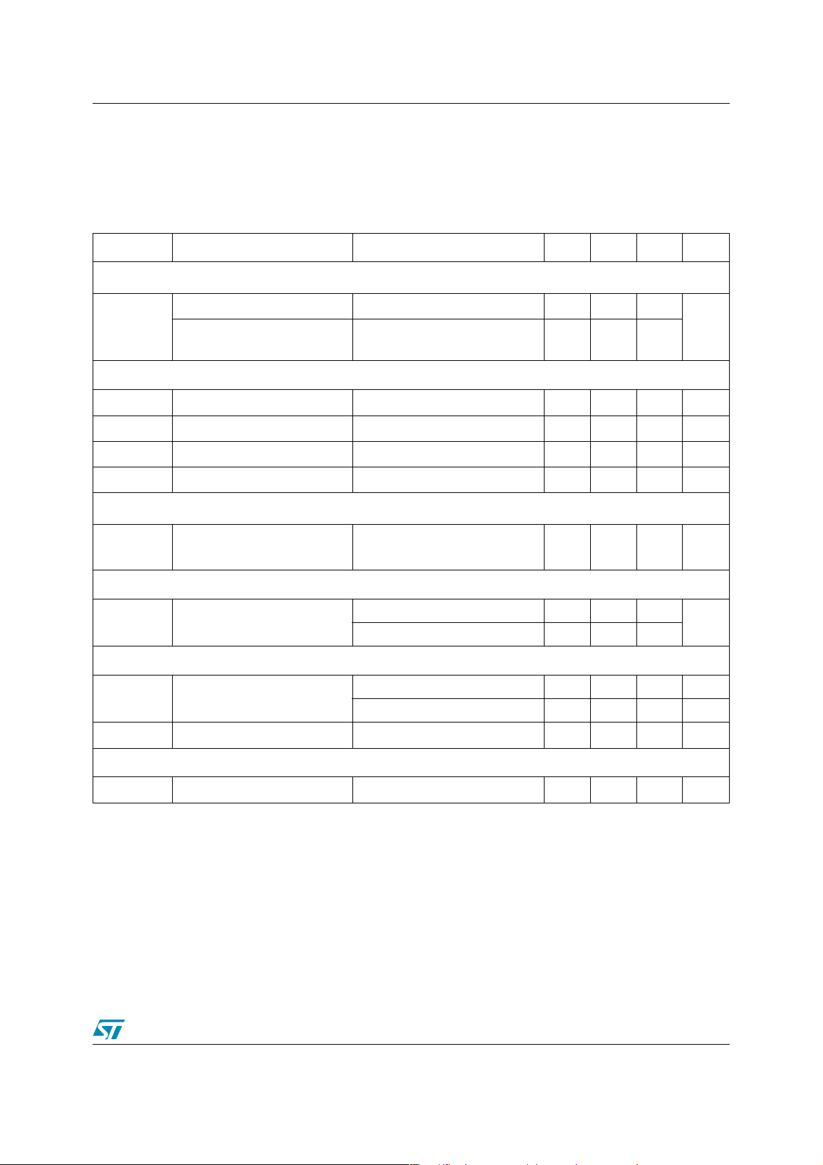
Symbol Parameter Test Condition Min. Typ. Max. Unit
V
Supply Current
CC
VCC Stand By current
I
CC
quiescent current
V
CC
Power-ON
V
CC
Turn-ON VCC thresh o ld V
Turn-OFF V
V
CCDR
V
V
IN OK
IN OK
Regulation
Turn-ON V
Turn-OFF V
V
CCDR
Soft Start and Inhibit
I
SS
Soft Start Current
Oscillator
f
OSC
Accuracy
CC
OCH
OCH
voltage
threshold V
thresh ol d
threshold
OSC = open; SS to GND 4.5 6.5
OSC= open;
HG = open, LG = open, PH=open
= 1.7V
OCH
= 1.7V
OCH
4.0 4.2 4.4 V
3.6 3.8 4.0 V
8.5 10
1.1 1.25 1.47 V
0.9 1.05 1.27 V
=5.5V to 14V
V
CC
= 1mA to 100mA
I
DR
4.5 5 5.5 V
SS = 2V 7 10 13
SS = 0 to 0.5V 20 30 45
237 250 263 KHz
450 500 550 KHz
mA
µA
∆V
OSC
Output Voltage
V
FB
Ramp Amplitude 2.1 V
= 0 to Vth
Output Voltage
V
DIS
0.597 0.6 0.603 V
9/32

L6732C
Table 4. Electri cal C harac teris tics
Symbol Parameter Test Condition Min. Typ. Max. Unit
Error Amplifier
R
EAREF
I
FB
Ext Ref
Clamp
V
OFFSET
G
V
EAREF Input Resistance Vs. GND 70 100 150 kΩ
I.I. bias current
V
FΒ
0.290 0.5 µA
= 0V
2.3 V
Error amplifier offset Vref = 0.6V -5 +5 mV
Open Loop Voltage Gain Guaranteed by design 100 dB
GBWP Gain-Bandwidth Product Guaranteed by design 10 MHz
SR Slew-Rate
COMP = 10pF
Gua r anteed by desig n
5V/µs
Gate Drivers
R
HGATE_ON
R
HGATE_OFF
R
LGATE_ON
R
LGATE_OFF
High Side Sour ce Resistance
High Side Sink Resistance
Low Side Source Resistance
Low Side Sink Resistance
BOOT
V
BOOT
V
CCDR
V
CCDR
- V
- V
= 5V
= 5V
PHASE
PHASE
= 5V
= 5V
1.7 Ω
1.12 Ω
1.15 Ω
0.6 Ω
V
Protections
I
OCH
I
OCL
OVP
OCH Current Source
OCL Current Source 90 100 110 µΑ
Over Voltage Trip
(VFB / VEAREF)
V
OCH
V
FB
V
EAREF
V
FB
V
EAREF
= 1.7V
Rising
= 0.6V
Falling
= 0.6V
90 100 110 µΑ
120 %
117 %
Power Good
V
PGOOD
Upper Threshold
(V
FB
/ V
EAREF
)
Lower Threshold
(V
FB
/ V
EAREF
)
PGOOD Voltage Low IPGOOD = -5mA 0.5 V
V
FB
V
FB
Rising
Falling
108 110 112 %
88 90 92 %
Table 5. Therm al Character istics (VCC = 12V)
Symbol Parameter Test Condition Min. Typ. Max. Unit
Output Voltage
= 0°C~ 125°C
T
V
FB
Output Voltage
J
T
= -40°C~ 125°C
J
0.596 0.6 0.605
V
0.593 0.6 0.605
10/32
 Loading...