

Digitally controlled dual PWM with embedded drivers for VR12
VFQFPN56 - 7x7mm
Features
■ VR12 compliant with 25 MHz SVID bus rev. 1.5
■ Second generation LTB Technology
Very compact dual controller:
■
– Up to 4 phases for core section with 2
internal drivers
– 1 phase for GFX section with internal driver
■ Input voltage up to 12 V
■ SMBus interface for power management
■ SWAP, Jmode, multi-rail only support
■ Programmable offset voltage
■ Single NTC design for TM, LL and IMON
thermal compensation (for each section)
■ VFDE for efficiency optimization
■ DPM - dynamic phase management
■ Dual differential remote sense
■ 0.5% output voltage accuracy
■ Full-differential current sense across DCR
■ AVP - adaptive voltage positioning
■ Programmable switching frequency
■ Dual current monitor
■ Pre-biased output management
■ High-current embedded drivers optimized for
7 V operation
■ OC, OV, UV and FB disconnection protection
■ Dual VR_READY
■ VFQFPN56 7x7 mm package with exposed
pad
Applications
■ High-current VRM / VRD for desktop / server /
new generation workstation CPUs
■ DDR3 DDR4 memory supply for VR12
™
L6718
processors
Datasheet − preliminary data
Description
The L6718 is a very compact, digitally controlled
and cost effective dual controller designed to
power Intel
pinstrapping is used to program the main
parameters.
The device features from 2 to 4-phase
programmable operation for the core section
providing 2 embedded drivers. A single-phase
with embedded driver and with independent
control loop is used for GFX.
The L6718 supports power state transitions
featuring VFDE and a programmable DPM,
maintaining the best efficiency over all loading
conditions without compromising transient
response.
Second generation LTB Technology
minimal cost output filter providing fast load
transient response. The controller assures fast
and independent protection against load
overcurrent, under/overvoltage and feedback
disconnections.
The device is available in VFQFPN56, 7x7 mm
compact package with exposed pad.
Table 1. Device summary
Order code Package Packaging
L6718
L6718TR
®
VR12 processors. Dedicated
™
allows a
VFQFPN56 7x7mm Tray
VFQFPN56 7x7mm
Tape and
reel
July 2012 Doc ID 023399 Rev 1 1/71
This is preliminar y information on a new product now in development or undergoing evaluation. Details are subject to
change without notice.
www.st.com
71

Contents L6718
Contents
1 Typical application circuit and block diagram . . . . . . . . . . . . . . . . . . . . 7
1.1 Application circuit . . . . . . . . . . . . . . . . . . . . . . . . . . . . . . . . . . . . . . . . . . . . 7
1.2 Block diagram . . . . . . . . . . . . . . . . . . . . . . . . . . . . . . . . . . . . . . . . . . . . . . 10
2 Pin description and connection diagrams . . . . . . . . . . . . . . . . . . . . . . 11
2.1 Pin description . . . . . . . . . . . . . . . . . . . . . . . . . . . . . . . . . . . . . . . . . . . . . 12
2.2 Thermal data . . . . . . . . . . . . . . . . . . . . . . . . . . . . . . . . . . . . . . . . . . . . . . 19
3 Electrical specifications . . . . . . . . . . . . . . . . . . . . . . . . . . . . . . . . . . . . . 20
3.1 Absolute maximum ratings . . . . . . . . . . . . . . . . . . . . . . . . . . . . . . . . . . . . 20
3.2 Electrical characteristics . . . . . . . . . . . . . . . . . . . . . . . . . . . . . . . . . . . . . . 20
4 VID tables . . . . . . . . . . . . . . . . . . . . . . . . . . . . . . . . . . . . . . . . . . . . . . . . . 24
5 Device description and operation . . . . . . . . . . . . . . . . . . . . . . . . . . . . . 26
6 Device configuration . . . . . . . . . . . . . . . . . . . . . . . . . . . . . . . . . . . . . . . . 28
6.1 CPU mode . . . . . . . . . . . . . . . . . . . . . . . . . . . . . . . . . . . . . . . . . . . . . . . . 28
6.2 DDR mode . . . . . . . . . . . . . . . . . . . . . . . . . . . . . . . . . . . . . . . . . . . . . . . . 28
6.3 SWAP mode . . . . . . . . . . . . . . . . . . . . . . . . . . . . . . . . . . . . . . . . . . . . . . . 29
6.3.1 MRO - multi-phase rail only . . . . . . . . . . . . . . . . . . . . . . . . . . . . . . . . . . 29
6.4 Jmode . . . . . . . . . . . . . . . . . . . . . . . . . . . . . . . . . . . . . . . . . . . . . . . . . . . 30
6.5 Phase number configuration . . . . . . . . . . . . . . . . . . . . . . . . . . . . . . . . . . 30
6.6 Pinstrapping configuration . . . . . . . . . . . . . . . . . . . . . . . . . . . . . . . . . . . . 31
6.6.1 CONFIG0 in CPU mode . . . . . . . . . . . . . . . . . . . . . . . . . . . . . . . . . . . . 32
6.6.2 CONFIG0 in DDR mode (STCOMP=GND) . . . . . . . . . . . . . . . . . . . . . . 34
6.6.3 CONFIG1 in CPU mode . . . . . . . . . . . . . . . . . . . . . . . . . . . . . . . . . . . . 36
6.6.4 CONFIG1 in DDR mode (STCOMP=GND) . . . . . . . . . . . . . . . . . . . . . . 37
6.6.5 CONFIG2 . . . . . . . . . . . . . . . . . . . . . . . . . . . . . . . . . . . . . . . . . . . . . . . . 39
6.6.6 CONFIG3 . . . . . . . . . . . . . . . . . . . . . . . . . . . . . . . . . . . . . . . . . . . . . . . . 40
7 L6718 power manager . . . . . . . . . . . . . . . . . . . . . . . . . . . . . . . . . . . . . . . 42
7.1 SMBus power manager . . . . . . . . . . . . . . . . . . . . . . . . . . . . . . . . . . . . . . 42
2/71 Doc ID 023399 Rev 1

L6718 Contents
7.1.1 SMBus sequence . . . . . . . . . . . . . . . . . . . . . . . . . . . . . . . . . . . . . . . . . . 43
7.2 SMBus tables . . . . . . . . . . . . . . . . . . . . . . . . . . . . . . . . . . . . . . . . . . . . . . 43
7.3 DPM . . . . . . . . . . . . . . . . . . . . . . . . . . . . . . . . . . . . . . . . . . . . . . . . . . . . . 47
7.4 VFDE . . . . . . . . . . . . . . . . . . . . . . . . . . . . . . . . . . . . . . . . . . . . . . . . . . . . 48
7.5 Power state indicator (PSI) . . . . . . . . . . . . . . . . . . . . . . . . . . . . . . . . . . . . 49
8 Output voltage positioning . . . . . . . . . . . . . . . . . . . . . . . . . . . . . . . . . . . 50
8.1 Multi-phase section - current reading and current sharing loop . . . . . . . . 50
8.2 Multi-phase section - defining load-line . . . . . . . . . . . . . . . . . . . . . . . . . . 51
8.3 Single-phase section - current reading . . . . . . . . . . . . . . . . . . . . . . . . . . . 52
8.4 Single-phase section - defining load-line . . . . . . . . . . . . . . . . . . . . . . . . . 52
8.5 Dynamic VID transition support . . . . . . . . . . . . . . . . . . . . . . . . . . . . . . . . 53
8.6 DVID optimization: REF/SREF . . . . . . . . . . . . . . . . . . . . . . . . . . . . . . . . . 53
9 Output voltage monitoring and protection . . . . . . . . . . . . . . . . . . . . . . 55
9.1 Overvoltage . . . . . . . . . . . . . . . . . . . . . . . . . . . . . . . . . . . . . . . . . . . . . . . 55
9.2 Overcurrent . . . . . . . . . . . . . . . . . . . . . . . . . . . . . . . . . . . . . . . . . . . . . . . 56
9.2.1 Multi-phase section . . . . . . . . . . . . . . . . . . . . . . . . . . . . . . . . . . . . . . . . 56
9.2.2 Overcurrent and power states . . . . . . . . . . . . . . . . . . . . . . . . . . . . . . . . 57
9.2.3 Single-phase section . . . . . . . . . . . . . . . . . . . . . . . . . . . . . . . . . . . . . . . 58
10 Single NTC thermal monitor and compensation . . . . . . . . . . . . . . . . . 59
10.1 Thermal monitor and VR_HOT . . . . . . . . . . . . . . . . . . . . . . . . . . . . . . . . . 59
10.2 Thermal compensation . . . . . . . . . . . . . . . . . . . . . . . . . . . . . . . . . . . . . . . 60
10.3 TM and TCOMP design . . . . . . . . . . . . . . . . . . . . . . . . . . . . . . . . . . . . . . 60
11 Main oscillator . . . . . . . . . . . . . . . . . . . . . . . . . . . . . . . . . . . . . . . . . . . . . 61
12 System control loop compensation . . . . . . . . . . . . . . . . . . . . . . . . . . . 62
12.1 Compensation network guidelines . . . . . . . . . . . . . . . . . . . . . . . . . . . . . . 63
12.2 LTB technology . . . . . . . . . . . . . . . . . . . . . . . . . . . . . . . . . . . . . . . . . . . . . 64
13 Power dissipation and application details . . . . . . . . . . . . . . . . . . . . . . 65
13.1 High-current embedded drivers . . . . . . . . . . . . . . . . . . . . . . . . . . . . . . . . 65
13.2 Boot diode and capacitor design . . . . . . . . . . . . . . . . . . . . . . . . . . . . . . . 65
Doc ID 023399 Rev 1 3/71

Contents L6718
13.3 Device power dissipation . . . . . . . . . . . . . . . . . . . . . . . . . . . . . . . . . . . . . 65
14 Layout guidelines . . . . . . . . . . . . . . . . . . . . . . . . . . . . . . . . . . . . . . . . . . 67
14.1 Power components and connections . . . . . . . . . . . . . . . . . . . . . . . . . . . . 67
14.2 Small signal components and connections . . . . . . . . . . . . . . . . . . . . . . . 67
15 Package mechanical data . . . . . . . . . . . . . . . . . . . . . . . . . . . . . . . . . . . . 68
16 Revision history . . . . . . . . . . . . . . . . . . . . . . . . . . . . . . . . . . . . . . . . . . . 70
4/71 Doc ID 023399 Rev 1

L6718 List of tables
List of tables
Table 1. Device summary . . . . . . . . . . . . . . . . . . . . . . . . . . . . . . . . . . . . . . . . . . . . . . . . . . . . . . . . . . 1
Table 2. Pin description . . . . . . . . . . . . . . . . . . . . . . . . . . . . . . . . . . . . . . . . . . . . . . . . . . . . . . . . . . 12
Table 3. Thermal data. . . . . . . . . . . . . . . . . . . . . . . . . . . . . . . . . . . . . . . . . . . . . . . . . . . . . . . . . . . . 19
Table 4. Absolute maximum ratings . . . . . . . . . . . . . . . . . . . . . . . . . . . . . . . . . . . . . . . . . . . . . . . . . 20
Table 5. Electrical characteristics . . . . . . . . . . . . . . . . . . . . . . . . . . . . . . . . . . . . . . . . . . . . . . . . . . . 20
Table 6. VID table, both sections, commanded through serial bus . . . . . . . . . . . . . . . . . . . . . . . . . 24
Table 7. Phase number programming . . . . . . . . . . . . . . . . . . . . . . . . . . . . . . . . . . . . . . . . . . . . . . . 31
Table 8. CONFIG0/PSI0 pinstrapping in CPU MODE . . . . . . . . . . . . . . . . . . . . . . . . . . . . . . . . . . . 33
Table 9. CONFIG0/PSI0 pinstrapping in DDR MODE . . . . . . . . . . . . . . . . . . . . . . . . . . . . . . . . . . . 34
Table 10. CONFIG1/PSI1 pinstrapping in CPU MODE . . . . . . . . . . . . . . . . . . . . . . . . . . . . . . . . . . . 36
Table 11. CONFIG1/PSI1 pinstrapping in DDR MODE . . . . . . . . . . . . . . . . . . . . . . . . . . . . . . . . . . . 37
Table 12. CONFIG2/SDA pinstrapping . . . . . . . . . . . . . . . . . . . . . . . . . . . . . . . . . . . . . . . . . . . . . . . . 39
Table 13. CONFIG3/SCL pinstrapping . . . . . . . . . . . . . . . . . . . . . . . . . . . . . . . . . . . . . . . . . . . . . . . . 40
Table 14. SMBus addressing . . . . . . . . . . . . . . . . . . . . . . . . . . . . . . . . . . . . . . . . . . . . . . . . . . . . . . . 43
Table 15. SMBus interface commands. . . . . . . . . . . . . . . . . . . . . . . . . . . . . . . . . . . . . . . . . . . . . . . . 44
Table 16. SMBus VID . . . . . . . . . . . . . . . . . . . . . . . . . . . . . . . . . . . . . . . . . . . . . . . . . . . . . . . . . . . . . 45
Table 17. Power status . . . . . . . . . . . . . . . . . . . . . . . . . . . . . . . . . . . . . . . . . . . . . . . . . . . . . . . . . . . . 49
Table 18. L6718 protection at a glance . . . . . . . . . . . . . . . . . . . . . . . . . . . . . . . . . . . . . . . . . . . . . . . 55
Table 19. Multi-phase section OC scaling and power states . . . . . . . . . . . . . . . . . . . . . . . . . . . . . . . 58
Table 20. VFQFPN56 7x7 mechanical data . . . . . . . . . . . . . . . . . . . . . . . . . . . . . . . . . . . . . . . . . . . . 68
Table 21. Document revision history . . . . . . . . . . . . . . . . . . . . . . . . . . . . . . . . . . . . . . . . . . . . . . . . . 70
Doc ID 023399 Rev 1 5/71

List of figures L6718
List of figures
Figure 1. Typical 4-phase application circuit . . . . . . . . . . . . . . . . . . . . . . . . . . . . . . . . . . . . . . . . . . . . 7
Figure 2. Typical 3-phase application circuit . . . . . . . . . . . . . . . . . . . . . . . . . . . . . . . . . . . . . . . . . . . . 8
Figure 3. Typical 2-phase application circuit . . . . . . . . . . . . . . . . . . . . . . . . . . . . . . . . . . . . . . . . . . . . 9
Figure 4. Block diagram . . . . . . . . . . . . . . . . . . . . . . . . . . . . . . . . . . . . . . . . . . . . . . . . . . . . . . . . . . . 10
Figure 5. Pin connection (top view) . . . . . . . . . . . . . . . . . . . . . . . . . . . . . . . . . . . . . . . . . . . . . . . . . . 11
Figure 6. Device initialization . . . . . . . . . . . . . . . . . . . . . . . . . . . . . . . . . . . . . . . . . . . . . . . . . . . . . . . 27
Figure 7. SWAP mode . . . . . . . . . . . . . . . . . . . . . . . . . . . . . . . . . . . . . . . . . . . . . . . . . . . . . . . . . . . . 29
Figure 8. SMBus communication format . . . . . . . . . . . . . . . . . . . . . . . . . . . . . . . . . . . . . . . . . . . . . . 43
Figure 9. Output current vs. switching frequency in PSK mode. . . . . . . . . . . . . . . . . . . . . . . . . . . . . 48
Figure 10. Voltage positioning . . . . . . . . . . . . . . . . . . . . . . . . . . . . . . . . . . . . . . . . . . . . . . . . . . . . . . . 50
Figure 11. Current reading . . . . . . . . . . . . . . . . . . . . . . . . . . . . . . . . . . . . . . . . . . . . . . . . . . . . . . . . . . 51
Figure 12. DVID optimization circuit. . . . . . . . . . . . . . . . . . . . . . . . . . . . . . . . . . . . . . . . . . . . . . . . . . . 54
Figure 13. Thermal monitor connections . . . . . . . . . . . . . . . . . . . . . . . . . . . . . . . . . . . . . . . . . . . . . . . 59
Figure 14. ROSC [KOhm] vs. switching frequency [kHz] per phase. . . . . . . . . . . . . . . . . . . . . . . . . . . 61
Figure 15. Equivalent control loop. . . . . . . . . . . . . . . . . . . . . . . . . . . . . . . . . . . . . . . . . . . . . . . . . . . . 62
Figure 16. Control loop Bode diagram and fine tuning. . . . . . . . . . . . . . . . . . . . . . . . . . . . . . . . . . . . . 63
Figure 17. VFQFPN56 7x7 package dimensions. . . . . . . . . . . . . . . . . . . . . . . . . . . . . . . . . . . . . . . . . 69
6/71 Doc ID 023399 Rev 1
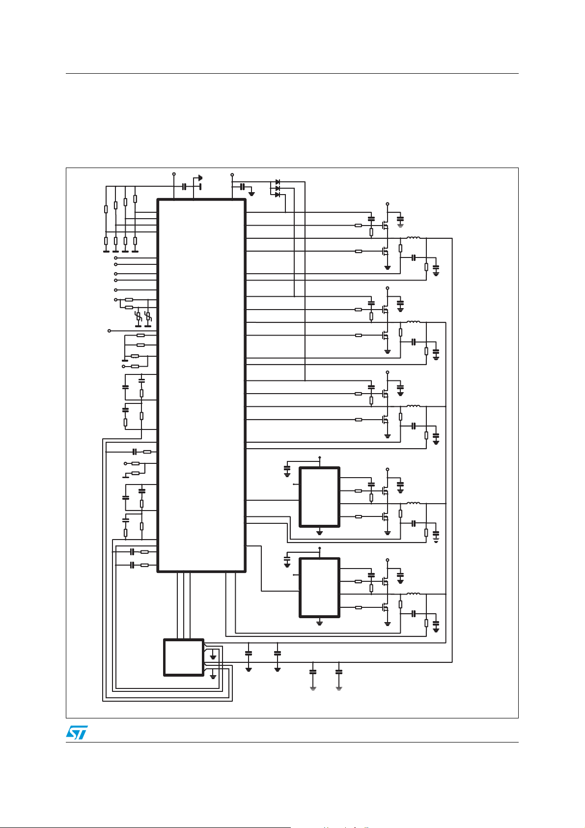
L6718 Typical application circuit and block diagram
LS1
L1
CHF
Rtcm
Ctcm
+12V
Rg
BOOT
UGATE
PHASE
LGATE
VCC
L6743
EN
PWM4
CS3P
SC3N
SCSP
SCSN
SBOOT
VR12 μP LOAD
CORE
VR12 SVID
C
SOUTCSMLCC
PWM
GND
CDEC
SVCLK
ALERT#
SVDATA
CF
RF
CI
RI
RFB
CP
RGND
VSEN
FB
COMP
IMON
CSF
RSF
CSI
RSI
RSFB
CSP
SRGND
SVSEN
SFB
SCOMP
SIMON
CLTB RLTB
LTB
SPHASE
+7V
VCC5
+5V
GND
(PAD)
VR_HOT
EN
REF
SREF/JEN
+5V
ST L6718
ST L6718 (4+1) Reference Schematic
C
OUT
C
MLCC
HS1
LSs
Ls
CHF
Rtcm_s
Ctcm_s
+12V
Rg_s
HSs
LS2
L2
CHF
Rtcm
Ctcm
+12V
Rg
HS2
LS3
L3
CHF
Rtcm
Ctcm
+12V
Rg
HS3
LS4
L4
CHF
Rtcm
Ctcm
+12V
RG
HS4
+12V
BOOT
UGATE
PHASE
LGATE
VCC
L6743
EN
PWM
GND
CDEC
+12V
PWM3
SLGATE
SHGATE
CS1P
CS1N
BOOT1
PHASE1
LGATE1
HGATE1
CS2P
CS2N
BOOT2
PHASE2
LGATE2
HGATE2
CS4P
CS4N
OSC/FLT
SOSC/SFLT
ENABLE
SVREADY
VREADY
VRHOT
TM
CONF1/PSI1
TCOMP
STCOMP/DDR
CONF0/PSI0
SCL/CONFIG3
SDA/CONFIG2
VCC12
GPU
RSIMON
+5V
CSREF RSREF
CREF
RREF
RIMON
STM
RGate
RGate
RGate
RGate
RGate
RGate
RGate
RGate
RGate
RGate
Rboot
Rboot
Rboot
Rboot
Rboot
Cboot
Cboot
Cboot
Cboot
Cboot
AM12875v1
1 Typical application circuit and block diagram
1.1 Application circuit
Figure 1. Typical 4-phase application circuit
Doc ID 023399 Rev 1 7/71
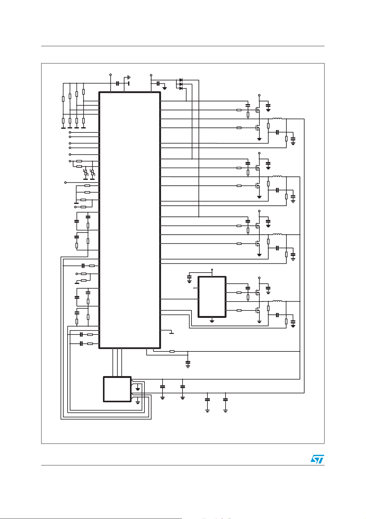
Typical application circuit and block diagram L6718
LS1
L1
CHF
Rtcm
Ctcm
+12V
Rg
BOOT
UGATE
PHASE
LGATE
VCC
L6743B
EN
PWM4
CS3P
SC3N
SCSP
SCSN
SBOOT
VR12 μP LOAD
CORE
VR12 SVID
C
SOUTCSMLCC
PWM
GND
CDEC
SVCLK
ALERT#
SVDATA
CF
RF
CI
RI
RFB
CP
RGND
VSEN
FB
COMP
IMON
CSF
RSF
CSI
RSI
RSFB
CSP
SRGND
SVSEN
SFB
SCOMP
SIMON
CLTB RLTB
LTB
SPHASE
+7V
VCC5
+5V
GND
(PAD)
EN
REF
SREF/JEN
+5V
ST L6718
ST L6718 (3+1) Reference Schematic
C
OUT
C
MLCC
HS1
LSs
Ls
CHF
+12V
Rg_s
HSs
LS2
L2
CHF
+12V
HS2
LS2
L3
CHF
+12V
HS3
+12V
PWM3
SLGATE
SHGATE
CS1P
CS1N
BOOT1
PHASE1
LGATE1
HGATE1
CS2P
CS2N
BOOT2
PHASE2
LGATE2
HGATE2
CS4N
CS4P
OSC/OVP
SOSC/SOVP
ENABLE
SVREADY
VREADY
VRHOT
TM
CONF1/PSI1
TCOMP
STCOMP/DDR
CONF0/PSI0
SCL/CONFIG3
SDA/CONFIG2
VCC12
GPU
RSIMON
+5V
CSREF RSREF
CREF RREF
RIMON
STM
Rtcm_s
Ctcm_s
RGate
RGate
Rboot
Cboot
RGate
RGate
Rboot
Cboot
RGate
RGate
Rboot
Cboot
RGate
RGate
Rboot
Cboot
Rtcm
Ctcm
Rg
Rtcm
Ctcm
Rg
AM12876v1
Figure 2. Typical 3-phase application circuit
8/71 Doc ID 023399 Rev 1
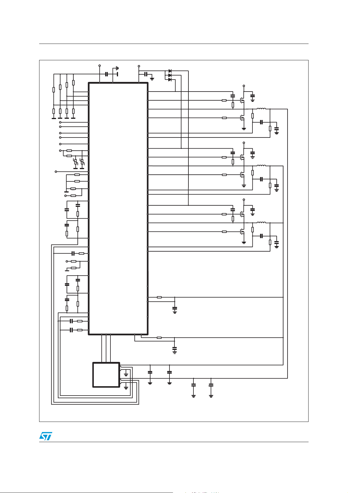
L6718 Typical application circuit and block diagram
LS2
L1
CHF
+12V
PWM4
CS3N
SC3P
SCSP
SCSN
SBOOT
VR12 μP LOAD
CORE
VR12 SVID
C
SOUTCSMLCC
SVCLK
ALERT#
SVDATA
CF
RF
CI
RI
RFB
CP
RGND
VSEN
FB
COMP
IMON
CSF
RSF
CSI
RSI
RSFB
CSP
SRGND
SVSEN
SFB
SCOMP
SIMON
CLTB RLTB
LTB
SPHASE
+7V
VCC5
+5V
GND
(PAD)
EN
REF
SREF/JEN
+5V
ST L6718
ST L6718 (2+1) Reference Schematic
C
OUT
C
MLCC
HS1
LSs
Ls
CHF
+12V
HSs
LS2
L2
CHF
+12V
HS2
PWM3
SLGATE
SHGATE
CS1P
CS1N
BOOT1
PHASE1
LGATE1
HGATE1
CS2P
CS2N
BOOT2
PHASE2
LGATE2
HGATE2
CS4N
CS4P
OSC/FLT
SOSC/SFLT
ENABLE
SVREADY
VREADY
VRHOT
TM
CONF1/PSI1
TCOMP
STCOMP/DDR
CONF0/PSI0
SCL/CONFIG3
SDA/CONFIG2
VCC12
GPU
RSIMON
+5V
CSREF RSREF
CREF RREF
RIMON
STM
Rtcm_s
Ctcm_s
Rg_s
Rtcm
Ctcm
Rg
Rtcm
Ctcm
Rg
RGate
RGate
Rboot
Cboot
RGate
RGate
Rboot
Cboot
RGate
RGate
Rboot
Cboot
Rg
Rg
AM12877v1
Figure 3. Typical 2-phase application circuit
Doc ID 023399 Rev 1 9/71
Typical application circuit and block diagram L6718
PWM4
PWM3
PWM2
PWM1
LTB Technology
Modulator
& Frequency Limiter
Ramp & Clock
Generator
with VFDE
S
S
S
S
Differential Current Sense
Current Balance
& Peak Curr Limit
Thermal
Compensation
and Gain adjust
CS1P
CS1N
CS2P
CS2N
CS3P
CS3N
CS4P
CS4N
LTB
ERROR
AMPLIFIER
TM
TCOMP
VRHOT
I
MON
I
DROOP
OCP
VR12 Bus Manager
FB
REF
COMP
SVD ATA
ALERT#
SVCLK
IMON
Dual DAC & Ref
Generator
VR12 Registers
CONFIG1/PSI1
CONFIG0/PSI0
RGND
VSEN
OV
+OVP_Trk
MultiPhase
Fault Manager
OC
SREF
Thermal
Sensing
and Monitor
TempZone
TempZone
Imon
SImon
Chan #
LTB Technology
Modulator
& Frequency Limiter
Ramp & Clock
Generator
withVFDE
SOSC/SFLT
SHGATE
SPWM
ERROR
AMPLIFIER
I
SMON
I
SDROOP
OCP
SFB
SREF/JEN
SCOMP
SIMON
SRGND
SVSEN SOV
+OVP_Trk
SOC
SREF
SinglePhase
Fault Manager
VREADY
FLT
FLT
To SinglePhase
FLT Manager
To M ultiPhase FLT Manage
SVREADY
SFLT
SFLT
DDR
Differential
Current Sense
SCSP
SCSN
Start-up Logic
VCC12
VCC5
ENABLE
S_EN
EN
S_EN
GND (PAD)
OSC /FLT
VSEN
I
REF
I
REF
I
SREF
I
SREF
STM
Thermal
Compensation
and Gain adjust
STCOMP/DDR
VCC12
SBOOT
SPHASE
SLGATE
SWAP
Anti Cross
Conduction
Anti Cross
Conduction
Anti Cross
Conduction
SDA/CONF2
SCL/CONF3
SMBus
Manager
SWAP
DDRTh
PWM4/PH#N
PMW3/SPWM
LGATE2
PHASE2
HGATE2
BOOT2
LGATE1
PHASE1
HGATE1
BOOT1
PH#N
L6718
JEN
AM12878v1
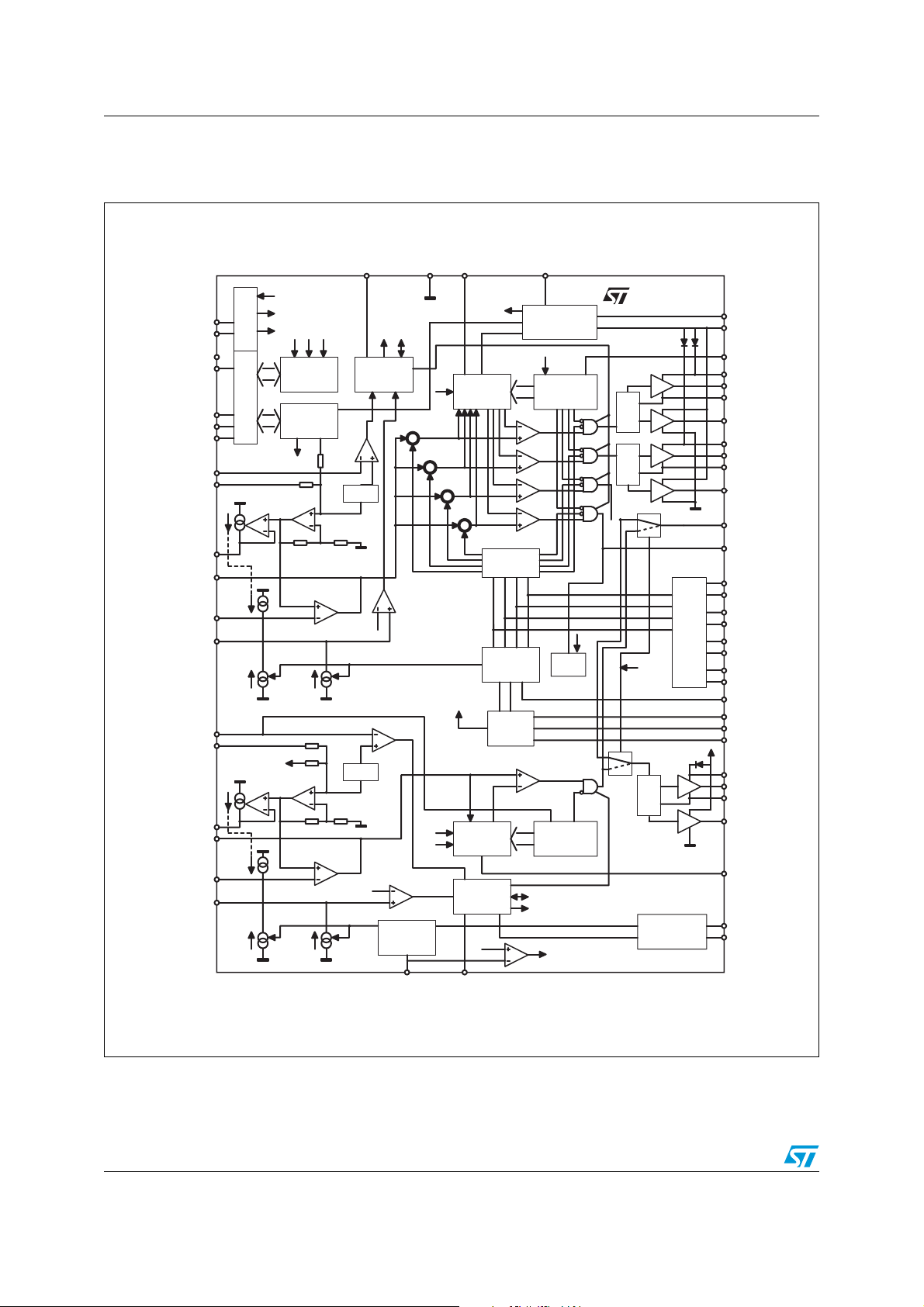
1.2 Block diagram
Figure 4. Block diagram
10/71 Doc ID 023399 Rev 1
L6718 Pin description and connection diagrams
12
11
10
9
8
7
6
5
4
3
2
1
31
32
33
34
35
36
37
38
39
40
41
42
56 55 54 53 52 51 50 49 48 47 46 45
15 16 17 18 19 20 21 22 23 24 25 26
SOSC/SFLT
SCSP
SCSN
STM
CONF0/PSI0
SHGATE
SPHASE
SLGATE
PWM4/PH#
PMW3//SPWM
PHASE1
SBOOT
LT B
VSEN
RGND
ALERT#
SV DATA
SVCLK
VRHOT
TM
CS3N
CS3P
CS1P
CS1N
CS2N
CS2P
CS4P
CS4N
VREADY
SVREADY
LGATE1
LGAE2
PHASE2
HGATE2
BOOT2
VCC12
IMON
REF
SRGND
SVSEN
SFB
SCOMP
SIMON
SREF
ENABLE
STCOMP/DDR
TCOMP
CONF1/PSI1
L6718
27 28
29
30
44 43
14
13
COMP
FB
CONF2/SDA
CONF3/SCL
VCC5
OSC/FLT
BOOT1
HGATE1
AM12879v1
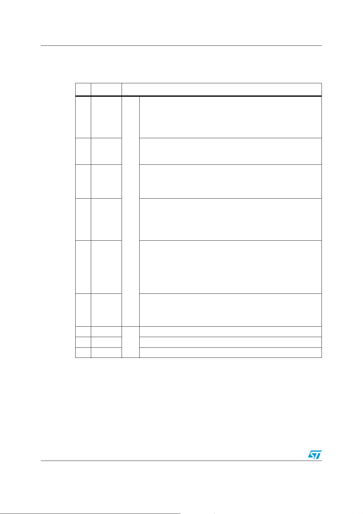
2 Pin description and connection diagrams
Figure 5. Pin connection (top view)
Doc ID 023399 Rev 1 11/71
Pin description and connection diagrams L6718
2.1 Pin description
Table 2. Pin description
Pin# Name Function
Channel 1 current sense negative input.
Connect through an RG resistor to the output-side of channel 1 inductor.
1CS1N
2CS1P
3CS3P
4CS3N
5TM
Filter the output-side of R
with 100 nF (typ.) to GND.
G
This pin is compared with VSEN for the feedback disconnection.
See Section 14 for proper layout of this connection.
Channel 1 current sense positive input.
Connect through an R-C filter to the phase-side of channel 1 inductor.
See Section 14 for proper layout of this connection.
Channel 3 current sense positive input.
Connect through an R-C filter to the phase-side of channel 3 inductor.
Short to V
when not using channel 3.
OUT
See Section 14 for proper layout of this connection.
Channel 3 current sense negative input.
Connect through an R
Filter the output-side of R
Connect to V
See Section 14 for proper layout of this connection.
MULTI-RAIL SECTION
OUT
resistor to the output-side of channel 3 inductor.
G
with 100 nF (typ.) to GND.
G
through an RG resistor when not using channel 3.
Thermal monitor sensor.
Connect with proper network embedding NTC to the multi-phase rail
power section. The IC senses the power section temperature and uses the
information to define the VRHOT signal and temperature zone register.
By programming proper TCOMP gain, the IC also implements load-line
thermal compensation for the multi-phase rail section. See Section 10 for
details.
Voltage regulator HOT.
6 VRHOT
Open drain output, set free by controller when the temperature sensed
through the TM pin exceeds TMAX (active low).
See Section 10.1 for details.
7 SVCLK
Serial clock
8 SVDATA Serial data
9ALERT# Alert
SVID BUS
12/71 Doc ID 023399 Rev 1

L6718 Pin description and connection diagrams
Table 2. Pin description (continued)
Pin# Name Function
Remote ground sense pin.
10 RGND
11 VSEN
12 LTB
13 FB
14 COMP
Connect to the negative side of the load to perform remote sense.
See Section 14 for proper layout of this connection.
Output voltage monitor pin.
Manages OVP/UVP protection and feedback disconnection. Connect to
the positive side of the load to perform remote sense. A fixed 50 uA
current is sourced from this pin.
See Section 14 for proper layout of this connection.
Load transient boost technology input pin.
Internally fixed at 1.67 V, connecting R
LT B
- C
LT B
vs. V
allows the load
OUT
transient boost technology to be enabled, as soon as the device detects a
transient load it turns on all the PHASEs at the same time. Short to SGND
to disable the function.
See Section 12.2 for details.
Error amplifier inverting input.
Connect with an R
to VSEN and (RF - CF)// CP to COMP.
FB
A current proportional to the load current is sourced from this pin in order
to implement the droop effect. See Section 8.2 for details.
MULTI-RAIL SECTION
Error amplifier output.
Connect with (RF - CF)// CP to FB.
The device cannot be disabled by pulling down this pin.
15 IMON
16 REF
Current monitor output.
A current proportional to the multi-phase rail output current is sourced
from this pin. Connect through a resistor R
to GND to show a voltage
IMON
proportional to the current load. Based on pin voltage level, DPM and
overcurrent protection can be triggered. Filtering through C
allows control of the delay. See Section 9.2 for R
IMON
definition.
IMON
to GND
The reference used for the regulation of the multi-phase rail section is
available on this pin with -100 mV + offset. Connect through an R
to RGND to optimize DVID transitions. See Section 8.6 for details.
C
REF
REF
-
Doc ID 023399 Rev 1 13/71

Pin description and connection diagrams L6718
Table 2. Pin description (continued)
Pin# Name Function
Single-phase rail remote ground sense.
17 SRGND
18 SVSEN
19 SFB
20 SCOMP
21 SIMON
22 SREF/JEN
Connect to the negative side of the single-phase rail load to perform
remote sense.
See Section 14 for proper layout of this connection.
Single-rail output voltage monitor.
Manages OVP/UVP protection and feedback disconnection. Connect to
the positive side of the load to perform remote sense. It is also the sense
for the single-phase rail LTB.
Connect to the positive side of the single-phase rail load to perform
remote sense.
See Section 14 for proper layout of this connection.
Error amplifier inverting input.
Connect with a resistor R
to SVSEN and with (RSF - CSF)// CSP to
SFB
SCOMP. A current proportional to the load current is supplied from this pin
in order to implement the droop effect. See Section 8.4 for details.
Error amplifier output.
Connect with an (R
- CSF)// CSP to SFB. The device cannot be disabled
SF
by pulling this pin low.
SINGLE-RAIL SECTION
Current monitor output.
A current proportional to the output current is sourced from this pin.
Connect through a resistor R
overcurrent protection can be triggered. Filtering through C
to local GND. Based on pin voltage,
SIMON
SIMON
allows control of the delay for OC intervention. See Section 9.2 for R
definition.
The reference used for the regulation of the single-rail section is available
on this pin with -100 mV + offset. Connect through an R
SREF-CSREF
SRGND to optimize DVID transitions. See Section 8.6 for details.
If Jmode is selected by Config1 pinstrapping, this pin is used as a logic
input for the single-phase rail enable. Pulling this pin up above 0.8 V, the
single-phase rail turns on.
to GND
SIMON
to
Enable pin.
External pull-up is needed on this pin.
Forced low to disable the device with all MOSFETs OFF: all protection is
23 ENABLE
disabled except for preliminary overvoltage.
Over 0.65 V the device turns up.
Cycle this pin to recover latch from protection, filter with 1 nF (typ.) to
GND.
Thermal monitor sensor gain and DDR selected.
24
STCOMP/
DDR
Connect proper resistor divider between VCC5 and GND to define the
gain to apply to the signal sensed by ST to implement thermal
compensation for the single-phase rail. See Section 10 for details. Short to
GND to disable thermal compensation and set the device to DDR mode.
SINGLE-RAIL SECTION
14/71 Doc ID 023399 Rev 1

L6718 Pin description and connection diagrams
Table 2. Pin description (continued)
Pin# Name Function
Thermal monitor sensor gain.
Connect proper resistor divider between VCC5 and GND to define the
25 TCOMP
CONFIG1/
26
27
28
29 VCC5
30 OSC/FLT
PSI1
SDA /
CONFIG2
SCL /
CONFIG3
gain to apply to the signal sensed by TM to implement thermal
compensation for the multi-phase rail.
Short to GND to disable the single NTC thermal compensation for multiphase section. See Section 10 for details.
SINGLE-RAIL SECTION
Connect a resistor divider to GND and VCC5 to define power
management configuration. See Section 6.6 for details.
At the end of the soft-start, this pin is internally pulled up or pulled down to
indicate the power status. See Table 17 for details.
PINSTRAPPING
If SMBus power management is enabled through Config0 pinstrapping,
connect to data signal of SMBus communicator.
If SMBus power management is disabled through Config0 pinstrapping,
connect a resistor divider to GND and VCC5 to define power management
characteristics. See Section 6.6.5 for details.
If SMBus power management is enabled through Config0 pinstrapping,
connect to clock signal of SMBus communicator.
If SMBus power management is disabled through Config0 pinstrapping,
connect a resistor divider to GND and VCC5 to define power management
SMBus / PINSTRAPPING
characteristics. See Section 6.6.5 for details.
Main IC power supply.
Operative voltage is connected to 5 V filtered with 1 uF MLCC to GND.
Oscillator pin for multi-phase rail.
Allows the programming of the switching frequency F
section. The equivalent switching frequency at the load side results in
being multiplied by the number of phases active.
The pin is internally set to 1.8 V, frequency is programmed according to a
resistor connected to GND or VCC with a gain of 10 kHz/µA. Free running
is set to 200 kHz.
The pin is forced high (3.3 V) if a fault is detected on a multi-rail section. To
recover from this condition, it is necessary to cycle VCC or enable. See
MULTI-RAIL SECTION
Section 11 for details.
for multi-phase
SW
31
SOSC /
SFLT
Oscillator pin for single-phase.
Allows the programming of the switching frequency FSW for the single-
phase section.
The pin is internally set to 1.8 V, frequency is programmed according to
the resistor connected to GND or VCC with a gain of 10 kHz/µA. Free
running is set to 200 kHz.
The pin is forced high (3.3 V) if a fault is detected on a single-phase rail
section. To recover from this condition, it is necessary to cycle VCC or
SINGLE-RAIL SECTION
enable. See Section 11 for details.
Doc ID 023399 Rev 1 15/71

Pin description and connection diagrams L6718
Table 2. Pin description (continued)
Pin# Name Function
Single-phase rail current sense positive input.
32 SCSP
33 SCSN
34 STM
CONFIG0
35
/PSI0
36 SBOOT
Connect through an R-C filter to the phase-side of single-phase rail
inductor.
See Section 14 for proper layout of this connection.
Single-phase rail current sense negative input.
Connect through an R
resistor to the output-side of single-phase rail
G
inductor.
Filter the output-side of R
with 100 nF (typ.) to GND.
G
See Section 14 for proper layout of this connection.
Thermal monitor sensor.
Connect with proper network embedding NTC to the single-phase power
SINGLE-RAIL SECTION
section. The IC senses the hot spot temperature and uses the information
to define the VRHOT signal and temperature zone register.
By programming proper STCOMP gain, the IC also implements load-line
thermal compensation for the single-phase section.
Short to GND if not used. See Section 10 for details.
Connect a resistor divider to GND and VCC5 to define power
management characteristics. See Section 6.6 for details.
At the end of the soft-start, this pin is internally pulled up or pulled down to
indicate the power status. See Table 17 for details.
PINSTRAPPING
Single-phase rail high-side driver supply.
Connect through a capacitor (220 nF typ.) and a resistor (2.2 Ohm) to
SPHASE and provide a Shottky bootstrap diode. A small resistor in series
to the boot diode helps to reduce boot capacitor overcharge.
Single-phase rail high-side driver output.
37 SHGATE
It must be connected to the HS MOSFET gate. A small series resistor
helps to reduce the device-dissipated power and the negative phase
spike.
Single-phase rail high-side driver return path.
38 SPHASE
It must be connected to the HS MOSFET source and provides return path
for the HS driver.
SINGLE-RAIL SECTION
Single-phase rail low-side driver output.
39 SLGATE
It must be connected to the low-side MOSFET gate. A small series
resistor helps to reduce device-dissipated power.
Fourth phase PWM output of the multi-phase rail and phase number
selection pin.
Internally pulled up to 3.3 V, connect to external driver PWM4 when
channel 4 is used. The device is able to manage the HiZ by setting the pin
floating.
40
PWM4
/ PH#
Short to GND or leave floating to 3/2 phase operation, seeTa bl e 7 for
details.
16/71 Doc ID 023399 Rev 1

L6718 Pin description and connection diagrams
Table 2. Pin description (continued)
Pin# Name Function
Third phase PWM output of multi-phase rail or PWM output for singlephase rail.
Connect to external driver PWM input if this channel is used.
PWM3 /
41
SPWM
42 PHASE1
43 HGATE1
44 BOOT1
Internally pull up to 3.3 V, connect to external driver PWM3 when channel
3 is used (seeTa b le 7 for details). The device is able to manage HiZ status
by setting the pin floating.
If SWAP mode is selected by pinstrapping Config0, it must be connected
to single-phase external driver SPWM, see Section 6.3 for details.
Channel 1 HS driver return path.
It must be connected to the HS1 MOSFET source and provides return
path for the HS driver of channel 1.
Channel 1 HS driver output.
It must be connected to the HS1 MOSFET gate. A small series resistor
helps to reduce the device-dissipated power and the negative phase
spike.
Channel 1 HS driver supply.
Connect through a capacitor (220 nF typ.) and a resistor (2.2 Ohm typ.) to
MULTI-RAIL SECTION
PHASE1 and provide a Shottky bootstrap diode. A small resistor in series
to the boot diode helps to reduce boot capacitor overcharge.
45 VCC12
46 BOOT2
47 HGATE2
48 PHASE2
49 LGATE2
50 LGATE1
51 SVREADY
7 V supply.
It is the low-side driver supply. It must be connected to the 7 V bus and
filtered with 2 x 1 µf MLCC caps vs. GND.
Channel 2 high-side driver supply.
Connect through a capacitor (220 nF typ.) and a resistor (2.2 Ohm typ.) to
PHASE2 and provide a Shottky bootstrap diode. A small resistor in series
to the boot diode helps to reduce boot capacitor overcharge.
Channel 2 high-side driver output.
It must be connected to the HS2 MOSFET gate. A small series resistor
helps to reduce the device-dissipated power and the negative phase spike
Channel 2 HS driver return path.
It must be connected to the HS2 MOSFET source and provides a return
path for the HS driver of channel 2.
Channel 2 low-side driver output.
MULTI-RAIL SECTION
It must be connected to the LS2 MOSFET gate. A small series resistor
helps to reduce device-dissipated power.
Channel 1 low-side driver output.
It must be connected to the LS1 MOSFET gate. A small series resistor
helps to reduce device-dissipated power.
Single-phase rail VREADY
Open drain output set free after SS has finished and pulled low when
triggering any protection on the single-phase rail. Pull up to a voltage
lower than 3.3 V (typ.), if not used it can be left floating.
Doc ID 023399 Rev 1 17/71

Pin description and connection diagrams L6718
Table 2. Pin description (continued)
Pin# Name Function
Multi-phase rail VREADY
52 VREADY
53 CS4N
54 CS4P
55 CS2P
56 CS2N
Open drain output set free after SS has finished and pulled low when
triggering any protection on multi-phase rail. Pull up to a voltage lower
than 3.3 V (typ.), if not used it can be left floating
Channel 4 current sense negative input.
Connect through an R
resistor to the output-side of channel 4 inductor.
G
Filter the output-side of RG with 100 nF (typ.) to GND.
Connect to V
through an RG resistor when not using channel 4.
OUT
See Section 14 for proper layout of this connection.
Channel 4 current sense positive input.
Connect through an R-C filter to the phase-side of channel 3 inductor.
Short to V
when not using channel 4.
OUT
See Section 14 for proper layout of this connection.
MULTI-RAIL SECTION
Channel 2 current sense positive input.
Connect through an R-C filter to the phase-side of channel 2 inductor.
See Section 14 for proper layout of this connection.
Channel 2 current sense negative input.
Connect through an R
resistor to the output-side of channel 2 inductor.
G
Filter the output-side of RG with 100 nF (typ.) to GND.
See Section 14 for proper layout of this connection.
PA D G N D
GND connection.
Exposed pad connects also the silicon substrate. It makes a good thermal
contact with the PCB to dissipate the internal power. All internal
references and logic are referenced to this pin.
Connect to power GND plane using 5.3 x 5.3 mm square area on the PCB
and with 9 vias (uniformly distributed) to improve electrical and thermal
conductivity.
18/71 Doc ID 023399 Rev 1

L6718 Pin description and connection diagrams
2.2 Thermal data
Table 3. Thermal data
Symbol Parameter Value Unit
R
T
T
THJA
MAX
STG
T
J
P
tot
Thermal resistance junction-to-ambient
(Device soldered on 2s2p PC board)
TBD °C/W
Maximum junction temperature 150 °C
Storage temperature range -40 to 150 °C
Junction temperature range 0 to 125 °C
Max. power dissipation at T
= 25 °C TDB W
amb
Doc ID 023399 Rev 1 19/71
Electrical specifications L6718
3 Electrical specifications
3.1 Absolute maximum ratings
Table 4. Absolute maximum ratings
Symbol Parameter Value Unit
VCC12 To GND -0.3 to 7.5 V
V
BOOTX-VPHASEx
V
UGATEx-VPHASEx
LGATEx to GND -0.3 to VCC12 + 0.3 V
V
PHASEX
VCC5, STM, TM, PWM3, PWM4,
SIMAX,IMAX, CONFIGX,
All other pins To GND -0.3 to 3.6 V
Maximum withstanding voltage
range test condition: CDF-AECQ1000-002- “human body model”
acceptance criteria: “normal
performance”
Positive peak voltage t<400 ns 15 V
Negative peak voltage to GND
t< 400 ns. BOOT>3.5 V
Positive peak voltage to GND
t< 200 ns
To G N D -0 . 3 t o 7 V
BOOTx
Other pins ±1000 V
3.2 Electrical characteristics
(V
= 5 V ± 5%, TJ = 0 °C to 70 °C unless otherwise specified.)
CC
Table 5. Electrical characteristics
-0.3 to VCC12 + 0.3 V
-0.3 to VCC12 + 0.3 V
-8 V
35 V
±750 V
Symbol Parameter Test conditions Min. Typ. Max. Unit
Supply current
I
CC5
I
CC12
I
BOOTX
20/71 Doc ID 023399 Rev 1
VCC5 supply current
VCC12 supply current
BOOTX supply current
ENABLE = High 20 mA
ENABLE = Low 15 mA
ENABLE = High; Lgate open
Phase To GND; BOOT=7 V
ENABLE = Low 1 mA
ENABLE = High; Ugate open
Phase To GND; BOOT=7 V
12 mA
0.9 mA

L6718 Electrical specifications
Table 5. Electrical characteristics (continued)
Symbol Parameter Test conditions Min. Typ. Max. Unit
Power-on
UVLO
VCC5
VCC5 turn-off VCC5 falling 3 V
VCC12 turn-on VCC12 rising 4.75 V
VCC5 turn-on VCC5 rising 4.1 V
UVLO
VCC12
VCC12 turn-off VCC12 falling 4 V
Oscillator, soft-start and enable
MP F
MP F
SP F
SP F
V
OSC
SW
SW
SW
SW
Initial oscillator accuracy OSC = open 180 200 220 kHz
Initial oscillator accuracy OSC = 62 K 429 475 521 kHz
Initial oscillator accuracy OSC = open 180 200 220 kHz
Initial oscillator accuracy OSC = 62 K 450 500 550 kHz
PWM ramp amplitude 1.5 V
Voltage at pin SOSC After latch 3 V
FAULT
Voltage at pin OSC After latch 3 V
SOFT
START
SS time
Tu r n - on V
ENABLE
Tu r n- o ff V
SVI Serial Bus
Vboot > 0, from pinstrapping; multiphase section
Vboot > 0, from pinstrapping; singlephase section
rising 0.65 V
ENABLE
falling 0.4 V
ENABLE
2.5 2.8 3.1 mV/μs
2.5 2.8 3.1 mV/μs
SVCLCK,
SVDATA
SVDATA,
ALERT#
Input high 0.6 V
Input low 0.4 V
Voltage low (ACK) I
Reference and current reading
K
VID
K
SVID
DROOP
DROOP
SDROOP
SDROOP
V
accuracy (MPhase)
OUT
V
accuracy (SPhase)
OUT
LL accuracy (MPhase) 0
to full load
LL accuracy (MPhase) 0
to full load
LL accuracy (SPhase) 0
to full load
LL accuracy (SPhase) 0
to full load
= -5 mA 50 mV
SINK
=0 A; N=4; RG= 810 Ω;
I
OUT
R
=2.125 kΩ
FB
I
=0 A
OUT
RG=1.1 kΩ; R
=0; N=4; VID>1 V
I
INFOx
= 6.662 kΩ
FB
RG=810 Ω; RFB=2.125 kΩ
=20 μA; N=4; VID>1 V
I
INFOx
RG=810 Ω; RFB=2.125 kΩ
=0; VID>1 V
I
SCSN
RG=1.1 kΩ; RFB=6.662 kΩ
=20 μA;VID>1 V
I
SCSN
RG=1.1 kΩ; RFB=6.662 kΩ
-0.5 0.5 %
-0.5 0.5 %
-2.5 2 μA
-3.5 4 μA
-0.75 0.75 μA
-1.5 1.5 μA
Doc ID 023399 Rev 1 21/71

Electrical specifications L6718
Table 5. Electrical characteristics (continued)
Symbol Parameter Test conditions Min. Typ. Max. Unit
I
=0 μA; N=4;
k
IMON
k
SIMON
IMON accuracy (MPhase)
SIMON accuracy
(SPhase)
INFOx
RG=810 Ω; RFB=2.125 kΩ
I
=20 μA; N=4;
INFOx
RG=810 Ω; RFB=2.125 kΩ
=0 μA;
I
SCSN
RG=1.1 kΩ; RFB=6.662 kΩ
I
=20 μA;
SCSN
RG=1.1 kΩ; RFB=6.662 kΩ
-1.5 1.5 μA
-2 2 μA
-0.75 0.75 μA
-1 1 μA
A
0
EA DC gain 100 dB
SR Slew rate COMP, SCOMP to GND = 10 pF 20 V/μs
DVI D
Slew rate fast
Multi-phase section
10 mV/μs
Slew rate slow 2.5 mV/μs
DVI D
Slew rate fast
Single-phase section
10 mV/μs
Slew rate slow 2.5 mV/μs
IMON ADC
GetReg(15h)
V
= 0.992 V
Accuracy C0 CF Hex
IMON
CC Hex
PWM OUTPUTS
PWM3 /
SPWM
I
PWM3,IPWM4
Output high I = 1 mA 5 V
Output low I = -1 mA 0.2 V
Pull-up current 10 μA
Protection (both sections)
VSEN rising; wrt Ref. +175 mV
OVP Overvoltage protection
VSEN rising; wrt Ref. +500 mV
UVP Undervoltage protection VSEN falling; wrt Ref; Ref > 500 mV -500 mV
FBR DISC FB disconnection Vcs - rising above VSEN/SVSEN +700
FBG DISC FBG disconnection EA NI input wrt VID +500
VREADY,
SVREADY,
Voltage low I = - 4 mA 0.4 V
VRHOT
1.70 V
V
OC_TOT
I
OC_TH
VRHOT Voltage low I
Overcurrent threshold V
IMON
, V
SIMON
rising
1.55 V
Constant current 35 μA
= -5 mA 13 mΩ
SINK
Gate drives control
t
RISE_UGATE
High-side rise time
BOOTx - PHASEx =7 V
C
to GND=3.3 nF
UGATE
TBD ns
22/71 Doc ID 023399 Rev 1

L6718 Electrical specifications
Table 5. Electrical characteristics (continued)
Symbol Parameter Test conditions Min. Typ. Max. Unit
I
UGATEx
R
UGATEx
t
RISE_LGATE
I
LGATEx
R
LGATEx
High-side source current BOOTx - PHASEx =7 V TBD A
High-side sink resistance BOOTx - PHASEx =7 V; 100 mA 2.1 Ω
Low-side rise time
VCC12 =7 V
C
to GND=5.6 nF
LGATE
TBD ns
Low-side source current VCC12 = 7 V TBD A
Low-side sink resistance VCC12 = 7 V; 100 mA 2 Ω
Doc ID 023399 Rev 1 23/71

VID tables L6718
4 VID tables
Table 6. VID table, both sections, commanded through serial bus
HEX code VOUT [V] HEX code VOUT [V] HEX code VOUT [V] HEX code VOUT [V]
0 0 0.000 4 0 0.565 8 0 0.885 C 0 1.205
0 1 0.250 4 1 0.570 8 1 0.890 C 1 1.210
0 2 0.255 4 2 0.575 8 2 0.895 C 2 1.215
0 3 0.260 4 3 0.580 8 3 0.900 C 3 1.220
0 4 0.265 4 4 0.585 8 4 0.905 C 4 1.225
0 5 0.270 4 5 0.590 8 5 0.910 C 5 1.230
0 6 0.275 4 6 0.595 8 6 0.915 C 6 1.235
0 7 0.280 4 7 0.600 8 7 0.920 C 7 1.240
0 8 0.285 4 8 0.605 8 8 0.925 C 8 1.245
0 9 0.290 4 9 0.610 8 9 0.930 C 9 1.250
0 A 0.295 4 A 0.615 8 A 0.935 C A 1.255
0 B 0.300 4 B 0.620 8 B 0.940 C B 1.260
0 C 0.305 4 C 0.625 8 C 0.945 C C 1.265
0 D 0.310 4 D 0.630 8 D 0.950 C D 1.270
0 E 0.315 4 E 0.635 8 E 0.955 C E 1.275
0 F 0.320 4 F 0.640 8 F 0.960 C F 1.280
1 0 0.325 5 0 0.645 9 0 0.965 D 0 1.285
1 1 0.330 5 1 0.650 9 1 0.970 D 1 1.290
1 2 0.335 5 2 0.655 9 2 0.975 D 2 1.295
1 3 0.340 5 3 0.660 9 3 0.980 D 3 1.300
1 4 0.345 5 4 0.665 9 4 0.985 D 4 1.305
1 5 0.350 5 5 0.670 9 5 0.990 D 5 1.310
1 6 0.355 5 6 0.675 9 6 0.995 D 6 1.315
1 7 0.360 5 7 0.680 9 7 1.000 D 7 1.320
1 8 0.365 5 8 0.685 9 8 1.005 D 8 1.325
1 9 0.370 5 9 0.700 9 9 1.010 D 9 1.330
1 A 0.375 5 A 0.705 9 A 1.015 D A 1.335
1 B 0.380 5 B 0.710 9 B 1.020 D B 1.340
1 C 0.385 5 C 0.715 9 C 1.025 D C 1.345
1 D 0.390 5 D 0.720 9 D 1.030 D D 1.350
1 E 0.395 5 E 0.725 9 E 1.035 D E 1.355
1 F 0.400 5 F 0.730 9 F 1.040 D F 1.360
24/71 Doc ID 023399 Rev 1

L6718 VID tables
Table 6. VID table, both sections, commanded through serial bus (continued)
HEX code VOUT [V] HEX code VOUT [V] HEX code VOUT [V] HEX code VOUT [V]
2 0 0.405 6 0 0.735 A 0 1.045 E 0 1.365
2 1 0.410 6 1 0.740 A 1 1.050 E 1 1.370
2 2 0.415 6 2 0.745 A 2 1.055 E 2 1.375
2 3 0.420 6 3 0.750 A 3 1.060 E 3 1.380
2 4 0.425 6 4 0.755 A 4 1.065 E 4 1.385
2 5 0.430 6 5 0.760 A 5 1.070 E 5 1.390
2 6 0.435 6 6 0.765 A 6 1.075 E 6 1.395
2 7 0.440 6 7 0.770 A 7 1.080 E 7 1.400
2 8 0.445 6 8 0.775 A 8 1.085 E 8 1.405
2 9 0.450 6 9 0.780 A 9 1.090 E 9 1.410
2 A 0.455 6 A 0.785 A A 1.095 E A 1.415
2 B 0.460 6 B 0.790 A B 1.100 E B 1.420
2 C 0.465 6 C 0.795 A C 1.105 E C 1.425
2 D 0.470 6 D 0.800 A D 1.110 E D 1.430
2 E 0.475 6 E 0.805 A E 1.115 E E 1.435
2 F 0.480 6 F 0.810 A F 1.120 E F 1.440
3 0 0.485 7 0 0.815 B 0 1.125 F 0 1.445
3 1 0.490 7 1 0.820 B 1 1.130 F 1 1.450
3 2 0.495 7 2 0.825 B 2 1.135 F 2 1.455
3 3 0.500 7 3 0.830 B 3 1.140 F 3 1.460
3 4 0.505 7 4 0.835 B 4 1.145 F 4 1.465
3 5 0.510 7 5 0.840 B 5 1.150 F 5 1.470
3 6 0.515 7 6 0.845 B 6 1.155 F 6 1.475
3 7 0.520 7 7 0.850 B 7 1.160 F 7 1.480
3 8 0.525 7 8 0.855 B 8 1.165 F 8 1.485
3 9 0.530 7 9 0.860 B 9 1.170 F 9 1.490
3 A 0.535 7 A 0.865 B A 1.175 F A 1.495
3 B 0.540 7 B 0.870 B B 1.180 F B 1.500
3 C 0.545 7 C 0.875 B C 1.185 F C 1.505
3 D 0.550 7 D 0.880 B D 1.190 F D 1.510
3 E 0.555 7 E 0.905 B E 1.195 F E 1.515
3 F 0.560 7 F 0.880 B F 1.200 F F 1.520
Doc ID 023399 Rev 1 25/71

Device description and operation L6718
5 Device description and operation
The L6718 dual output PWM controller provides an optimized solution for Intel VR12 CPUs
and DDR memory. The three embedded high-current drivers guarantee high performance in
a very compact motherboard design. Both sections feature a differential voltage sensing and
provide complete control logic and protection for high performance stepdown DC-DC
voltage regulators. The multi-phase rail is designed for Intel VR12 CORE or DDR section
and features from 2 to 4 phases. The single-phase rail is designed for the GPU section or
VTT, or as independent DC-DC voltage regulator.
The multi-phase buck converter is the simplest and most cost-effective topology employable
in order to satisfy the high-current requirements of the new microprocessors and modern
high-current VRMs. It allows distribution of equal load and power between the phases using
smaller and cheaper, and more common, external Power MOSFETs and inductors.
The device features 2
able to turn on simultaneously all the phases. This allows the minimization of the output
voltage deviation and the system cost by providing the fastest response to a load transient.
The device features an additional power management interface compliant with SMBus 2.0
specifications. This feature increases the system application flexibility; the main voltage
regulation parameter (such as overclocking) can be modified while the application is
running, assuring fast and reliable transition.
nd
generation LTB Technology™: through a load transient detector, it is
The device can be run also as a DDR supply which uses the single-phase for the
termination voltage.
The L6718 is designed to run with 2 embedded drivers for the multi-phase rail and one for
the single-phase rail. By using the SWAP mode, it is possible to move all 3 embedded
drivers for the multi-phase rail while the single-phase rail is controlled by an external PWM.
Single-phase rail can also be turned off.
The device supports Jmode; with this feature the single-phase rail becomes an independent
rail with an external enable and VREADY.
The L6718 implements current reading across the inductor in fully differential mode. A
sense resistor in series to the inductor can also be considered to improve reading precision.
The current information read corrects the PWM output in order to equalize the average
current carried by each phase of the multi-phase rail section.
The controller supports VR12 specifications featuring a 25-MHz SVI bus and all the required
registers. The platform can program the default registers through dedicated pinstrapping.
A complete set of protections is available: overvoltage, undervoltage, overcurrent (perphase and total) and feedback disconnection guarantees the load to be safe for both rails
under all circumstances.
Special power management features like DPM and VFDE modify the phase number, and
switching frequency to optimize the efficiency over the load range.
The L6718 is available in VFQFPN56 with 7x7 mm body package.
26/71 Doc ID 023399 Rev 1

L6718 Device description and operation
SVI Packet
VCC5
VCC12
UVLO
2mSec POR UVLO
50μSec
ENABLE
SVI BUS
V_SinglePhase
ENVTT
SVREADY
V_MultiPhase
VREADY
64μSec
64μSec
SVI Packet
Command ACK but not executed
AM12880v1
Figure 6. Device initialization
Doc ID 023399 Rev 1 27/71

Device configuration L6718
6 Device configuration
The device is designed to provide power supply to the Intel VR12 CPUs, DDR memory and
also for DC-DC power supply general purposes. It features a universal serial data bus fully
compliant with Intel VR12/IMVP7 protocol rev. 1.5. document #456098. The controller can
be set to work in 2 main configurations: CPU mode and DDR mode which include also the
settings for DC-DC general purposes.
In CPU mode the device is able to manage the multi-phase rail to supply the Intel CPU
CORE section while single-phase rail can be used for the graphics section embedded on the
VR12 CPUs.
Setting the DDR mode, the device uses the multi-phase rail to provide the DDR memory
power supply (or DC-DC for general purposes) and it is possible to select the single-phase
rail to supply the VTT termination voltage.
Setting SWAP mode moves all three embedded drivers to run for the multi-phase rail section
while an external PWM provides the regulation for the single-phase. In this configuration the
single-phase rail can also be disabled, therefore moving the device to run with the multiphase rail only (MRO mode).
Setting Jmode, the single-phase rail becomes an independent DC-DC converter with enable
and Power Good (SVREADY.
The 2 main configurations (CPU mode and DDR mode) can be combined with SWAP mode,
MRO mode and Jmode in order to maximize the number of device configurations to fit any
motherboard.
6.1 CPU mode
The device enters CPU mode by connecting the STCOMP/DDR pin to an external divider.
After the soft-start the controller uses the STCOMP pin for thermal monitoring (see
Section 10.3).
In this configuration the device provides the power supply for the VR12 CPU CORE section
by using the multi-phase rail while, if Jmode and MRO are disabled, the single-phase rail is
used to supply the VR12 CPU GPU section.
The controller use 00h as SVID bus address for the multi-phase rail while the single-phase
rail, if used for the GPU section, is addressed by 01h, following the SVID Intel specifications
for VR12 CPUs. In MRO mode it is possible to address the CPU with 00h or 01h.
In CPU mode it is possible to set up the Jmode, Swap mode and MRO mode in order to
have maximum flexibility for the power supply solution.
6.2 DDR mode
DDR mode can be enabled by shorting the STCOMP/DDR pin to GND.
During the startup, the device reads the voltage on the STCOMP/DDR pin and, if it is under
0.3 V, the DDR mode is set up and the device is able to supply DDR memory or the DC-DC
converter for general purposes.
28/71 Doc ID 023399 Rev 1

L6718 Device configuration
PWM4
PWM3
Dr2
Dr1
DrS
Multiphase Rail
Singlephase Rail
PWM4
PWMS
Dr2
Dr1
Dr3
Multiphase Rail
Singlephase Rail
No SWAP mode
SWAP mode
AM12881v1
The multi-phase rail can be configured to supply DDR2, DDR3 and DDR4 while, if Jmode
and MRO mode are disabled, the single-phase rail is set automatically to supply the DDR
voltage termination VDDQ/2 (reference is to VSEN/2) and the SIMAX embedded register is
fixed at 30 A.
The main characteristics are fixed by pinstrapping (see Section 6.6) and the single NTC
thermal compensation is disabled on the single-phase rail.
In DDR mode it is possible to set up the Jmode, Swap mode and MRO mode in order to
have maximum flexibility for the power supply solution.
6.3 SWAP mode
SWAP mode can be configured by the CONFIG0 pinstrapping pin (see Section 6.6.1 and
Section 6.6.2).
If SWAP mode is selected, the device swaps the embedded driver of the single-phase rail
PWM with the third phase PWM3.
This means that the single-rail becomes the third phase driver for the multi-phase rail
section. As a consequence, the single-rail PWM signal is provided on the PWM3/SPWM pin
and the single-phase rail runs with an external driver. There is no change for PWM4.
Using all three embedded drivers for the multi-phase rail section guarantees a very compact
solution for high integrated VRM design while the external driver single-rail section can be
the optimal solution VRM single-phase designed far from the controller.
Once SWAP mode is enabled the VFDE on the single-phase rail is disabled and it can not
be turned on by the SMBus or pinstrapping.
Figure 7. SWAP mode
6.3.1 MRO - multi-phase rail only
If SWAP mode is set and the PWM3/SPWM pin is left floating, the system is configured with
the single-phase rail disabled. This configuration sets the controller to switch with only the
multi-phase rail (MRO - multi-phase rail only) ignoring any event on the single-phase rail.
The number of switching phase can be enabled by using PWM4 (see Ta b le 7 ).
If the device is configured in MRO mode and in CPU mode, it is possible to select the SVID
bus addressing between 00h and 01h by the CONFIG0 pin (see Section 6.6.1 and
Doc ID 023399 Rev 1 29/71

Device configuration L6718
Section 6.6.2 ). This function can be useful in applications where the graphics section needs
to be designed with a multi-phase rail.
When setting MRO mode, the single-phase rail is off and Jmode can not be enabled. Jmode
bitstrapping is still used to select the multi-phase number (see Ta bl e 7 ).
6.4 Jmode
Jmode is selectable during startup through the CONFIG1 pinstrapping pin (see
Section 6.6.3 and Section 6.6.4).
If Jmode is configured, the controller sets the single-phase rail to switch as a completely
independent single-phase rail. As a consequence:
1. Single-phase rail is not addressed by the SVID bus. The device replies with a NACK to
any request by the CPU to communicate with the single-phase rail.
2. Single-phase rail becomes the DC-DC controller with an internal reference fixed at 0.75
V, so it is possible to select the output voltage by using a divider.
3. Droop is disabled on the single-phase rail.
4. The SREF/JEN pin is configured as single-phase rail enable. As a consequence, this
pin becomes a digital logic input. If it is set HIGH, the device turns on the single-phase
rail, otherwise the single rail remains off. An embedded pull-up sets the pin floating to
high.
5. The SVREADY is still used as single-phase Power Good.
6. Single-phase rail maximum current embedded register is fixed at 30 A.
7. In CPU mode, using the CONFIG0 pinstrapping, it is possible to set the used multiphase rail address to 01h (to supply the graphics section).
8. If a fault occurs on the multi-phase rail, the single-phase rail still runs.
9. If the device is set in a debug configuration (see Section 6.6), the multi-phase can turn
on only if Jmode is on, while in operating configuration the multi-phase rail and singlephase rail can be turned on independently.
Jmode is an option for motherboard designs which need the multi-phase rail section to
supply the CPU CORE or DDR sections but they also need a single-phase high
performance DC-DC converter to supply other rails on the motherboard (such as VCCIO).
Jmode offers an advantage by having a free high performance single-phase buck controller
with voltage and current remote differential sensing, LTB, and voltage and current
protection. Output voltage can be increased with the use of an external divider or by adding
offset with SMBus or pinstrapping.
6.5 Phase number configuration
The multi-phase rail can be configured from 2 to 4-phase switching while the single-phase
rail can be also set off in MRO only. By using pinstrapping it is also possible to select the
number of embedded drivers used for the multi-phase rail (see Ta bl e 7 ).
During soft-start the device is able to check the status of the PWMx pins and set the multiphase rail total phase number. Setting SWAP mode the device uses all the embedded
drivers for the multi-phase rail section while external PWM is used for the single-phase rail
(see Section 6.3 for details). Jmode can change the status of the total phase number only in
MRO (see Section 6.3.1 for details).
30/71 Doc ID 023399 Rev 1

L6718 Device configuration
Caution: For the disabled phase(s), the current reading pins need to be properly connected to avoid
errors in current-sharing and voltage-positioning: CSxP must be connected to the regulated
output voltage while CSxN must be connected to CSxP through the same R
resistor used
G
for the active phases.
Table 7. Phase number programming
Embedded
Total solution
(Multi+Single)
driver
assignment
(Multi+Single)
PWM4 /
PHSEL
PWM3 /
SPWM
SWAP
(1)
Jmode
(2)
4 + 1 2 + 1
4 + 1 3 + 0 ON
3 + 1 2 + 1
3 + 1 3 + 0 ON
2 + 1 2 + 1 Floating Floating OFF
4 + 0 3 + 0 Driver
3 + 0 3 + 0
2 + 0 2 + 0 OFF
1. SWAP mode can be enabled/disabled through Config0 pinstrapping (seeSection 6.6.1 and Section 6.6.2).
2. Jmode can be enabled/disabled through Config1 pinstrapping (see Section 6.6.3 and Section 6.6.4).
3. Jmode can be enabled/disabled.
4. In MRO the single-phase is disabled.
Driver
GND
(4)
MRO
Floating/GND
6.6 Pinstrapping configuration
Pinstrapping is used to select different configuration settings.
The pinstrapping must be connected through a divider to the VCC5 pin and to GND.
During startup, the device reads the voltage level on the pinstrapping pins and selects the
right configuration from 32 configurations (5 bitstrappings) for each pinstrapping.
Driver
(multi-phase rail only)
Floating ON
OFF
OFF
(3)
X
X
ON
Pinstrapping configuration depends also on:
● Device status (CPU or DDR mode)
● Number of phases configured
● Status of other pinstrappings
Doc ID 023399 Rev 1 31/71

Device configuration L6718
6.6.1 CONFIG0 in CPU mode
Config0/PSI0 is a multi-functional pin, during startup, it is used as CONFIG0 pinstrapping to
select the device configuration.
CONFIG0 select (see Ta b l e 8 ):
a) SWAP mode: Set SWAP ON to enter SWAP mode. As a consequence, all 3
embedded drivers run for the multi-phase rail (see Section 6.3).
b) SMBus: Set SMBus OFF to disable SMBus function. As a consequence, pins
CONFIG2/SDA and CONFIG3/SCL are used as pinstrapping CONFIG2 and
CONFIG3 (see Section 6.6.5 and Section 6.6.6). If SMBus is set ON, pins
CONFIG2/SDA and CONFIG3/SCL are set as serial data (SDA) and serial clock
(SCL) used for the SMBus communication (see Section 7.1).
c) If Jmode is set ON by CONFIG1 pinstrapping (see Section 6.6.3), it is possible to
select the serial VID address of the rail between 00h and 01h. This option can be
useful in designs where multi-phase rail is necessary for the graphics section. The
boot voltage for the multi-phase rail can be selected from 0.9 V, 1 V and 1,1 V,
which are for debug mode, while operating mode is set to 0 V.
d) If Jmode is set OFF and the single-phase rail is used to supply the graphics (no
MRO mode condition), it is possible to set the single-phase rail between 30 A and
35 A while the voltage boot can change between 0 V and 1 V for the multi-phase
rail and 0 V, 0,9 V, 1 V and 1,1 V for the single-phase rail. The only operating mode
configuration is 0 V for both rails.
e) If the PMW3/SPMW pin is floating and CONFIG0 is set with SWAP to ON, the
device is configured in multi-phase rail only (MRO). In MRO the single-phase rail is
OFF so CONFIG0 is set as in point c.
32/71 Doc ID 023399 Rev 1

L6718 Device configuration
Table 8. CONFIG0/PSI0 pinstrapping in CPU MODE
Pinstrapping
divider (KOhm)
R up R down
(1)
SWAP
mode
SMBus
SVID
status
(2)
Jmode ON
SVID
ADD
Multi
Vboot
(3)
13 36 OFF OFF Debug 00h 1 V 30A 1 V 1 V
24 27 OFF OFF Debug 00h 0.9 V 30A 0 V 0.9 V
24 30 OFF OFF Debug 00h 1.1 V 30A 0 V 1.1 V
27 100 OFF OFF Operating 00h 0 V 30A 0 V 0 V
16 51 OFF OFF Debug 01h 1 V 35A 1 V 1 V
16 39 OFF OFF Debug 01h 0.9 V 35A 0 V 0.9 V
13 18 OFF OFF Debug 01h 1.1 V 35A 0 V 1.1 V
Jmode OFF &
MRO disable
SIMA
Multi
X
Vboot
(4)
Single
Vboot
MRO enable
SIMAX
/ ADD
Multi
Vboot
(5)
18 110 OFF OFF Operating 01h 0 V 35A 0 V 0 V
Not applicable
91 12 OFF ON Debug 00h 1 V 30A 1 V 1 V
120 51 OFF ON Debug 00h 0.9 V 30A 0 V 0.9 V
91 15 OFF ON Debug 00h 1.1V 30A 0 V 1.1 V
120 39 OFF ON Operating 00h 0 V 30A 0 V 0 V
100 20 OFF ON Debug 01h 1 V 35A 1 V 1 V
14,7 15 OFF ON Debug 01h 0.9 V 35A 0 V 0.9 V
39 11 OFF ON Debug 01h 1.1 V 35A 0 V 1.1 V
43 16 OFF ON Operating 01h 0 V 35A 0 V 0 V
75 18 ON OFF Debug 00h 1 V 30A 1 V 1 V 00h 1 V
68 56 ON OFF Debug 00h 0.9 V 30A 0 V 0.9 V 00h 0.9 V
47 43 ON OFF Debug 00h 1.1 V 30A 0 V 1.1 V 00h 1.1 V
82 39 ON OFF Operating 00h 0 V 30A 0 V 0 V 00h 0 V
36 62 ON OFF Debug 01h 1 V 35A 1 V 1 V 01h 1 V
39 75 ON OFF Debug 01h 0.9 V 35A 0 V 0.9 V 01h 0.9 V
33 51 ON OFF Debug 01h 1.1 V 35A 0 V 1.1 V 01h 1.1 V
18 39 ON OFF Operating 01h 0 V 35A 0 V 0 V 01h 0 V
750 10 ON ON Debug 00h 1 V 30A 1 V 1 V 00h 1 V
56 30 ON ON Debug 00h 0.9 V 30A 0 V 0.9 V 00h 0.9 V
20 12 ON ON Debug 00h 1.1 V 30A 0 V 1.1 V 00h 1.1 V
390 16 ON ON Operating 00h 0 V 30A 0 V 0 V 00h 0 V
390 27 ON ON Debug 01h 1 V 35A 1 V 1 V 01h 1 V
36 24 ON ON Debug 01h 0.9 V 35A 0 V 0.9 V 01h 0.9 V
Doc ID 023399 Rev 1 33/71

Device configuration L6718
Table 8. CONFIG0/PSI0 pinstrapping in CPU MODE (continued)
Pinstrapping
divider (KOhm)
R up R down
27 20 ON ON Debug 01h 1.1 V 35A 0 V 1.1 V 01h 1.1 V
150 15 ON ON Operating 01h 0 V 35A 0 V 0 V 01h 0 V
1. Suggested values, divider need to be connected between VCC5 pin and GND.
2. The operating mode (SVID bus 25 MHz) is only with Vboot =0 V.
3. The 0 V multi-phase rail Vboot is the only operating mode.
4. If Jmode is OFF and MRO disabled, it is possible to select the single-phase rail maximum current and boot voltage.
5. To select MRO see Section 6.3.1.
(1)
SWAP
mode
SMBus
SVID
status
(2)
Jmode ON
SVID
ADD
Multi
Vboot
(3)
Jmode OFF &
MRO disable
SIMA
Multi
X
Vboot
(4)
Single
Vboot
MRO enable
SIMAX
/ ADD
Multi
Vboot
(5)
6.6.2 CONFIG0 in DDR mode (STCOMP=GND)
If the STCOM/DDR pin is short to GND, the device is set in DDR mode.
During startup, the CONFIG0/PSI0 pin works as CONFIG0 pinstrapping, and it is possible to
select the following (seeTa b le 9):
a) Output voltage:
(1.2 V). The only debug mode is for DDR3.
b) SVID address: the serial VID address can be selected between 02h and 04h for
DDR3, while in DDR4 also the SVID address 06h or 08h can be selected. The
status of the SVID address can be used with the Address_Domain (settable by
CONFIG1 pinstrapping) to select also the SMBus address for the multi-phase rail
and the single-phase rail. See Ta ble 1 4 for details.
c) In DDR mode the debug configuration is not settable and SVID is set only in
operating mode (CLK to 25 MHz).
d) SMBus: set SMBus OFF to disable SMBus function. As a consequence pins
CONFIG2/SDA and CONFIG3/SCL are used as pinstrapping CONFIG2 and
CONFIG3 (see Section 6.6.5 and Section 6.6.6). If SMBus is set ON, pins
CONFIG2/SDA and CONFIG3/SCL are set as serial data (SDA) and serial clock
(SCL) used for the SMBus communication (See Section 7.1).
e) SWAP mode: set SWAP ON to enter SWAP mode. As a consequence all 3
embedded drivers run for the multi-phase rail (see Section 6.3).
V
can be selected to support DDR3 (1.5 V/1.35 V) and DDR4
OUT
Table 9. CONFIG0/PSI0 pinstrapping in DDR MODE
Pinstrapping
divider (KOhm)
R up R down
750 10 1.5 V 02h OFF OFF
390 16 1.5 V 02h OFF ON
390 27 1.5 V 02h ON OFF
150 15 1.5 V 02h ON ON
34/71 Doc ID 023399 Rev 1
(1)
Vboot
SVID
ADD
SWAP mode SMBus

L6718 Device configuration
Table 9. CONFIG0/PSI0 pinstrapping in DDR MODE (continued)
Pinstrapping
divider (KOhm)
R up R down
91 12 1.5 V 04h OFF OFF
91 15 1.5 V 04h OFF ON
100 20 1.5 V 04h ON OFF
75 18 1.5 V 04h ON ON
39 11 1.35 V 02h OFF OFF
120 39 1.35 V 02h OFF ON
43 16 1.35 V 02h ON OFF
120 51 1.35 V 02h ON ON
82 39 1.35 V 04h OFF OFF
56 30 1.35 V 04h OFF ON
20 12 1.35 V 04h ON OFF
36 24 1.35 V 04h ON ON
(1)
Vboot
SVID
ADD
SWAP mode SMBus
27 20 1.2 V 06h OFF OFF
68 56 1.2 V 06h OFF ON
47 43 1.2 V 06h ON OFF
14,7 15 1.2 V 06h ON ON
24 27 1.2 V 08h OFF OFF
24 30 1.2 V 08h OFF ON
13 18 1.2 V 08h ON OFF
33 51 1.2 V 08h ON ON
36 62 1.2 V 02h OFF OFF
39 75 1.2 V 02h OFF ON
18 39 1.2 V 02h ON OFF
16 39 1.2 V 02h ON ON
13 36 1.2 V 04h OFF OFF
16 51 1.2 V 04h OFF ON
27 100 1.2 V 04h ON OFF
18 110 1.2 V 04h ON ON
1. Suggested values, divider must be connected between VCC5 pin and GND.
Doc ID 023399 Rev 1 35/71

Device configuration L6718
6.6.3 CONFIG1 in CPU mode
Config1/PSI1 is a multi-functional pin, during startup it is used as pinstrapping.
Setting the device in CPU mode it is possible to select:
a) TMAX. Maximum temperature can be set from 90 °C, 100 °C, 110 °C and 120 °C.
b) IMAX. Maximum current for the multi-phase rail can be selected by pinstrapping as
required by Intel specifications. The maximum current can be selected by 4 values
which can change depending on the number of the phases selected (see
Section 6.5).
c) Jmode. It is possible to set Jmode (see Section 6.4). In MRO mode the single-
phase rail remains off and Jmode bitstrapping is used to change the number of
switching phases (see Ta bl e 7 ).
Table 10. CONFIG1/PSI1 pinstrapping in CPU MODE
Pinstrapping
divider (KOhm)
R up R down 2-phase 3-phase 4-phase
750 10 90 °C 55A 65A 100A OFF
(1)
TMAX
IMAX
Jmode
390 16 90 °C 55A 65A 100A ON
390 27 90 °C 60A 75A 112A OFF
150 15 90 °C 60A 75A 112A ON
91 12 90 °C 65A 95A 120A OFF
91 15 90 °C 65A 95A 120A ON
100 20 90 °C 75A 112A 130A OFF
75 18 90 °C 75A 112A 130A ON
39 11 100 °C 55A 65A 100A OFF
120 39 100 °C 55A 65A 100A ON
43 16 100 °C 60A 75A 112A OFF
120 51 100 °C 60A 75A 112A ON
82 39 100 °C 65A 95A 120A OFF
56 30 100 °C 65A 95A 120A ON
20 12 100 °C 75A 112A 130A OFF
36 24 100 °C 75A 112A 130A ON
27 20 110 °C 55A 65A 100A OFF
68 56 110 °C 55A 65A 100A ON
47 43 110 °C 60A 75A 112A OFF
14,7 15 110 °C 60A 75A 112A ON
24 27 110 °C 65A 95A 120A OFF
24 30 110 °C 65A 95A 120A ON
36/71 Doc ID 023399 Rev 1

L6718 Device configuration
Table 10. CONFIG1/PSI1 pinstrapping in CPU MODE (continued)
Pinstrapping
divider (KOhm)
R up R down 2-phase 3-phase 4-phase
13 18 110 °C 75A 112A 130A OFF
33 51 110 °C 75A 112A 130A ON
36 62 120 °C 55A 65A 100A OFF
39 75 120 °C 55A 65A 100A ON
18 39 120 °C 60A 75A 112A OFF
16 39 120 °C 60A 75A 112A ON
13 36 120 °C 65A 95A 120A OFF
16 51 120 °C 65A 95A 120A ON
27 100 120 °C 75A 112A 130A OFF
18 110 120 °C 75A 112A 130A ON
1. Suggested values, divider must be connected between VCC5 pin and GND.
(1)
TMAX
IMAX
Jmode
6.6.4 CONFIG1 in DDR mode (STCOMP=GND)
If the STCOM/DDR pin is short to GND, the device is set in DDR mode.
Using the CONFIG1 pin it is possible to select (see Ta bl e 1 4):
a) TMAX. Maximum temperature can be set between 90 °C and 120 °C.
b) Address_Domain. It is possible to select the SMBus address (see Ta bl e 1 4 ).
c) IMAX. The multi-phase maximum current can be selected between 2 values
according to the number of switching phases of the multi-phase rail.
d) Droop. If the droop function is enabled, the current on the FB pin is 50% of the
total current read (Section 8.2).
e) Jmode. Jmode configuration can be set (see Section 6.4). In MRO mode single-
phase rail remains off and by setting Jmode it is possible to change the multiphase rail switching phase number (see Ta bl e 7 ).
Table 11. CONFIG1/PSI1 pinstrapping in DDR MODE
Pinstrapping
divider (KOhm)
R up R down 2-phase 3-phase 4-phase
750 10 90 °C 0 54A 66A 76A OFF OFF
390 16 90 °C 0 54A 66A 76A OFF ON
(1)
TMAX
Add/
DOM
IMAX
Droop Jmode
390 27 90 °C 0 54A 66A 76A ON OFF
150 15 90 °C 0 54A 66A 76A ON ON
91 12 90 °C 0 66A 76A 88A OFF OFF
Doc ID 023399 Rev 1 37/71

Device configuration L6718
Table 11. CONFIG1/PSI1 pinstrapping in DDR MODE (continued)
Pinstrapping
divider (KOhm)
R up R down 2-phase 3-phase 4-phase
91 15 90 °C 0 66A 76A 88A OFF ON
100 20 90 °C 0 66A 76A 88A ON OFF
75 18 90 °C 0 66A 76A 88A ON ON
39 11 90 °C 1 54A 66A 76A OFF OFF
120 39 90 °C 1 54A 66A 76A OFF ON
43 16 90 °C 1 54A 66A 76A ON OFF
120 51 90 °C 1 54A 66A 76A ON ON
82 39 90 °C 1 66A 76A 88A OFF OFF
56 30 90 °C 1 66A 76A 88A OFF ON
20 12 90 °C 1 66A 76A 88A ON OFF
36 24 90 °C 1 66A 76A 88A ON ON
27 20 120 °C 0 54A 66A 76A OFF OFF
(1)
TMAX
Add/
DOM
IMAX
Droop Jmode
68 56 120 °C 0 54A 66A 76A OFF ON
47 43 120 °C 0 54A 66A 76A ON OFF
14,7 15 120 °C 0 54A 66A 76A ON ON
24 27 120 °C 0 66A 76A 88A OFF OFF
24 30 120 °C 0 66A 76A 88A OFF ON
13 18 120 °C 0 66A 76A 88A ON OFF
33 51 120 °C 0 66A 76A 88A ON ON
36 62 120 °C 1 54A 66A 76A OFF OFF
39 75 120 °C 1 54A 66A 76A OFF ON
18 39 120 °C 1 54A 66A 76A ON OFF
16 39 120 °C 1 54A 66A 76A ON ON
13 36 120 °C 1 66A 76A 88A OFF OFF
16 51 120 °C 1 66A 76A 88A OFF ON
27 100 120 °C 1 66A 76A 88A ON OFF
18 110 120 °C 1 66A 76A 88A ON ON
1. Suggested values, divider must be connected between VCC5 pin and GND.
38/71 Doc ID 023399 Rev 1

L6718 Device configuration
6.6.5 CONFIG2
If the SMBus is disable by CONFIG0, the CONFIG2/SDA pin is set as pinstrapping
CONFIG2. In this condition it is possible to select the OVP and OFFSET of the multi-phase
and single rail (see Ta b l e 1 2 ).
The overvoltage protection can be set in tracking mode. OVP = VID + OFFSET + Threshold.
Threshold can be selected between +175 mV and +500 mV.
External offset can be added to the internal voltage reference VID on both sections (no
offset, 100 mV, 200 mV, 300 mV).
Table 12. CONFIG2/SDA pinstrapping
Pinstrapping
divider (KOhm)
R up R down
750 10 +500 mV No offset No offset
390 16 +500 mV No offset +100 mV
390 27 +500 mV No offset +200 mV
150 15 +500 mV No offset +300 mV
(1)
(above VID+OFFSET)
OVP
Offset multi-rail Offset single-rail
91 12 +500 mV +100 mV No offset
91 15 +500 mV +100 mV +100 mV
100 20 +500 mV +100 mV +200 mV
75 18 +500 mV +100 mV +300 mV
39 11 +500 mV +200 mV No offset
120 39 +500 mV +200 mV +100 mV
43 16 +500 mV +200 mV +200 mV
120 51 +500 mV +200 mV +300 mV
82 39 +500 mV +300 mV No offset
56 30 +500 mV +300 mV +100 mV
20 12 +500 mV +300 mV +200 mV
36 24 +500 mV +300 mV +300 mV
27 20 +175 mV No offset No offset
68 56 +175 mV No offset +100 mV
47 43 +175 mV No offset +200 mV
14,7 15 +175 mV No offset +300 mV
24 27 +175 mV +100 mV No offset
24 30 +175 mV +100 mV +100 mV
13 18 +175 mV +100 mV +200 mV
33 51 +175 mV +100 mV +300 mV
36 62 +175 mV +200 mV No offset
Doc ID 023399 Rev 1 39/71

Device configuration L6718
Table 12. CONFIG2/SDA pinstrapping (continued)
Pinstrapping
divider (KOhm)
R up R down
39 75 +175 mV +200 mV +100 mV
18 39 +175 mV +200 mV +200 mV
16 39 +175 mV +200 mV +300 mV
13 36 +175 mV +300 mV No offset
16 51 +175 mV +300 mV +100 mV
27 100 +175 mV +300 mV +200 mV
18 110 +175 mV +300 mV +300 mV
1. Suggested values, divider must be connected between VCC5 pin and GND.
(1)
(above VID+OFFSET)
OVP
Offset multi-rail Offset single-rail
6.6.6 CONFIG3
If the SMBus is disabled by CONFIG0, it is possible to use the CONFIG3/SCL pin as
pinstrapping CONFIG3. In this condition it is possible to select the OCP, VFDE, DPM
strategy and enable.
Using CONFIG3 pinstrapping it is possible to set:
a) OCP - The average overcurrent can be selected between 125% and 137% of
IMAX in both sections (see Section 9.2).
b) DPM strategy - If DPM is enabled, the device performs the automatic phase
shading on the multi-phase rail (seeSection 7.3). The phase cutting follows the
strategy selected in percentage of IMAX based on voltage sensed on the IMON
pin.
c) VFDE - Variable frequency diode emulation can be enabled/disabled.
ULTRASONIC limits the switching frequency to 30 KH (see Section 7.4).
d) DPMEN - Automatic dynamic phase management (seeSection 7.3) of the multi-
phase rail can be enabled or disabled when the system runs in PS0. In PS1 the
L6718 switches, from 2-phase to 1-phase, a threshold of 15% of IMAX even if
DPMEN is disabled.
With DPM off it is possible to disable the droop function.
Table 13. CONFIG3/SCL pinstrapping
Pinstrapping
divider (KOhm)
R up R down
750 10 125% 15% OFF OFF ON
(1)
(2)
OCP
DPM strategy
1ph-
>2ph
2ph-
>3ph
(2)
3ph-
>4ph
VFDE
enable
DPM
enable
DROOP
390 16 125% 15% 25% 40% OFF ON ON
390 27 125% 15% ON OFF OFF
150 15 125% 15% 25% 40% ON ON ON
40/71 Doc ID 023399 Rev 1

L6718 Device configuration
Table 13. CONFIG3/SCL pinstrapping (continued)
Pinstrapping
divider (KOhm)
R up R down
91 12 125% 15% OFF OFF ON
91 15 125% 20% 30% 45% OFF ON ON
100 20 125% 20% ON OFF OFF
75 18 125% 20% 30% 45% ON ON ON
39 11 125% 25% OFF OFF ON
120 39 125% 25% 35% 50% OFF ON ON
43 16 125% 25% ON OFF OFF
120 51 125% 25% 35% 50% ON ON ON
82 39 125% 30% OFF OFF ON
56 30 125% 30% 40% 55% OFF ON ON
20 12 125% 30% ON OFF OFF
(1)
(2)
OCP
DPM strategy
1ph-
>2ph
2ph-
>3ph
(2)
3ph-
>4ph
VFDE
enable
DPM
enable
DROOP
36 24 125% 30% 40% 55% ON ON ON
27 20 137% 15% OFF OFF ON
68 56 137% 15% 25% 40% OFF ON ON
47 43 137% 15% ON OFF OFF
14,7 15 137% 15% 25% 40% ON ON ON
24 27 137% 20% OFF OFF ON
24 30 137% 20% 30% 45% OFF ON ON
13 18 137% 20% ON OFF OFF
33 51 137% 20% 30% 45% ON ON ON
36 62 137% 25% OFF OFF ON
39 75 137% 25% 35% 50% OFF ON ON
18 39 137% 25% ON OFF OFF
16 39 137% 25% 35% 50% ON ON ON
13 36 137% 30% OFF OFF ON
16 51 137% 30% 40% 55% OFF ON ON
27 100 137% 30% ON OFF OFF
18 110 137% 30% 40% 55% ON ON ON
1. Suggested values, divider must be connected between VCC5 pin and GND.
2. In percentage of IMAX.
Doc ID 023399 Rev 1 41/71

L6718 power manager L6718
7 L6718 power manager
The L6718 power manager, configured by pins CONFIG2/SCL and CONFIG3/SDA,
provides a large number of configuration settings and monitoring to increase the
performance of both rails of the step-down DC-DC voltage regulator.
These pins can be configured in 2 different modes by setting ON/OFF the SMBus by
CONFIG0 pinstrapping (see Section 6.6.1 and Section 6.6.2 for details).
– SCL and SDA (if SMBus is set ON): power management is provided from a master
with SMBus communication interface through two-wire clock (SCL) and data
(SDA) which guarantee a high level programmability (setting and monitoring) while
the system is running.
– CONFIG2 and CONFIG 3 (if SMBus is set OFF): power management is provided
with 2 pinstrappings set during the startup (see Section 6.6.5 and Section 6.6.6 for
details).
7.1 SMBus power manager
The SMBus interface is set by CONFIG0 pinstrapping. The L6718 features a second power
manager bus to easily implement power management features as well as overspeeding
while the application is running. The power manager SMBus is operative after VREADY is
driven high at the end of the soft-start.
Once the controller is predisposed to use the SMBus interface, CONFIG2/SCL and
CONFIG3/SDA pins are set as digital input clock (SCL) and data (SDA).
SMBus interface communication is based on a two-wire clock and data which connect a
master to one or more slaves addressed separately. The master starts the SMBus
transaction and drives the clock and the data signals. The slave (L6718) receives the
transaction and acts accordingly. In the case of a reading command, the slave drives the
data signal to reply to the bus with a byte or a word.
The L6718 SMBus address for multi-phase and single-phase rails can be selected at startup
by the choice of the configuration mode and pinstrapping (see Ta bl e 1 4).
In CPU mode the SMBus address depends on the choice of SVID address which is 00h
typically but can be selected to 01h only in MRO (see Section 6.3.1).
In DDR mode the SMBus address depends on the status of Add_Dom selectable from
CONFIG1 pinstrapping (seeSection 6.6.4).
The single-phase rail in DDR mode can be addressed only in Jmode.
The L6718 SMBus commands are able to change dynamically the status of the voltage
regulator, the DPM strategy, the VFDE, and some protection thresholds, as shown in
Ta bl e 1 5 .
Power SMBus protocol is based on the system management bus (SMBus) specification ver.
2.0 which can run up to 400 kHz.
Cycling VCC resets the register to the default configuration.
42/71 Doc ID 023399 Rev 1

L6718 L6718 power manager
SCL
STAR T
ACK
ACK
Addressing Phase
(7 Clocks)
7
3 2
0
R/W
(1Ck)
ACK
(1Ck)
75
Command Phase
(8 Clocks)
STOP
STA RT
SLAVE ADDRESSING + R/W
COMMAND PHASE ACK STOP
BUS DRIVEN BY L6718 (SLAVE)
BUS DRIVEN BY MASTER
654 1
ACK
42 10
ACK
70
ACKDATA PHASE
Data Phase
(8 Clocks)
ACK
(1Ck)
ACK
(1Ck)
SDA
AM12882v1
7.1.1 SMBus sequence
The bus master sends the start (START) sequence followed by 7 bits which identify the
controller address. The bus master then sends READ/WRITE and the controller then sends
the acknowledge (ACK) bit.
The bus master sends the command code during the command phase. The controller sends
the acknowledge bit after the command phase.
If a READ command is sent by the master, the device drives the SDA wire in order to reply
to the master request with DATA BYTE or DATA WORD (2 bytes) depending on the
command. The controller sends the acknowledge (ACK) bit after the data stream. Finally,
the bus master sends the stop (STOP) sequence.
WRITE command: The master sends the data stream related to the command phase
previously issued (if applicable). The controller achieves the data stream by the masters and
sends the acknowledge (ACK). Finally the bus master sends the stop (STOP) sequence.
After the controller has detected the STOP sequence, it performs operations according to
the command issued by the master.
Figure 8. SMBus communication format
7.2 SMBus tables
Table 14. SMBus addressing
Mode VRM address
CPU mode 00h - CCh 8Ch
CPU mode 01h - CEh 8Eh
DDR mode 02h (06h in DDR4) 0 E0h E2h (Jmode only)
DDR mode 02h (06h in DDR4) 1 E8h EAh (Jmode only)
DDR mode 04h (08h in DDR4) 0 E4h E6h (Jmode only)
DDR mode 04h (08h in DDR4) 1 ECh EEh (Jmode only)
Address
domain
Doc ID 023399 Rev 1 43/71
SMBus
multi-phase
SMBus
single-phase

L6718 power manager L6718
Table 15. SMBus interface commands
Command
code
D0h
D1h
D2h
D3h
D4h
D5h
D6h
Command name
and type
SetVID
Read/Write
VOUTMAX
Read/Write
DOMAIN
Read/Write
DPMTH1
Read/Write
DPMTH2
Read/Write
DPMTH3
Read/Write
OVP
Read/Write
Body
type
8b
byte
8b
byte
1b
byte
8b
byte
8b
byte
8b
byte
1b
byte
Description
Sets V
, refer to Table 16: SMBus VID
OUT
Default 00h
Sets maximum limit for V
= VID+OFFSET.
OUT
It is not related to VR12 register.
Default BFh (2.145 V)
If bit0=“0”, VR12 SVID sets V
If bit0=“1”, SMBus interface is able to set V
OUT
.
through
OUT
SetVID command and bypass the SVID bus indication.
Default 00h
Sets the DPM threshold from 1-phase switching to 2phase switching in percentage of IMAX.
Default 26h (15% IMAX)
Sets the DPM threshold from 2-phase switching to 3phase switching in percentage of IMAX.
Default 40h (25% IMAX)
Sets the DPM threshold from 3-phase switching to 4phase switching in percentage of IMAX.
Default 66h (40% IMAX)
If bit0=“0” : OVP is set to VID+OFFSET+500 mV
If bit0=“1” : OVP is set to VID+OFFSET+175 mV
Default 00h (+500 mV)
D7h
D8h
D9h
OCP
Read/Write
DROOP
Read/Write
CONFIG
Read/Write
1b
byte
2b
byte
5b
byte
If bit0=“0” : OCP is set to 125% of IMAX
If bit0=“1” : OCP is set to 137% of IMAX
Default 00h (125%)
If bit1 and bit0=“00” : DROOP is set ON to 100%
If bit1 and bit0=“01” : DROOP is set ON to 50%
If bit1 and bit0=“11” : DROOP is set OFF
Default 00h (100%DROOP)
If bit0=“1”, a minimal switching frequency in VFDE is
enabled, otherwise VFDE has no down limitation.
If bit1=“1”, VFDE is enabled,
otherwise VFDE is disabled.
If bit2=“1”, DPM is enabled in PS0 with the default
threshold, otherwise it is disabled (only core feature).
If bit3=“1”, DPM is enabled in PS1 and the device can
change from 2 to 1-phase switching with the default
threshold (DPMTH1), otherwise it is disabled (only core
feature).
If bit4=“1”, the device uses 2-phase switching in PS1,
otherwise the device uses 1-phase (only core feature).
Default multi-phase rail 1Bh
Default single-phase rail 0Bh
44/71 Doc ID 023399 Rev 1

L6718 L6718 power manager
Table 15. SMBus interface commands (continued)
Command
code
DAh
DBh
DCh
DEh
80h
Command name
and type
OFFSET
Read/Write
VOUT
Read
IOUT
Read
VR12_PS
Read
STATUS
Read
Body
type
8b
byte
8b
byte
8b
byte
2b
byte
1b
byte
Description
Bit 0-6 adds an offset to VID with steps of 5 mV.
If bit7=“1”, the offset is positive, otherwise the offset is
negative.
Default 80h (no offset)
L6718 replies with the value of the VID setting following
the VR12 tab.
L6718 replies with the value I
FFh is 100%.
Reports the actual power state configuration.
If bit0=“1”, VREADY is set.
If bit1=“1”, Feedback disconnection latched.
If bit2=“1”, OVP protection latched.
If bit3=“1”, UVP protection latched.
If bit4=“1”, VRHOT protection latched.
If bit5=“1”, OCP protection latched.
If bit6 and bit7 show the phase number (4ph=11).
Default multi-phase rail running 41h(2ph); 81h(3ph);
C1h(4ph)
Default single-phase rail running 41h.
as percentage of IMAX.
OUT
E9h
MODEL_ID
Read
16b
word
Reports the internal model ID for GUI = C05Ah.
Table 1 6 . SM B u s V ID
HEX Code VOUT [V] HEX Code VOUT [V] HEX Code VOUT [V] HEX Code
0 0 0.00 4 0 0.885 8 0 1.525 C 0
0 1 0.255 4 1 0.895 8 1 1.535 C 1
0 2 0.265 4 2 0.905 8 2 1.545 C 2
0 3 0.275 4 3 0.915 8 3 1.555 C 3
0 4 0.285 4 4 0.925 8 4 1.565 C 4
0 5 0.295 4 5 0.935 8 5 1.575 C 5
0 6 0.305 4 6 0.945 8 6 1.585 C 6
0 7 0.315 4 7 0.955 8 7 1.595 C 7
0 8 0.325 4 8 0.965 8 8 1.605 C 8
0 9 0.335 4 9 0.975 8 9 1.615 C 9
0 A 0.345 4 A 0.985 8 A 1.625 C A
0 B 0.355 4 B 0.995 8 B 1.635 C B
Doc ID 023399 Rev 1 45/71

L6718 power manager L6718
Table 16. SMBus VID (continued)
HEX Code VOUT [V] HEX Code VOUT [V] HEX Code VOUT [V] HEX Code
0 C 0.365 4 C 1.005 8 C 1.645 C C
0 D 0.375 4 D 1.015 8 D 1.655 C D
0 E 0.385 4 E 1.025 8 E 1.665 C E
0 F 0.395 4 F 1.035 8 F 1.675 C F
1 0 0.405 5 0 1.045 9 0 1.685 D 0
1 1 0.415 5 1 1.055 9 1 1.695 D 1
1 2 0.425 5 2 1.065 9 2 1.705 D 2
1 3 0.435 5 3 1.075 9 3 1.715 D 3
1 4 0.445 5 4 1.085 9 4 1.725 D 4
1 5 0.455 5 5 1.095 9 5 1.735 D 5
1 6 0.465 5 6 1.105 9 6 1.745 D 6
1 7 0.475 5 7 1.115 9 7 1.755 D 7
1 8 0.485 5 8 1.125 9 8 1.765 D 8
1 9 0.495 5 9 1.135 9 9 1.775 D 9
1 A 0.505 5 A 1.145 9 A 1.785 D A
1 B 0.515 5 B 1.155 9 B 1.795 D B
1 C 0.525 5 C 1.165 9 C 1.805 D C
1 D 0.535 5 D 1.175 9 D 1.815 D D
1 E 0.545 5 E 1.185 9 E 1.825 D E
1 F 0.555 5 F 1.195 9 F 1.835 D F
2 0 0.565 6 0 1.205 A 0 1.845 E 0
2 1 0.575 6 1 1.215 A 1 1.855 E 1
2 2 0.585 6 2 1.225 A 2 1.865 E 2
2 3 0.595 6 3 1.235 A 3 1.875 E 3
2 4 0.605 6 4 1.245 A 4 1.885 E 4
2 5 0.615 6 5 1.255 A 5 1.895 E 5
2 6 0.625 6 6 1.265 A 6 1.905 E 6
2 7 0.635 6 7 1.275 A 7 1.915 E 7
2 8 0.645 6 8 1.285 A 8 1.925 E 8
2 9 0.655 6 9 1.295 A 9 1.935 E 9
2 A 0.665 6 A 1.305 A A 1.945 E A
2 B 0.675 6 B 1.315 A B 1.955 E B
2 C 0.685 6 C 1.325 A C 1.965 E C
2 D 0.695 6 D 1.335 A D 1.975 E D
2 E 0.705 6 E 1.345 A E 1.985 E E
46/71 Doc ID 023399 Rev 1

L6718 L6718 power manager
Table 16. SMBus VID (continued)
HEX Code VOUT [V] HEX Code VOUT [V] HEX Code VOUT [V] HEX Code
2 F 0.715 6 F 1.355 A F 1.995 E F
3 0 0.725 7 0 1.365 B 0 2.005 F 0
3 1 0.735 7 1 1.375 B 1 2.015 F 1
3 2 0.745 7 2 1.385 B 2 2.025 F 2
3 3 0.755 7 3 1.395 B 3 2.035 F 3
3 4 0.765 7 4 1.405 B 4 2.045 F 4
3 5 0.775 7 5 1.415 B 5 2.055 F 5
3 6 0.785 7 6 1.425 B 6 2.065 F 6
3 7 0.795 7 7 1.435 B 7 2.075 F 7
3 8 0.805 7 8 1.445 B 8 2.085 F 8
3 9 0.815 7 9 1.455 B 9 2.095 F 9
3 A 0.825 7 A 1.465 B A 2.105 F A
3 B 0.835 7 B 1.475 B B 2.115 F B
3 C 0.845 7 C 1.485 B C 2.125 F C
3 D 0.855 7 D 1.495 B D 2.135 F D
3 E 0.865 7 E 1.505 B E 2.145 F E
3 F 0.875 7 F 1.515 B F 2.155 F F
7.3 DPM
Dynamic phase management allows the number of working phases to be adjusted
according to the delivered current while still maintaining the benefits of the multi-phase
regulation in order to achieve high efficiency performance.
Phase number is reduced by monitoring the voltage level across the IMON pin: the L6718
reduces the number of working phases according to the DPM strategy.
In order to reach the right DPM threshold, the IMON resistor (between IMON pin and GND)
must be designed to reach 1.24 V when IMAX is applied by the load. A hysteresis (50 mV
typ.) is provided for each threshold in order to avoid multiple DPM actions triggering in
steady load conditions.
Different DPM thresholds can be selected by SMBus or CONFIG3 pinstrapping to match the
application with the best efficiency performance.
When DPM is enabled, the L6718 starts monitoring the IMON voltage for phase number
modifications after VR_RDY has transition high: the soft-start is then implemented in
interleaving mode with all the available phases enabled.
DPM is reset in the case of a SetVID command that affects the CORE section and when
LTB Technology detects a load transient. After being reset, if the voltage across IMON is
compatible, DPM is re-enabled after a proper delay.
Doc ID 023399 Rev 1 47/71

L6718 power manager L6718
t
Iout = Ipp/2
t
Iout < Ipp/2
Tsw
Tsw
Tvfde AM12883v1
Delay in the intervention of DPM can be set using a filter capacitor on the IMON pin. Higher
capacitance can be used to increase the DPM intervention delay.
7.4 VFDE
In both rails, if the delivered current is low that the CCM/DCM boundary is reached, the
controller is able to enter variable frequency diode emulation. As a consequence, the
switching frequency decreases in order to reach high efficiency performance.
In a common single-phase DC-DC converter, the boundary between CCM and DCM is
when the delivered current is perfectly equal to 1/2 of the peak-to-peak ripple in the inductor
(I
= Ipp/2). A further decrease of the load in this condition, maintaining CCM operation,
OUT
would cause the current in the inductor to reverse, therefore sinking the current from the
output for a part of the off-time. This results in a poor efficiency system.
The L6718 is able (via CSPx/CSNx pins) to detect the sign of the current across the inductor
(zero cross detection, ZCD) so it is able to recognize when the delivered current approaches
the CCM/DCM boundary. In VFDE operation, the controller fires the high-side MOSFET for
a TON and the low-side MOSFET for a TOFF (the same as when the controller works in
CCM mode) and waits the necessary time until next firing in high-impedance (HiZ). The
consequence of this behavior is a linear reduction of the “apparent” switching frequency
that, in turn, results in an improvement of the efficiency of the converter when in very light
load conditions.
To prevent entering into the audible range, the “apparent” switching frequency is reduced to
around 30 kHz by default, but this function can be disabled using the SMBus interface in
order to reach an even lower switching frequency.
Using the SMBus interface, VFDE (enable by default) can easily turn on/off on each rail
while, with SMBus OFF, it is possible to enable/disable VFDE by CONFIG3 for both rails.
When SWAP mode is enabled, the VFDE is disabled in the single-rail section and any
configuration command for this rail (by SMBus or pinstrapping) is ignored.
Figure 9. Output current vs. switching frequency in PSK mode
48/71 Doc ID 023399 Rev 1

L6718 L6718 power manager
7.5 Power state indicator (PSI)
The L6718 offers the possibility to monitor the power state status of the multi-phase rail pins
CONFIG0/PSI0 and CONFIG1/PSI1.
Since the pinstrapping configuration is set during the startup, once VREADY is pulled high
the L6718 uses an internal push/pull on these pins to monitor the device power status.
From these pins, power state (PS0, PS1, PS2, PS3) is provided as digital output (see
Ta bl e 1 7 ).
Table 17. Power status
PSI1 PSI0 PS
1 1 PS0
1 0 PS1
0 1 PS2
0 0 PS3
Doc ID 023399 Rev 1 49/71

Output voltage positioning L6718
REFERENCE
FB COMP VSEN RGND
R
F
C
F
R
FB
To VddCORE
(Remote Sense)
I
DROOP
Protection
Monitor
from DAC...
R
OS
AM12884v1
8 Output voltage positioning
Output voltage positioning is performed by selecting the controller operative-mode (CPU,
DDR, GPU, Jmode, see Section 7 for details) for the two sections and by programming the
droop function effect (see Figure 10). The controller reads the current delivered by each
section by monitoring the voltage drop across the DCR inductors. The current (I
I
SDROOP
the related section output voltage to vary according to the external R
) sourced from the FB/SFB pins, directly proportional to the read current, causes
FB
/ R
SFB
resistor,
therefore implementing the desired load-line effect.
In DDR mode it is possible to disable or to decrease the droop effect by using CONFIG1
pinstrapping (see Section 6.6.4 for details).
The L6718 embeds a dual remote-sense buffer to sense remotely the regulated voltage of
each section without any additional external components. In this way, the output voltage
programmed is regulated compensating for board and socket losses. Keeping the sense
traces parallel and guarded by a power plane results in common mode coupling for any
picked-up noise.
Figure 10. Voltage positioning
DROOP
/
8.1 Multi-phase section - current reading and current sharing loop
The L6718 embeds a flexible, fully-differential current sense circuitry that is able to read
across the inductor parasitic resistance or across a sense resistor placed in series to the
inductor element. The fully-differential current reading rejects noise and allows the placing
of sensing elements in different locations without affecting the measurement accuracy. The
trans-conductance ratio is issued by the external resistor R
between the CSxN pin toward the reading points. The current sense circuit always tracks the
current information, the pin CSxP is used as a reference keeping the CSxN pin to this voltage. To correctly reproduce the inductor current, an R-C filtering network must be introduced in parallel to the sensing element. The current that flows from the CSxN pin is then
given by the following equation (see Figure 11):
50/71 Doc ID 023399 Rev 1
placed outside the chip
G

L6718 Output voltage positioning
I
CSxN
DCR
R
G
-------------
1s L DCR⁄⋅+
1s R C⋅⋅+
------------- ----------------- --------------
I⋅
PHASEx
⋅=
L
DCR
------------ - RC I
CSxN
R
L
R
G
------- -
I
PHASEx
⋅=⇒⋅ I
INFOx
==
Lx
CSxP
CSxN
DCR
x
R
C
R
G
I
PHASEx
Inductor DCR Current Sense
I
CSxN=IINFOx
V
OUT
AM12885v1
Equation 1
Considering now the matching of the time constant between the inductor and the R-C filter
applied (time constant mismatches cause the introduction of poles into the current reading
network causing instability. In addition, it is also important for the load transient response
and to let the system show resistive equivalent output impedance) it results:
Equation 2
Figure 11. Current reading
The current read through the CSxP / CSxN pairs is converted into a current I
proportional to the current delivered by each phase and the information regarding the
average current I
working phases). The error between the read current I
AVG
= ΣI
/ N is internally built into the device (N is the number of
INFOx
INFOx
converted into a voltage that, with a proper gain, is used to adjust the duty cycle whose
dominant value is set by the voltage error amplifier in order to equalize the current carried by
each phase.
8.2 Multi-phase section - defining load-line
The L6718 introduces a dependence of the output voltage on the load current recovering
part of the drop due to the output capacitor ESR in the load transient. Introducing a
dependence of the output voltage on the load current, a static error, proportional to the
output current, causes the output voltage to vary according to the sensed current.
Figure 11 shows the current sense circuit used to implement the load-line. The current
flowing across the inductor(s) is read through the R-C filter across the CSxP and CSxN pins.
R
programs a trans-conductance gain and generates a current I
G
current of the phase. The sum of the I
R
gives the final gain to program the desired load-line slope (Figure 10).
FB
Doc ID 023399 Rev 1 51/71
current is then sourced by the FB pin (I
CSx
INFOx
and the reference I
proportional to the
CSx
AVG
DROOP
is then
).

Output voltage positioning L6718
V
OUT
VID R
FBIDROOP
⋅– VID R
FB
DCR
R
G
-------------
I
OUT
⋅⋅– VID RLLI
OUT
⋅–== =
R
FB
R
LL
R
G
DCR
-------------
⋅=
I
SCSN
DCR
R
SG
-------------
I
SOUT
⋅ I
SDROOP
==
V
SOUT
VID R
SFBISDROOP
⋅–=
VID R
SFB
DCR
R
SG
-------------
I
SOUT
VID R
SLLISOUT
⋅–=⋅⋅–
Time constant matching between the inductor (L/DCR) and the current reading filter (RC) is
required to implement a real equivalent output impedance of the system, therefore avoiding
over and/or undershoot of the output voltage as a consequence of a load transient. The
output voltage characteristic vs. load current is then given by:
Equation 3
where R
The R
is the resulting load-line resistance implemented by the multi-phase section.
LL
resistor can then be designed according to the RLL specifications, as follows:
FB
Equation 4
8.3 Single-phase section - current reading
The single-phase section performs the same differential current reading across DCR as the
multi-phase section. According to Section 8.1, the current that flows from the SCSN pin is
then given by the following equation (see Figure 11):
Equation 5
8.4 Single-phase section - defining load-line
This method introduces a dependence of the output voltage on the load current recovering
part of the drop due to the output capacitor ESR in the load transient. Introducing a
dependence of the output voltage on the load current, a static error, proportional to the
output current, causes the output voltage to vary according to the sensed current.
Figure 11 shows the current sense circuit used to implement the load-line. The current
flowing across the inductor DCR is read through R
conductance gain and generates a current I
SDROOP
the single-phase section that is then sourced from the SFB pin. R
program the desired load-line slope (Figure 10).
The output characteristic vs. load current is then given by:
Equation 6
52/71 Doc ID 023399 Rev 1
. This resistor programs a trans-
SG
proportional to the current delivered by
gives the final gain to
SFB

L6718 Output voltage positioning
R
SFBRSLL
R
SG
DCR
-------------
⋅=
I
DVID
C
OUT
dV
OUT
dT
VID
------------- -----
⋅=
where R
The R
is the resulting load-line resistance implemented by the single-phase section.
SLL
resistor can then be designed according to the R
SFB
Equation 7
8.5 Dynamic VID transition support
The L6718 manages dynamic VID transitions that allow the output voltage of both sections
to be modified during normal device operation for power management purposes.
When changing dynamically the regulated voltage (DVID), the system must charge or
discharge the output capacitor accordingly. This means that an extra-current I
be delivered (especially when increasing the output regulated voltage) and it must be
considered when setting the overcurrent threshold of both the sections. This current results:
Equation 8
where dV
SetVID_Fast and 2.5 mV/μsec. for SetVID_Slow).
OUT
/ dT
depends on the specific command issued (10 mV/μsec. for
VID
, as follows:
SLL
needs to
DVI D
Overcoming the OC threshold during the dynamic VID causes the device to latch and
disable.
As soon as the controller receives a new valid command to set the VID level for one (or
both) of the two sections, the reference of the involved section steps up or down according
to the target-VID with the programmed slope until the new code is reached. If a new valid
command is issued during the transition, the device updates the target-VID level and
performs the dynamic transition up to the new code. Protection is increased during the
transition and re-activated with proper delay after the end of the transition to prevent false
triggering.
8.6 DVID optimization: REF/SREF
High slew rate for dynamic VID transitions cause overshoot and undershoot on the
regulated voltage, causing a violation of the microprocessor requirement. To compensate
this behavior and to remove any over/undershoot in the transition, each section features a
DVID optimization circuit.
The reference used for the regulation is available on the REF/SREF pins (see Figure 12).
Connect an R
REF/CREF
behavior. Components may be designed as follows (multi-phase, same equations apply to
single-phase):
to GND (R
SREF
/ C
for the single-phase) to optimize the DVID
SREF
Doc ID 023399 Rev 1 53/71

Output voltage positioning L6718
C
REF
CF1
ΔV
OSC
kVVIN⋅
------------- ---------–
⎝⎠
⎛⎞
⋅=
R
REF
RFCF⋅
C
REF
------------- -------- -=
Ref
REF
R
REF
C
REF
Ref
FB
COMP
VSEN
RGND
R
F
C
F
R
FB
ZF(s)
Z
FB
(s)
I
DROOP
VID
V
COMP
to Vout...
RGND
AM12886v1
Equation 9
where ΔVosc is the PWM ramp and k
the gain for the voltage loop (see Figure 12).
V
During a DVID transition, the REF pin moves according to the command issued
(SetVIDFast, SetVIDSlow); the current requested to charge/discharge the R
REF/CREF
network is mirrored and added to the droop current compensating for over/undershoot on
the regulated voltage.
If Jmode is enabled by CONFIG1 pinstrapping the SREF/JEN is set as the single-phase rail
enable.
Figure 12. DVID optimization circuit
54/71 Doc ID 023399 Rev 1

L6718 Output voltage monitoring and protection
9 Output voltage monitoring and protection
The L6718 includes a complete set of protections: overvoltage, undervoltage, feedback
disconnection, overcurrent total and overcurrent per-phase.
The device monitors the voltage on the VSEN pin in order to manage OV, UV and feedback
disconnection while CS1- reads the voltage in order to detect VSEN disconnection. The
IMON pin is used to monitor total overcurrent and it shows different thresholds for different
operative conditions.
The device shows different thresholds when in different operative conditions but the
behavior in response to a protection event is still the same as described below.
Protection is active also during soft-start while it is properly increased during DVID
transitions with an additional delay to avoid false triggering.
Once the protection latches the device, a VCC cycle or enable cycle is needed to restart the
system. If protection occurs while the SMBus interface is used, a VCC cycle is necessary to
discharge the embedded register and reboot the system.
Table 18. L6718 protection at a glance
Section
Overvoltage
(OV)
Undervoltage
(UV)
Overcurrent (OC)
Feedback
disconnection
VSEN & FBG
9.1 Overvoltage
During the soft-start or DVID, OVP threshold is fixed to 1.8 V, or 2.4 V if any offset is present,
until the VREADY is set, OVP then moves in tracking mode.
The OVP threshold is in tracking mode for both sections and it considers also an offset set
by SMBus or pinstrapping.
OVP is fixed if V
offset added or 2.4 V if offset is used.
OUT
Multi-phase Single-phase
VSEN, SVSEN = +175/500 mV above Vref + Offset
Action: IC Latch; LS=ON & PWMx = 0 if required to keep the regulation to 250
mV; Other section: HiZ.
VSEN, SVSEN = 500 mV below reference. Active after Ref > 500 mV
Action: IC Latch; both sections HiZ.
Current monitor across inductor DCR. Dual protection, per-phase and average.
Action: UV-Like.
VSEN or FBG not connected.
Action: IC Latch HiZ.
is set lower than 0.5 V. In this case, the OVP is set to 1.8 V with no
When the voltage sensed by VSEN and/or SVSEN overcomes the OV threshold, the
controller acts in order to protect the load from excessive voltage levels, avoiding any
Doc ID 023399 Rev 1 55/71

Output voltage monitoring and protection L6718
possible undershoot. To reach this target, a special sequence is performed, as per the
following:
– The device turns on all low-side MOSFETs (and keeps to GND the PWMx) of the
section where OV protection is triggered. At the same time the device performs a
fast DVID moving the internal reference to 250 mV.
– The section which triggered the protection switches between all MOSFETs OFF
and all low-sides ON in order to follow the voltage imposed by the DVID_Fast ongoing. This limits the output voltage excursion, protects the load and assures no
undershoot is generated (if V
< 250 mV, the section is HiZ).
OUT
– The non-involved section turns off all the MOSFETs in order to realize a HiZ
condition. Only if the non-involved section runs in Jmode does the rail keep
switching.
– xOSC/ FLT pin of the OVP involved section is driven high.
If the cause of the failure is removed, the converter ends the transition with all PWMs in HiZ
state and the output voltage of the section which triggered the protection lower than 250 mV.
The enable or VCC cycle (VCC5 or VCC12) can restart the system but the enable cycle
does not discharge the SMBus embedded register, in this case, a VCC cycle is necessary to
restart the system with default value.
9.2 Overcurrent
The overcurrent threshold can be programmed to a safe value to avoid the system not
entering OC during normal operation of the device. This value must take into consideration
also the extra current needed during the DVID transition (I
temperature variations of the sensing elements (inductor DCR). Two OCP types (for average
and for phase) can be detected on each rail.
9.2.1 Multi-phase section
The L6718 performs two different OC protections for the multi-phase section: it monitors
both the total current and the per-phase current and allows the setting of an OC threshold
for both.
– Phase OC. Maximum information current phase (I
μA. This end-of-scale current (I
generated for each phase (I
exceeds the end-of-scale current (i.e. if I
LS MOSFET until the threshold is re-crossed (i.e. until I
cycle, latch condition occurs when UVP is reached.
– Total current OC. The IMON pin allows a maximum total output current for the
system (I
phase (I
SGND, a load indicator with V
voltage present at the IMON pin crosses V
immediately latches with all the MOSFETs of all the sections OFF (HiZ). V
can be selected through SMbus dynamically or using CONFIG2 as pinstrapping. It
is possible to choose:
a) OCP=125% of IMAX, so V
b) OCP=137% of IMAX, so V
OC_TOT
) is sourced from the IMON pin. By connecting a resistor R
INFOx
) and the process spread and
DVI D
) is internally limited to 35
> I
INFOx
), the device turns on the
OC_TH
INFOx
< I
OC_TH
). Skipping
) is compared with the information current
OC_TH
). If the current information for the single-phase
INFOx
INFOx
) to be defined. The total sum IMON of the current read on each
to
IMON
OC_TOT
OC_TOT
OC_TOT
OC_TOT
end-of-scale can be implemented. When the
OC_TOT
, the device detects an OC and
=1.55 V
=1.7 V (default)
56/71 Doc ID 023399 Rev 1

L6718 Output voltage monitoring and protection
I
OC_TOTIMAXVOC_TOT
⋅ 1.24⁄=
R
G
1.1 I
OC_TOT
⋅()DCR⋅
NI⋅
OCTH
------------- ----------------- --------------- -----------------=
R
IMON
1.24V RG⋅
I
MAX
DCR⋅
------------- ----------------- ---=
I
MON
DCR
R
G
-------------
I
OUT
⋅=
⎝⎠
⎛⎞
A typical design considers the intervention of the total current OC before the per-phase OC,
leaving the latter as an extreme-protection in case of hardware failure in the external
components. Total current OC depends on the IMON design and on the application TDC
and max. current supported. A typical design flow is the following:
– Define the maximum total output current (I
requirements (I
1.24 V (for correct IMAX detection) so I
MAX
, I
). Considering IMON design, I
TDC
OC_TOT
OC_TOT
) according to system
must correspond to
MAX
results defined, as a consequence:
Equation 10
– Design per-phase OC and R
when I
is over the OCP in a worst-case condition considering the ripple current
OUT
and the extra current related to the DVID transient I
than the I
OC_TOT
current:
resistor in order to have I
G
INFOx
. Usually it is 10% higher
DVI D
Equation 11
where N is the number of phases and DCR the DC resistance of the inductors. R
should be designed in worst-case conditions.
– Design the total current OC and R
1.24 V at the I
current specified by the design. It results:
MAX
in order to have the IMON pin voltage at
IMON
Equation 12
where I
is max. current requested by the processor.
MAX
– Adjust the defined values according to the bench-test of the application.
–C
in parallel to R
IMON
can be added with proper time constant to prevent false
IMON
OC tripping.
= I
OC_TH
(35 μA)
G
Note: This is a typical design flow. Custom design and specifications may require different settings
and ratios between the per-phase OC threshold and the total OC threshold. Applications
with big ripple across inductors may be required to set per-phase OC to values different than
110%: design flow should be modified accordingly.
9.2.2 Overcurrent and power states
When the controller receives a set PS command through the SVI interface or automatic
DPM is set, the L6718 changes the number of working phases. In particular, the maximum
number of phases which the L6718 may work in >PS1 is limited to 2 phases regardless of
the number N configured in PS0. The OC level is then scaled as the controller enters >PS0,
as per Tabl e 1 9 .
Doc ID 023399 Rev 1 57/71

Output voltage monitoring and protection L6718
Table 19. Multi-phase section OC scaling and power states
N (active phases in PS0) OC level in PS0 OC level in PS1, PS2
4
3 1.050 V / 1.150 V
2 1.550 V / 1.700 V
9.2.3 Single-phase section
The single-phase section features the same protection for phase and for average, as per
multi-phase section. All the previous relationships remain applicable upon updating
variables, referencing them to the single-phase section and considering this is working in
single-phase.
0.800 V / 0.900 V
1.550 V / 1.700 V
58/71 Doc ID 023399 Rev 1

L6718 Single NTC thermal monitor and compensation
VCC5
TM
TEMPERATURE
DECODING
VR_HOT
Temp. Zone
2k
NTC
AM12887v1
10 Single NTC thermal monitor and compensation
The L6718 features single NTC for thermal sensing for both thermal monitoring and
compensation. The thermal monitor consists in monitoring the converter temperature,
eventually reporting an alarm by asserting the VR_HOT signal. This is the base for the
temperature zone register fill. Thermal compensation consists of compensating the inductor
DCR derating with temperature and so preventing drifts in any variable correlated to the
DCR: voltage positioning, overcurrent, IMON, current reporting. Both functions share the
same thermal sensor (NTC) to optimize the overall application cost without compromising
performance.
TM and TCOMP are pins used for the multi-rail thermal compensation and monitoring while
STM and STCOMP are used for single-rail, as a consequence every consideration for TM
and TCOMP in Section 10.2 and Section 10.3 can be used for STM and STCOMP for the
single-rail.
10.1 Thermal monitor and VR_HOT
The diagram for the thermal monitor is shown in Figure 13. NTC should be placed close to
the power stage hot-spot in order to sense the regulator temperature. As the temperature of
the power stage increases, the NTC resistive value decreases, therefore reducing the
voltage observable at the TM pin.
Recommended NTC is NTHS0805N02N6801 (or equivalent with β
accurate temperature sensing and thermal compensation. Different NTC may be used: to
reach the required accuracy in temperature reporting, a proper resistive network must be
used in order to match the resulting characteristics with those coming from the
recommended NTC.
The voltage observed at the TM pin is internally converted and then used to fill in the
temperature zone register. When the temperature observed exceeds TMAX (programmed
via pinstrapping), the L6718 asserts VR_HOT (active low - as long as the overtemperature
event lasts) and the ALERT# line (until reset by the GetReg command on the status
register).
Figure 13. Thermal monitor connections
= 3500 +/-10%) for
25/75
Doc ID 023399 Rev 1 59/71

Single NTC thermal monitor and compensation L6718
10.2 Thermal compensation
The L6718 supports DCR sensing for output voltage positioning: the same current
information used for voltage positioning is used to define the overcurrent protection and the
current reporting (register 15h in SVI). Having imprecise and temperature-dependant
information leads to a violation of the specifications and misleading information returned to
the SVI master: positive thermal coefficient specific from DCR must be compensated to get
stable behavior of the converter as the temperature increases. Un-compensated systems
show temperature dependencies on the regulated voltage, overcurrent protection and
current reporting (Reg 15h).
The temperature information available on the TM pin and used for the thermal monitor may
also be used for this purpose. In single NTC thermal compensation, the L6718 corrects the
I
on the TCOMP pin and recovering the DCR temperature deviation. Depending on the NTC
location and distance from the inductors and the available airflow, the correlation between
NTC temperature and DCR temperature may be different: TCOMP adjustments allow the
gain between the sensed temperature and the correction made on the I
currents to be modified.
Shorting TCOMP to GND disables single NTC thermal compensation on the multi-phase
rail. In this case I
compensation network for I
I
phase working in all PS status.
and I
DROOP
. Both NTCs must be positioned close to the inductor related to Phase1 as it is the only
MON
current by comparing the voltage on the TM pin with the voltage present
MON
and I
DROOP
DROOP
and I
can be still adjusted by adding one NTC on the
MON
and another NTC for the current monitoring network for
DROOP
MON
If STCOMP/DDR is short to GND, the DDR mode is selected and the single NTC thermal
compensation is disabled on the single-phase rail. In this case the two currents can be
adjusted by adding an NTC close to the inductor on the compensation network for I
and the current monitoring network for I
10.3 TM and TCOMP design
This procedure applies to both the single-phase and multi-phase section when using single
NTC thermal compensation:
1. Properly choose the resistive network to be connected to the TM pin. The
recommended values/network is given in Figure 13.
2. Connect the voltage generator to the TCOMP pin (default value 3.3 V).
3. Power on the converter and load the thermal design current (TDC) with the desired
cooling conditions. Record the output voltage regulated as soon as the load is applied.
4. Wait for thermal steady-state. Adjust down the voltage generator on the TCOMP pin in
order to get the same output voltage recorded at point #3.
5. Design the voltage divider connected to TCOMP (between VCC5 and GND) in order to
get the same voltage set to TCOMP at point #4.
6. Repeat the test with the TCOMP divider designed at point #5 and verify the thermal
drift is acceptable. In the case of positive drift (i.e. output voltage at thermal steadystate is bigger than the output voltage immediately after loading TDC current), change
the divider at the TCOMP pin in order to reduce the TCOMP voltage. In the case of
negative drift (i.e. output voltage at thermal steady-state is smaller than the output
MON
DROOP
.
60/71 Doc ID 023399 Rev 1

L6718 Main oscillator
F
SW
200kHz
1.800V
R
OSC
kΩ()
------------ ---------------
10
kHz
μA
-----------
⋅+=
voltage immediately after loading TDC current), change the divider at the TCOMP pin
in order to increase the TCOMP voltage.
7. The same procedure can be implemented with a variable resistor in place of one of the
resistors of the divider. In this case, once the compensated configuration is found,
simply replace the variable resistor with a resistor of the same value.
11 Main oscillator
The internal oscillator generates the triangular waveform for the PWM charging and
discharging with a constant current internal capacitor. The switching frequency for each
channel, F
load side for the multi-phase section results in being multiplied by N (number of configured
phases).
The current delivered to the oscillator is typically 20 μA (corresponding to the free-running
frequency F
typically connected between the OSC, SOSC pins and GND. Since the OSC/SOSC pins are
fixed at 1.8 V, the frequency is varied proportionally to the current sunk from the pin
considering the internal gain of 10 kHz/μA (see Figure 14).
, F
SW
SW
, is internally fixed at 200 kHz: the resulting switching frequency at the
SSW
= 200 kHz) and it may be varied using an external resistor (R
OSC
, R
SOSC
)
Connecting R
to SGND, the frequency is increased (current is sunk from the pin),
OSC
according to the following relationships:
Equation 13
Figure 14. R
[KOhm] vs. switching frequency [kHz] per phase.
OSC
Doc ID 023399 Rev 1 61/71

System control loop compensation L6718
Ref
FB
COMP
VSEN
RGND
R
F
C
F
R
FB
PWM
L/N
ESR
C
O
R
O
d V
COMP
V
OUT
ZF(s)
Z
FB
(s)
I
DROOP
VID
V
COMP
AM12889v1
G
LOOP
s()
PWM Z
F
s() RLLZPs()+()⋅⋅
Z
P
s() ZLs()+[]
Z
F
s()
As()
-------------- 1
1
As()
------------+
⎝⎠
⎛⎞
R
FB
⋅+⋅
------------ ----------------- --------------- ----------------- ----------------- ----------------- --------------- -----------–=
PWM
9
10
------
V
IN
ΔV
OSC
------------- ----- -
⋅=
12 System control loop compensation
The multi-phase rail control system can be modeled with an equivalent single-phase rail
converter with the only difference being the equivalent inductor L/N (where each phase has
an L inductor and N is the number of the configured phases), see Figure 15.
Figure 15. Equivalent control loop.
The control loop gain results (obtained opening the loop after the COMP pin):
Equation 14
where:
● R
is the equivalent output resistance determined by the droop function (voltage
LL
positioning)
● Z
● Z
● Z
● A(s) is the error amplifier gain
● is the PWM transfer function.
(s) is the impedance resulting from the parallel of the output capacitor (and its ESR)
P
and the applied load R
(s) is the compensation network impedance
F
(s) is the equivalent inductor impedance
L
O
The control loop gain is designed in order to obtain a high DC gain to minimize static error
62/71 Doc ID 023399 Rev 1
and to cross the 0dB axes with a constant -20 dB/dec slope with the desired crossover
. Neglecting the effect of ZF(s), the transfer function has one zero and two
T
frequency ω

L6718 System control loop compensation
dB
ω
ZF(s)
G
LOOP
(s)
K
ωLC = ω
F
ω
ESR
ω
T
RF[dB]
dB
ω
ZF(s)
G
LOOP
(s)
K
ω
LC
= ω
F
ω
ESR
ω
T
RF[dB]
R
F
C
F
AM12890v1
R
F
RFBΔV
OSC
⋅
V
IN
------------ ----------------- ------- -
10
9
------
F
SW
L⋅
R
LL
ESR+()
------------ ----------------- ---- -
⋅⋅=
C
F
COL⋅
R
F
------------ ---------- -=
poles; both poles are fixed once the output filter is designed (LC filter resonance ω LC) and
the zero (ω
) is fixed by ESR and the droop resistance.
ESR
Figure 16. Control loop Bode diagram and fine tuning.
To obtain the desired shape, an R
implementation. A zero at ω
F
- CF series network is considered for the ZF(s)
F
=1/RFCF is then introduced together with an integrator. This
integrator minimizes the static error while placing the zero ω
C resonance assures a simple -20 dB/dec shape of the gain.
In fact, considering the usual value for the output filter, the LC resonance results as a
frequency lower than the above reported zero.
The compensation network can be designed as follows:
Equation 15
Equation 16
12.1 Compensation network guidelines
The compensation network design assures a system that responds according to the crossover frequency selected and to the output filter considered: it is anyway possible to further
fine-tune the compensation network modifying the bandwidth in order to get the best
response of the system as follows (see Figure 15):
– Increase R
– Decrease R
– Increase C
system phase margin.
to increase the system bandwidth accordingly.
F
to decrease the system bandwidth accordingly.
F
to move ω F to low frequencies increasing as a consequence the
F
in correspondence with the L-
F
Even with fast compensation network design the load requirement can be limited by the
inductor value because it limits the maximum dI/dt that the system can afford. In fact, when
a load transient is applied, the best that the controller can do is to “saturate” the duty cycle to
its maximum (d
inductor charge/discharge time and by the output capacitance. In particular, the most
) or minimum (0) value. The output voltage dV/dt is then limited by the
MAX
Doc ID 023399 Rev 1 63/71

System control loop compensation L6718
limiting transition corresponds to the load-removal since the inductor results as being
discharged only by V
Note: The introduction of a capacitor (C
(while it is charged by VIN-V
OUT
) in parallel to RFB significantly speeds up the transient
I
during a load appliance).
OUT
response by coupling the output voltage dV/dt on the FB pin, therefore using the error
amplifier as a comparator. The COMP pin suddenly reacts and, also thanks to the LTB
Technology control scheme, all the phases can be turned on together to immediately give
the output the required energy. A typical design considers starting from values in the range
of 100 pF, validating the effect through bench testing. An additional series resistor (R
) can
I
also be used.
12.2 LTB technology
LTB Technology further enhances the performances of the controller by reducing the system
latencies and immediately turning ON all the phases to provide the correct amount of energy
to the load optimizing the output capacitor count.
LTB Technology monitors the output voltage through a dedicated pin detecting loadtransients with selected dV/dt, it cancels the interleaved phase-shift, turning on
simultaneously all phases.
The LTB detector is able to detect output load transients by coupling the output voltage
through an R
on together and the EA latencies result as bypassed as well.
LT B
- C
network. After detecting a load transient, all the phases are turned
LT B
Sensitivity of the load transient detector can be programmed in order to control precisely
both the undershoot and the ring-back.
LTB Technology design tips.
– Decrease R
smaller dV
– Increase C
to increase the system sensitivity, making the system sensitive to
LT B
OUT.
to increase the system sensitivity, making the system sensitive to
LT B
higher dV/dt.
– Increase R
Increase C
to increase the LTB sensitivity over frequency.
i
to increase the width of the LTB pulse.
i
Short LTB pin to GND to disable the function on multi-phase rail. Since LTB Technology is
embedded on single-phase rail, SVSEN pin needs to be filtered to disable this feature.
64/71 Doc ID 023399 Rev 1

L6718 Power dissipation and application details
13 Power dissipation and application details
13.1 High-current embedded drivers
The L6718 integrates 3 high-current drivers in control which can work for multi-rail and
single-rail. The IC controller embeds also the boot diode for each driver in order to achieve a
highly compact solution. By reducing the number of external components, this integration
optimizes the cost and space of the motherboard solution.
The driver for the high-side MOSFET uses the BOOTx pin for supply and the PHASEx pin
for return. The driver for the low-side MOSFET uses the VCC12 pin for supply and the GND
exposed pad for return.
The embedded driver embodies an anti-shoot-through and adaptive deadtime control to
minimize low-side body diode conduction time maintaining good efficiency and saving the
use of diodes: when the high-side MOSFET turns off, the voltage on its source begins to fall;
when the voltage reaches about 2 V, the low-side MOSFET gate drive voltage is suddenly
applied. When the low-side MOSFET turns off, the voltage at the LGATE pin is sensed.
When it drops below about 1 V, the high-side MOSFET gate drive voltage is suddenly
applied. If the current flowing in the inductor is negative, the source of the high-side
MOSFET never drops. To allow the low-side MOSFET to turn on even in this case, a
watchdog controller is enabled: if the source of the high-side MOSFET does not drop, the
low-side MOSFET is switched on, therefore allowing the negative current of the inductor to
recirculate. This allows the system to regulate even if the current is negative.
13.2 Boot diode and capacitor design
The bootstrap capacitor must be designed in order to show a negligible discharge due to the
high-side MOSFET turn-on. In fact, it must give a stable voltage supply to the high-side
driver during the MOSFET turn-on, also minimizing the power dissipated by the embedded
boot diode.
To prevent the bootstrap capacitor from extra-charging as a consequence of large negative
spikes, an external series resistance R
series to the BOOT pin.
The embedded boot diode can be disabled by using an external diode from the BOOT pin to
the high-side driver power supply.
(in the range of few Ohm) may be required in
BOOT
13.3 Device power dissipation
As the L6718 embeds three high-current MOSFET drivers for both high-side and low-side
MOSFETs, it is important to consider the power the device is going to dissipate in driving
them, in order to avoid the maximum junction operative temperature being exceeded.
The exposed pad (PGND pin) must be soldered to the PCB power ground plane through
several VIAs in order to facilitate the heat dissipation.
Two main terms contribute to the device power dissipation: bias power and driver power.
● Device power (P
supply pins and it is simply quantifiable as follows (assuming HS and LS drivers are
supplied with the same VCC of the device):
) depends on the static consumption of the device through the
DC
Doc ID 023399 Rev 1 65/71

Power dissipation and application details L6718
P
DCVCCICCVVCCDRIVCCDR
⋅+⋅=
P
SWxFSW
Q
GHSx
VCCDR⋅ Q
GLSx
VBOOTx⋅+()⋅=
Equation 17
● Driver power is the power needed by the driver to continuously switch ON and OFF the
external MOSFETs; it is a function of the switching frequency and total gate charge of
the selected MOSFETs. It can be quantified considering that the total power P
SW
dissipated to switch the MOSFETs is dissipated by three main factors: external gate
resistance (when present), intrinsic MOSFET resistance and intrinsic driver resistance.
This last term is the important one to be determined in order to calculate the device
power dissipation.
The total power dissipated to switch the MOSFETs for each phase featuring an
embedded driver results:
Equation 18
where Q
is the total gate charge of the HS MOSFETs and Q
GHSx
is the total gate
GLSx
charge of the LS MOSFETs for both CORE and NB sections (only Phase1 and Phase2
for CORE section); VBOOTx is the driving voltage for the HSx MOSFETs.
External gate resistors help the device to dissipate the switching power as the same
power (P
) is shared between the internal driver impedance and the external resistor
SW
resulting in a general cooling of the device. When diving multiple MOSFETs in parallel,
it is suggested to use one resistor on each MOSFET.
66/71 Doc ID 023399 Rev 1

L6718 Layout guidelines
14 Layout guidelines
The layout is one of the most important factors to consider when designing high-current
applications. A good layout solution can generate benefits by lowering power dissipation on
the power paths; reducing radiation and a proper connection between signal and power
ground can optimize the performance of the control loops.
Two kinds of critical components and connections must be considered when laying out a
VRM based on the L6718: power components and connections and small signal component
connections.
14.1 Power components and connections
These are the components and connections where switching and high continuous current
flows from the input to the load. The first priority when placing components must be
reserved for this power section, minimizing the length of each connection and loop as much
as possible. To minimize noise and voltage spikes (EMI and losses) these interconnections
must be part of a power plane and realized by wide and thick copper traces: loop must be
minimized. The critical components, i.e. the power transistors, must be close to one another.
The use of a multi-layer printed circuit board is recommended.
As the L6718 uses external drivers to switch the Power MOSFETs, check the selected driver
documentation for information related to the proper layout for this part.
14.2 Small signal components and connections
These are small signal components and connections to critical nodes of the application as
well as bypass capacitors for the device supply. Locate the bypass capacitor close to the
device and refer sensitive components such as the frequency set-up resistor R
sections). The VSEN and SVSEN pins filtered vs. GND helps to reduce noise injection into
the device and the ENABLE pin filtered vs. GND helps to reduce false tripping due to
coupled noise: take care when routing the driving net for this pin in order to minimize
coupled noise.
Remote buffer connection must be routed as parallel nets from the VSEN/FBG and
SVSEN/SFBG pins to the load in order to avoid the pick-up of any common mode noise.
Connecting these pins in points far from the load causes a non-optimum load regulation,
increasing output tolerance.
Locate current reading components close to the device. The PCB traces connecting the
reading points must use dedicated nets, routed as parallel traces in order to avoid the pickup of any common mode noise. It's also important to avoid any offset in the measurement
and, to get a better precision, to connect the traces as close as possible to the sensing
elements. Symmetrical layout is also suggested. A small filtering capacitor can be added,
near the controller, between V
inductor to allow higher layout flexibility.
and GND, on the CSx- line when reading across the
OUT
OSC
(both
Doc ID 023399 Rev 1 67/71

Package mechanical data L6718
15 Package mechanical data
In order to meet environmental requirements, ST offers these devices in different grades of
®
ECOPACK
specifications, grade definitions and product status are available at: www.st.com.
ECOPACK
Table 2 0 .
packages, depending on their level of environmental compliance. ECOPACK®
®
is an ST trademark.
VFQFPN56 7x7 mechanical data
mm
Dim.
Min. Typ. Max.
A 0.80 0.90 1.00
A1 0 0.02 0.05
D7.00
D2 5.30
E7.00
E2 5.30
b 0.15 0.20 0.25
e0.40
k0.20
L 0.40 0.50 0.60
aaa 0.10
bbb 0.10
ccc 0.10
68/71 Doc ID 023399 Rev 1

L6718 Package mechanical data
Figure 17. VFQFPN56 7x7 package dimensions
Doc ID 023399 Rev 1 69/71

Revision history L6718
16 Revision history
Table 21. Document revision history
Date Revision Changes
19-Jul-2012 1 Initial release.
70/71 Doc ID 023399 Rev 1

L6718
Please Read Carefully:
Information in this document is provided solely in connection with ST products. STMicroelectronics NV and its subsidiaries (“ST”) reserve the
right to make changes, corrections, modifications or improvements, to this document, and the products and services described herein at any
time, without notice.
All ST products are sold pursuant to ST’s terms and conditions of sale.
Purchasers are solely responsible for the choice, selection and use of the ST products and services described herein, and ST assumes no
liability whatsoever relating to the choice, selection or use of the ST products and services described herein.
No license, express or implied, by estoppel or otherwise, to any intellectual property rights is granted under this document. If any part of this
document refers to any third party products or services it shall not be deemed a license grant by ST for the use of such third party products
or services, or any intellectual property contained therein or considered as a warranty covering the use in any manner whatsoever of such
third party products or services or any intellectual property contained therein.
UNLESS OTHERWISE SET FORTH IN ST’S TERMS AND CONDITIONS OF SALE ST DISCLAIMS ANY EXPRESS OR IMPLIED
WARRANTY WITH RESPECT TO THE USE AND/OR SALE OF ST PRODUCTS INCLUDING WITHOUT LIMITATION IMPLIED
WARRANTIES OF MERCHANTABILITY, FITNESS FOR A PARTICULAR PURPOSE (AND THEIR EQUIVALENTS UNDER THE LAWS
OF ANY JURISDICTION), OR INFRINGEMENT OF ANY PATENT, COPYRIGHT OR OTHER INTELLECTUAL PROPERTY RIGHT.
UNLESS EXPRESSLY APPROVED IN WRITING BY TWO AUTHORIZED ST REPRESENTATIVES, ST PRODUCTS ARE NOT
RECOMMENDED, AUTHORIZED OR WARRANTED FOR USE IN MILITARY, AIR CRAFT, SPACE, LIFE SAVING, OR LIFE SUSTAINING
APPLICATIONS, NOR IN PRODUCTS OR SYSTEMS WHERE FAILURE OR MALFUNCTION MAY RESULT IN PERSONAL INJURY,
DEATH, OR SEVERE PROPERTY OR ENVIRONMENTAL DAMAGE. ST PRODUCTS WHICH ARE NOT SPECIFIED AS "AUTOMOTIVE
GRADE" MAY ONLY BE USED IN AUTOMOTIVE APPLICATIONS AT USER’S OWN RISK.
Resale of ST products with provisions different from the statements and/or technical features set forth in this document shall immediately void
any warranty granted by ST for the ST product or service described herein and shall not create or extend in any manner whatsoever, any
liability of ST.
ST and the ST logo are trademarks or registered trademarks of ST in various countries.
Information in this document supersedes and replaces all information previously supplied.
The ST logo is a registered trademark of STMicroelectronics. All other names are the property of their respective owners.
© 2012 STMicroelectronics - All rights reserved
STMicroelectronics group of companies
Australia - Belgium - Brazil - Canada - China - Czech Republic - Finland - France - Germany - Hong Kong - India - Israel - Italy - Japan -
Malaysia - Malta - Morocco - Philippines - Singapore - Spain - Sweden - Switzerland - United Kingdom - United States of America
www.st.com
Doc ID 023399 Rev 1 71/71
 Loading...