

L6713A
2/3 phase controller with embedded drivers for Intel VR10, VR11
and AMD 6 bit CPUs
Features
■ Load transient boost LTB Technology™ to
minimize the number of output capacitors
(patent pending)
■ Dual-edge asynchronous PWM
■ Selectable 2 or 3 phase operation
■ 0.5 % output voltage accuracy
■ 7/8 bit programmable output up to 1.60000 V -
Intel VR10.x, VR11 DAC
■ 6 bit programmable output up to 1.5500 V -
AMD 6 bit DAC
■ High current integrated gate drivers
■ Full differential current sensing across inductor
■ Embedded VRD thermal monitor
■ Differential remote voltage sensing
■ Dynamic VID management
■ Adjustable voltage offset
■ Low-side-less startup
■ Programmable soft-start
■ Programmable over voltage protection
■ Preliminary over voltage protection
■ Programmable over current protection
■ Adjustable switching frequency
■ Output enable
■ SS_END / PGOOD signal
■ TQFP64 10x10 mm package with exposed pad
Applications
■ High current VRD for desktop CPUs
■ Workstation and server CPU power supply
■ VRM modules
Table 1. Device summary
Description
L6713A implements a two/three phase step-down
controller with 180º/120º phase-shift between
each phase with integrated high current drivers in
a compact 10x10 mm body package with exposed
pad.The 2 or 3 phase operation can be easily
selected through PHASE_SEL pin.
Load transient boost LTB Technology™ (patent
pending) reduces system cost by providing the
fastest response to load transition therefore
requiring less bulk and ceramic output capacitors
to satisfy load transient requirements.
LTB Technology™ can be disabled and in this
condition the device works as a dual-edge
asynchronous PWM.
The device embeds selectable DACs: the output
voltage ranges up to 1.60000 V (both Intel VR10.x
and VR11 DAC) or up to 1.5500 V (AMD 6BIT
DAC) managing D-VID with ± 0.5% output voltage
accuracy over line and temperature variations.
The controller assures fast protection against load
over current and under / over voltage (in this last
case also before UVLO). In case of over-current
the device turns off all MOSFET and latches the
condition.
System thermal monitor is also provided allowing
system protection from over-temperature
conditions.
TQFP64 (Exposed pad)
Order codes Package Packaging
L6713A
TQFP64 (Exposed pad)
L6713ATR Tape and reel
August 2008 Rev 3 1/64
Tube
www.st.com
64

Contents L6713A
Contents
1 Block diagram . . . . . . . . . . . . . . . . . . . . . . . . . . . . . . . . . . . . . . . . . . . . . . 5
2 Pin settings . . . . . . . . . . . . . . . . . . . . . . . . . . . . . . . . . . . . . . . . . . . . . . . . 6
2.1 Pin connection . . . . . . . . . . . . . . . . . . . . . . . . . . . . . . . . . . . . . . . . . . . . . . 6
2.2 Pin description . . . . . . . . . . . . . . . . . . . . . . . . . . . . . . . . . . . . . . . . . . . . . . 7
3 Electrical data . . . . . . . . . . . . . . . . . . . . . . . . . . . . . . . . . . . . . . . . . . . . . 12
3.1 Maximum ratings . . . . . . . . . . . . . . . . . . . . . . . . . . . . . . . . . . . . . . . . . . . 12
3.2 Thermal data . . . . . . . . . . . . . . . . . . . . . . . . . . . . . . . . . . . . . . . . . . . . . . 12
4 Electrical characteristics . . . . . . . . . . . . . . . . . . . . . . . . . . . . . . . . . . . . 13
5 VID Tables . . . . . . . . . . . . . . . . . . . . . . . . . . . . . . . . . . . . . . . . . . . . . . . . 16
5.1 Mapping for the Intel VR11 mode . . . . . . . . . . . . . . . . . . . . . . . . . . . . . . . 16
5.2 Voltage identification (VID) for Intel VR11 mode . . . . . . . . . . . . . . . . . . . 16
5.3 Voltage identifications (VID) for Intel VR10 mode + 6.25 mV . . . . . . . . . . 18
5.4 Mapping for the AMD 6 bit mode . . . . . . . . . . . . . . . . . . . . . . . . . . . . . . . 20
5.5 Voltage identifications (VID) codes for AMD 6 bit mode . . . . . . . . . . . . . . 20
6 Reference schematic . . . . . . . . . . . . . . . . . . . . . . . . . . . . . . . . . . . . . . . 22
7 Device description . . . . . . . . . . . . . . . . . . . . . . . . . . . . . . . . . . . . . . . . . 26
8 Configuring the device . . . . . . . . . . . . . . . . . . . . . . . . . . . . . . . . . . . . . . 28
8.1 Number of phases selection . . . . . . . . . . . . . . . . . . . . . . . . . . . . . . . . . . . 28
8.2 DAC selection . . . . . . . . . . . . . . . . . . . . . . . . . . . . . . . . . . . . . . . . . . . . . . 28
9 Power dissipation . . . . . . . . . . . . . . . . . . . . . . . . . . . . . . . . . . . . . . . . . . 30
10 Current reading and current sharing loop . . . . . . . . . . . . . . . . . . . . . . 32
11 Differential remote voltage sensing . . . . . . . . . . . . . . . . . . . . . . . . . . . 34
2/64

L6713A Contents
12 Voltage positioning . . . . . . . . . . . . . . . . . . . . . . . . . . . . . . . . . . . . . . . . . 35
12.1 Offset (Optional) . . . . . . . . . . . . . . . . . . . . . . . . . . . . . . . . . . . . . . . . . . . . 35
12.2 Droop function (Optional) . . . . . . . . . . . . . . . . . . . . . . . . . . . . . . . . . . . . . 36
13 Load transient boost technology™ . . . . . . . . . . . . . . . . . . . . . . . . . . . . 37
13.1 LTB™ gain modification (Optional) . . . . . . . . . . . . . . . . . . . . . . . . . . . . . . 38
14 Dynamic VID transitions . . . . . . . . . . . . . . . . . . . . . . . . . . . . . . . . . . . . . 39
15 Enable and disable . . . . . . . . . . . . . . . . . . . . . . . . . . . . . . . . . . . . . . . . . 41
16 Soft-start . . . . . . . . . . . . . . . . . . . . . . . . . . . . . . . . . . . . . . . . . . . . . . . . . 42
16.1 Intel mode . . . . . . . . . . . . . . . . . . . . . . . . . . . . . . . . . . . . . . . . . . . . . . . . 42
16.1.1 SS/LTB/AMD connections when using LTB™ gain = 2 . . . . . . . . . . . . . 43
16.1.2 SS/LTB/AMD connections when using LTB™ gain < 2 . . . . . . . . . . . . . 44
16.2 AMD mode . . . . . . . . . . . . . . . . . . . . . . . . . . . . . . . . . . . . . . . . . . . . . . . . 45
16.3 Low-side-less startup . . . . . . . . . . . . . . . . . . . . . . . . . . . . . . . . . . . . . . . . 46
17 Output voltage monitor and protections . . . . . . . . . . . . . . . . . . . . . . . . 47
17.1 Under voltage . . . . . . . . . . . . . . . . . . . . . . . . . . . . . . . . . . . . . . . . . . . . . . 47
17.2 Preliminary over voltage . . . . . . . . . . . . . . . . . . . . . . . . . . . . . . . . . . . . . . 47
17.3 Over voltage and programmable OVP . . . . . . . . . . . . . . . . . . . . . . . . . . . 48
17.4 PGOOD (only for AMD mode) . . . . . . . . . . . . . . . . . . . . . . . . . . . . . . . . . 48
18 Over current protection . . . . . . . . . . . . . . . . . . . . . . . . . . . . . . . . . . . . . 49
19 Oscillator . . . . . . . . . . . . . . . . . . . . . . . . . . . . . . . . . . . . . . . . . . . . . . . . . 50
20 Driver section . . . . . . . . . . . . . . . . . . . . . . . . . . . . . . . . . . . . . . . . . . . . . 51
21 System control loop compensation . . . . . . . . . . . . . . . . . . . . . . . . . . . 52
22 Thermal monitor . . . . . . . . . . . . . . . . . . . . . . . . . . . . . . . . . . . . . . . . . . . 54
3/64

Contents L6713A
23 Tolerance band (TOB) definition . . . . . . . . . . . . . . . . . . . . . . . . . . . . . . 55
23.1 Controller tolerance (TOBController) . . . . . . . . . . . . . . . . . . . . . . . . . . . 55
23.2 Ext. current sense circuit tolerance (TOBCurrSense) . . . . . . . . . . . . . . . 56
23.3 Time constant matching error tolerance (TOBTCMatching) . . . . . . . . . . 56
23.4 Temperature measurement error (VTC) . . . . . . . . . . . . . . . . . . . . . . . . . . 57
24 Layout guidelines . . . . . . . . . . . . . . . . . . . . . . . . . . . . . . . . . . . . . . . . . . 58
24.1 Power components and connections . . . . . . . . . . . . . . . . . . . . . . . . . . . . 58
24.2 Small signal components and connections . . . . . . . . . . . . . . . . . . . . . . . 59
25 Embedding L6713A - based VR . . . . . . . . . . . . . . . . . . . . . . . . . . . . . . . 60
26 Package mechanical data . . . . . . . . . . . . . . . . . . . . . . . . . . . . . . . . . . . . 61
27 Revision history . . . . . . . . . . . . . . . . . . . . . . . . . . . . . . . . . . . . . . . . . . . 63
4/64
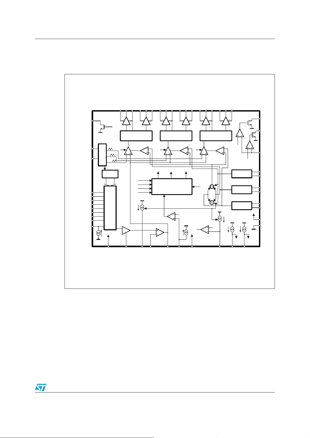
L6713A Block diagram
1 Block diagram
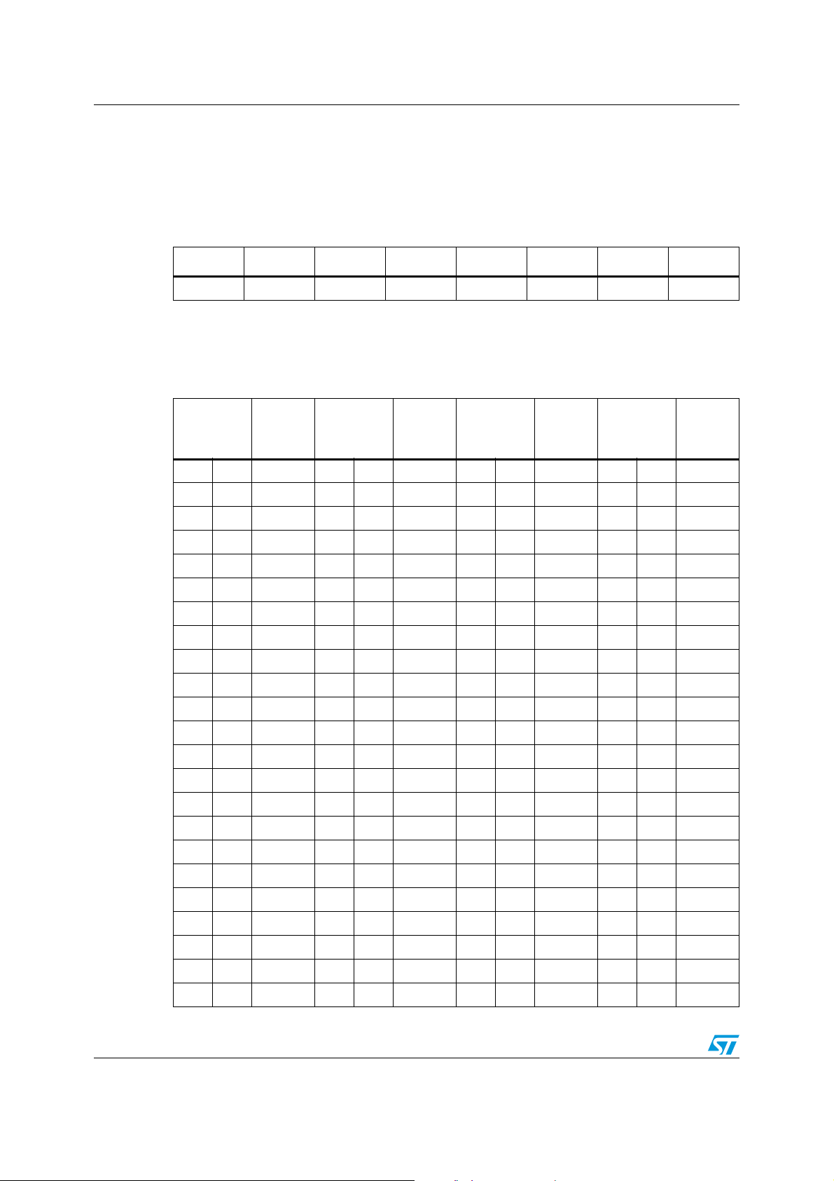
Figure 1. Block diagram
BOOT1
UGATE1
PHASE1
VCCDR1
LGATE1
PGND1
BOOT2
UGATE2
PHASE2
VCCDR2
LGATE2
PGND2
BOOT3
UGATE3
PHASE3
VCCDR3
LGATE3
PGND3
SS_END / PGOOD
OSC / FAULT
SS/ LTBG/ AMD
VID0
VID1
VID2
VID3
VID4
VID5
VID6
VID7 / D-VID
VID_SEL
2/3 PHASE
OSCILLATOR
DIGITAL
SOFT START
DAC
12.5μA
OUTEN
HS1 LS1 HS2 LS2 HS3 LS3
VID CONTROL
WITH DYNAMIC
OUTEN
LOGIC PWM
ADAPTIVE ANTI
CROSS CONDUCTION
CURRENT SHARING
CORRECTION
PWM1 PWM2 PWM3
VCC
VCCDR
OUTEN
SSOSC/AMD
DROOP
I
VREF
GND DROP
RECOVERY
FBG
ERROR
AMPLIFIER
FB
DROOP
LOGIC PWM
ADAPTIVE ANTI
CROSS CONDUCTION
CURRENT SHARING
CORRECTION
LTBLTB LTB
PWM1
L6713A
CONTROL LOGIC
AND PROTECTIONS
PWM3
PWM2
TOTAL DELIVERED CURRENT
+175mV / 1.800V / OVP
OVP
COMPARATOR
OFFSET
I
VSEN
COMP
TO OCP
LTB
LTB
OCP
COMPARATOR
LOGIC PWM
ADAPTIVE ANTI
CROSS CONDUCTION
CURRENT SHARING
CORRECTION
AVERAGE
CURRENT
+.1240V
OCP
OCSET
I
OCSET
12.5μA
3.600V
CH1 CURRENT
READING
CH2 CURRENT
READING
CH3 CURRENT
READING
12.5μA
OVP
OVP
3.200V
VCC
PHASE_SEL
PHASE _SEL
VR_HOT
VR_FAN
TM
CS1CS1+
CS2CS2+
CS3CS3+
VCC
SGND
5/64
Pin settings L6713A
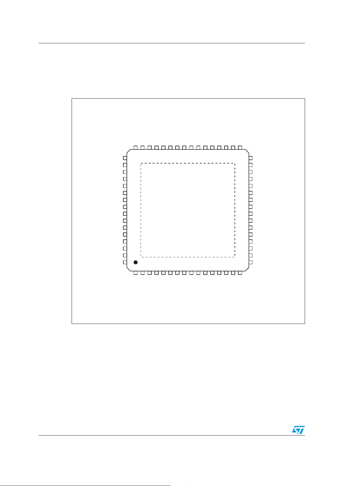
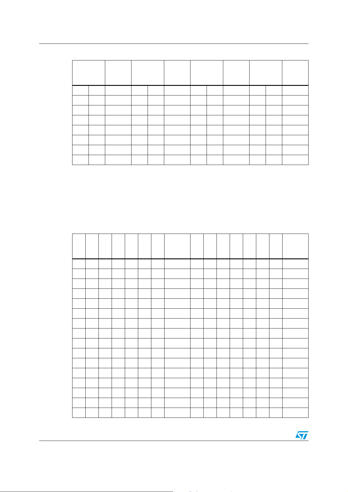
2 Pin settings
2.1 Pin connection
Figure 2. Pin connection (top view)
VID4
VID5
VID6
VID7 / D-VID
VR_FAN
VR_HOT
SS_END / PGOOD
VID0
VID1
VID2
VID3
FBG
VID_SEL
OCSET
OVP
OSC / FAULT
TM
SGND
N.C.
N.C.
N.C.
PGND2
LGATE2
VCCDR2
VCCDR3
LGATE3
PGND3
PGND1
LGATE1
VCCDR1
PHASE1
N.C.
48 47 46 45 44 43 42 41 40 39 38 37
49
50
51
52
53
54
55
56
57
58
59
60
61
62
63
64
123 45678 9 101112
N.C.
BOOT1
UAGTE1
UGATE3
PHASE3
L6713A
N.C.
BOOT3
PHASE2
UGATE2
BOOT2
36 35 34 33
13 14 15 16
N.C.
N.C.
32
SS / LTBG / AMD
31
CS1-
30
CS1+
29
CS3-
28
CS3+
27
CS2-
26
CS2+
25
N.C.
24
N.C.
23
COMP
22
FB
21
DROOP
20
VSEN
19
SGND
18
LT B
17
OUTEN
N.C.
N.C.
VCC
PHASE_SEL
6/64
L6713A Pin settings
2.2 Pin description
Table 2. Pin description
N° Pin Function
1UGATE1
2BOOT1
3 N.C. Not internally connected.
4 PHASE3
5UGATE3
6BOOT3
7 N.C. Not internally connected.
8 PHASE2
9UGATE2
10 BOOT2
11 N.C. Not internally connected.
12 N.C. Not internally connected.
Channel 1 HS driver output.
A small series resistors helps in reducing device-dissipated power.
Channel 1 HS driver supply.
Connect through a capacitor (100 nF typ.) to PHASE1 and provide necessary
Bootstrap diode. A small resistor in series to the boot diode helps in reducing
Boot capacitor overcharge.
Channel 3 HS driver return path.
It must be connected to the HS3 MOSFET source and provides return path for
the HS driver of channel 3.
Channel 3 HS driver output.
A small series resistors helps in reducing device-dissipated power.
Channel 3 HS driver supply.
Connect through a capacitor (100 nF typ.) to PHASE3 and provide necessary
Bootstrap diode. A small resistor in series to the boot diode helps in reducing
Boot capacitor overcharge.
Channel 2 HS driver return path.
It must be connected to the HS2 MOSFET source and provides return path for
the HS driver of channel 2. Leave floating when using 2 phase operation.
Channel 2 HS driver output.
A small series resistors helps in reducing device-dissipated power.
Leave floating when using 2 phase operation.
Channel 2 HS driver supply.
Connect through a capacitor (100 nF typ.) to PHASE2 and provide necessary
Bootstrap diode. A small resistor in series to the boot diode helps in reducing
Boot capacitor overcharge.Leave floating when using 2 phase operation.
13 N.C. Not internally connected.
14 N.C. Not internally connected.
15 VCC
PHASE_
16
SEL
Device supply voltage. The operative voltage is 12 V ±15 %. Filter with 1 µF
(typ) MLCC vs. SGND.
Phase selection pin. Internally pulled up by 12.5 µA(typ) to 5 V.
It allows selecting between 2 phase and 3 phase operation. See Table 11 for
details.
7/64

Pin settings L6713A
Table 2. Pin description (continued)
N° Pin Function
Output enable pin. Internally pulled up by 12.5 µA(typ) to 5 V.
Forced low, the device stops operations with all MOSFETs OFF: all the
17 OUTEN
18 LTB
19 SGND
20 VSEN
protections are disabled except for Preliminary over voltage.
Leave floating, the device starts-up implementing soft-start up to the selected
VID code.
Cycle this pin to recover latch from protections; filter with 1 nF (typ) vs. SGND.
Load transient boost pin.
- C
Internally fixed at 1 V, connecting a R
LTB
vs. VOUT allows to enable the
LTB
Load transient boost technology™: as soon as the device detects a transient
load it turns on all the PHASEs at the same time. Short to SGND to disable the
function.
All the internal references are referred to this pin. Connect to the PCB Signal
Ground.
It manages OVP and UVP protections and PGOOD (when applicable).
See “Output voltage monitor and protections” Section.
100 µA constant current
(I
generate a positive offset in according to the R
, See Table 5) is sunk by VSEN pin in order to
OFFSET
resistor between VSEN
OFFSET
pin and VOUT. See “Offset (Optional)” Section for details.
A current proportional to the total current read is sourced from this pin
according to the current reading gain.
21 DROOP
Short to FB to implement droop function or short to SGND to disable the
function. Connecting to SGND through a resistor and filtering with a capacitor,
the current info can be used for other purposes.
22 FB
23 COMP
Error amplifier inverting input. Connect with a resistor R
an RF - CF vs. COMP.
Error amplifier output. Connect with an R
The device cannot be disabled by pulling down this pin.
24 N.C. Not internally connected.
25 N.C. Not internally connected.
Channel 2 current sense positive input.
26 CS2+
Connect through an R-C filter to the phase-side of the channel 2 inductor.
Short to SGND or to V
OUT
See “Layout guidelines” Section for proper layout of this connection.
Channel 2 current sense negative input.
27 CS2-
Connect through a Rg resistor to the output-side of the channel 2 inductor.
Leave floating when using 2 Phase operation.
See “Layout guidelines” Section for proper layout of this connection.
Channel 3 current sense positive input.
28 CS3+
Connect through an R-C filter to the phase-side of the channel 3 inductor.
See “Layout guidelines” Section for proper layout of this connection.
Channel 3 current sense negative input.
29 CS3-
Connect through a Rg resistor to the output-side of the channel 3 inductor.
See “Layout guidelines” Section for proper layout of this connection.
FB
- CF vs. FB.
F
when using 2 Phase operation.
vs. VSEN and with
8/64

L6713A Pin settings
Table 2. Pin description (continued)
N° Pin Function
Channel 1 current sense positive input.
30 CS1+
31 CS1-
SS/ LTBG/
32
AMD
33 OVP
Connect through an R-C filter to the phase-side of the channel 1 inductor.
See “Layout guidelines” Section for proper layout of this connection.
Channel 1 current sense negative input.
Connect through a Rg resistor to the output-side of the channel 1 inductor.
See “Layout guidelines” Section for proper layout of this connection.
Soft-start oscillator, LTB gain and AMD selection pin.
It allows selecting between INTEL DACs and AMD DAC.
Short to SGND to select AMD DAC otherwise INTEL mode is selected.
When INTEL mode is selected trough this pin it is possible to select the soft-
start time and also the gain of LTB Technology™. See “Soft-start” Section” and
See “Load transient boost technologyTM” Section for details.
Over voltage programming pin. Internally pulled up by 12.5 µA (typ) to 5 V.
Leave floating to use built-in protection thresholds as reported into Ta b l e 1 2 .
Connect to SGND through a R
the OVP threshold to a fixed voltage according to the R
resistor and filter with 100 pF (max) to set
OVP
OVP
resistor.
See “Over voltage and programmable OVP” Section Section for details.
34 VID_SEL
35 OCSET
36 FBG
37
OSC/
FAULT
38 VID7/DVID
39 VID6
Intel mode. Internally pulled up by 12.5 µA (typ) to 5 V.
It allows selecting between VR10 (short to SGND, Ta bl e 8 ) or VR11 (floating,
See Table 7) DACs. See “Configuring the device” Section for details.
AMD mode. Not applicable. Needs to be shorted to SGND.
Over current set pin.
Connect to SGND through a R
also a C
capacitor to set a delay for the OCP intervention.
OCSET
resistor to set the OCP threshold. Connect
OCSET
See “Over current protection” Section for details.
Connect to the negative side of the load to perform remote sense.
See “Layout guidelines” Section for proper layout of this connection.
Oscillator pin.
It allows programming the switching frequency F
of each channel: the
SW
equivalent switching frequency at the load side results in being multiplied by the
phase number N.
Frequency is programmed according to the resistor connected from the pin vs.
SGND or VCC with a gain of 8 kHz/µA (see relevant section for details).
Leaving the pin floating programs a switching frequency of 200kHz per phase.
The pin is forced high (5 V) to signal an OVP FAULT: to recover from this
condition, cycle VCC or the OUTEN pin. See “Oscillator” Section for details.
VID7 - Intel mode. See VID5 to VID0 section.
DVID - AMD mode. DVID output.
CMOS output pulled high when the controller is performing a D-VID transition
(with 32 clock cycle delay after the transition has finished). See “Dynamic VID
transitions” Section Section for details.
Intel mode. See VID5 to VID0 section.
AMD mode. Not applicable. Needs to be shorted to SGND.
9/64

Pin settings L6713A
Table 2. Pin description (continued)
N° Pin Function
Intel mode. Voltage identification pins (also applies to VID6, VID7).
Internally pulled up by 25 µA to 5 V, connect to SGND to program a '0' or leave
floating to program a '1'.
They allow programming output voltage as specified in Tab l e 7 and Tab l e 8
according to VID_SEL status. OVP and UVP protection comes as a
40 to 45VID5 to
VID0
SS_END/
46
PGOOD
consequence of the programmed code (See Table 12).
AMD mode. Voltage identification pins.
Internally pulled down by 12.5 µA, leave floating to program a '0' while pull up to
more than 1.4 V to program a '1'.
They allow programming the output voltage as specified in Ta bl e 1 0 (VID7
doesn’t care). OVP and UVP protection comes as a consequence of the
programmed code (See Table 12).
Note. VID6 not used, need to be shorted to SGND.
SSEND - Intel mode. soft-start end signal.
Open drain output sets free after SS has finished and pulled low when
triggering any protection. Pull up to a voltage lower than 5 V (typ), if not used it
can be left floating.
PGOOD - AMD mode.
Open drain output set free after SS has finished and pulled low when VSEN is
lower than the relative threshold. Pull up to a voltage lower than 5 V (typ), if not
used it can be left floating.
Voltage regulator hot. Over temperature alarm signal.
47 VR_HOT
Open drain output, set free when TM overcomes the alarm threshold.
Thermal monitoring output enabled if Vcc > UVLO
See “Thermal monitor” Section for details and typical connections.
Voltage regulator fan. Over temperature warning signal.
48 VR_FAN
Open drain output, set free when TM overcomes the warning threshold.
Thermal monitoring output enabled if Vcc > UVLO
See “Thermal monitor” Section for details and typical connections.
Thermal monitor input.
49 TM
It senses the regulator temperature through apposite network and drives
VR_FAN and VR_HOT accordingly. Short TM pin to SGND if not used.
See “Thermal monitor” Section for details and typical connections.
50 SGND
All the internal references are referred to this pin. Connect to the PCB signal
Ground.
51 N.C. Not internally connected.
52 N.C. Not internally connected.
53 N.C. Not internally connected.
Channel 2 LS driver return path. Connect to power ground plane.
54 PGND2
It must be connected to power ground plane also when using 2-phase
operation.
Channel 2 LS driver output. A small series resistor helps in reducing device-
55 LGATE2
dissipated power.
Leave floating when using 2 phase operation.
VCC.
VCC.
10/64

L6713A Pin settings
Table 2. Pin description (continued)
N° Pin Function
Channel 2 LS driver supply.
It must be connected to others VCCDRx pins also when using 2-phase
56 VCCDR2
57 VCCDR3
operation.
LS driver supply can range from 5 Vbus up to 12 Vbus, filter with 1 µF MLCC
cap vs. PGND2.
Channel 3 LS driver supply.
It must be connected to others VCCDRx pins.
LS driver supply can range from 5 Vbus up to 12 Vbus, filter with 1 µF MLCC
cap vs. PGND3.
58 LGATE3
59 PGND3 Channel 3 LS driver return path. Connect to power ground plane.
60 PGND1 Channel 1 LS driver return path. Connect to power ground plane.
61 LGATE1
62 VCCDR1
63 PHASE1
64 N.C. Not internally connected.
PA D
Thermal
pad
Channel 3 LS driver output. A small series resistor helps in reducing devicedissipated power.
Channel 1 LS driver output. A small series resistor helps in reducing devicedissipated power.
Channel 1 LS driver supply.
It must be connected to others VCCDRx pins.
LS driver supply can range from 5 Vbus up to 12 Vbus, filter with 1 µF MLCC
cap vs. PGND1.
Channel 1 HS driver return path.
It must be connected to the HS1 MOSFET source and provides return path for
the HS driver of channel 1.
Thermal pad connects the silicon substrate and makes good thermal contact
with the PCB to dissipate the power necessary to drive the external MOSFETs.
Connect to the PGND plane with several VIAs to improve thermal conductivity.
11/64
Electrical data L6713A
3 Electrical data
3.1 Maximum ratings
Table 3. Absolute maximum ratings
Symbol Parameter Value Unit
V
V
BOOTx
V
UGATEx
V
, V
CC
- V
CC
V
PHASEx
CCDRx
- V
- V
BOOTx
PHASEx
PHASEx
to PGNDx 15 V
Boot voltage 15 V
15 V
7.5 V
LGATEx, PHASEx, to PGNDx -0.3 to V
+ 0.3 V
CC
VID0 to VID7, VID_SEL -0.3 to 5 V
All other pins to PGNDx -0.3 to 7 V
Static condition to PGNDx,
VCC = 14 V, BOOTx = 7 V,
-7.5 V
PHASEx = -7.5 V
Positive peak voltage to PGNDx;
T < 20 ns @ 600 kHz
26 V
3.2 Thermal data
Table 4. Thermal data
Symbol Parameter Value Unit
R
T
T
P
MAX
STG
T
Thermal resistance junction to ambient
thJA
(Device soldered on 2s2p PC board)
Maximum junction temperature 150 °C
Storage temperature range -40 to 150 °C
Junction temperature range 0 to 125 °C
J
Maximum power dissipation at TA = 25 °C 2.5 W
TOT
40 °C/W
12/64
L6713A Electrical characteristics
4 Electrical characteristics
V
= 12 V ± 15 %, TJ = 0 °C to 70 °C, unless otherwise specified
CC
Table 5. Electrical characteristics
Symbol Parameter Test condition Min. Typ. Max. Unit
Supply current
I
CC
I
CCDRx
I
BOOTx
VCC supply current
VCCDRx supply current LGATEx = OPEN; VCCDRx = 12 V 1 mA
BOOTx supply current
Power-ON
VCC turn-ON VCC Rising; VCCDRx = 5 V 8.9 9.3 V
UVLO
VCC
VCC turn-OFF VCC Falling; VCCDRx = 5 V 7.3 7.7 V
VCCDR turn-ON VCCDRx Rising; VCC = 12 V 4.5 4.8 V
UVLO
VCCDR
VCCDR turn-OFF VCCDRx Falling; VCC = 12 V 3.9 4.3 V
Pre-OVP turn-ON VCC Rising; VCCDRx = 5 V 3.6 4.2 V
UVLO
OVP
Pre-OVP turn-OFF VCC Falling; VCCDRx = 5 V 3.05 3.3 V
Oscillator and inhibit
F
OSC
T
1
T
2
T
3
Main oscillator accuracy
SS delay time Intel mode 1 ms
SS time T2 Intel mode; R
SS time T3 Intel mode 50 μs
Output enable intel mode
HGATEx and LGATEx = OPEN
VCCDRx = BOOTx = 12 V
HGATEx = OPEN; PHASEx to
PGNDx VCC = BOOTx = 12 V
OSC = OPEN
OSC = OPEN; T
= 0 °C to 125 °C
J
= 25 kΩ 500 μs
SSOSC
180
175
17 mA
0.75 mA
200 220
225
kHz
Rising thresholds voltage 0.80 0.85 0.90 V
Hysteresis 100 mV
OUTEN
Input low 0.80 V
Output enable AMD mode
Input high 1.40 V
OUTEN pull-up current OUTEN to SGND 12.5 μA
ΔV
OSC
PWMx ramp amplitude 3 V
FAULT Voltage at pin OSC OVP active 5 V
13/64
Electrical characteristics L6713A
Table 5. Electrical characteristics (continued)
Symbol Parameter Test condition Min. Typ. Max. Unit
Reference and DAC
Intel mode
VID = 1.000 V to VID = 1.600 V
FB = VOUT; FBG = GNDOUT
k
VID
Output voltage accuracy
AMD mode
VID = 1.000 V to VID = 1.550 V
FB = VOUT; FBG = GNDOUT
-0.5 - 0.5 %
-0.6 - 0.6 %
V
BOOT
Boot voltage Intel mode 1.081 V
VID pull-up current Intel mode; VIDx to SGND 25 μA
I
VID
VID
VID pull-down current AMD mode; VIDx to 5.4 V 12.5 μA
Intel mode; Input low
IL
AMD mode; Input low
0.3
0.8
VID thresholds
VID
IH
VID_SEL
VID_SEL threshold
(Intel mode)
Intel mode; Input high
AMD mode; Input high
Input low
Input high 0.8
0.8
1.35
0.3
VID_SEL pull-up current VIDSEL to SGND 12.5 μA
Error amplifier
A
0
EA DC gain 80 dB
SR EA slew rate COMP = 10 pF to SGND 20 V/μs
Differential current sensing and offset
I
CSx+
I
INFOxIAVG
--------------------------------- ---------
I
AVG
V
OCTH
Bias current Inductor sense 0 μA
–
Current sense mismatch Rg = 1 kΩ; I
Over current threshold V
(OCP) 1.215 1.240 1.265 V
OCSET
= 25 μA-3-3%
INFOx
Rg = 1 kΩ
K
IOCSET
k
IDROOP
I
OFFSET
OCSET current accuracy
Droop current deviation from
nominal value
2-PHASE, I
3-PHASE, I
Rg = 1kΩ
2-PHASE, I
3-PHASE, I
OCSET
OCSET
DROOP
DROOP
= 60 μA;
= 90 μA;
= 0 to 40 μA;
= 0 to 60 μA;
-5 - 5 %
-1 - 1 μA
Offset current VSEN = 0.500 V to 1.600 V 90 100 110 μA
Gate driver
V
V
V
t
RISE_UGATEx
I
UGATEx
R
UGATEx
HS rise time
HS source current BOOTx - PHASEx = 10 V 2 A
HS sink resistance BOOTx - PHASEx = 12 V 1.5 2 2.5 Ω
BOOTx - PHASEx = 10 V;
C
to PHASEx = 3.3 nF
UGATEx
14/64
15 30 ns
L6713A Electrical characteristics
Table 5. Electrical characteristics (continued)
Symbol Parameter Test condition Min. Typ. Max. Unit
t
RISE_LGATEx
I
LGATEx
R
LGATEx
LS rise time
LS source current VCCDRx = 10 V 1.8 A
LS sink resistance VCCDRx = 12 V 0.7 1.1 1.5 Ω
VCCDRx = 10 V;
C
to PGNDx = 5.6 nF
LGATEx
30 55 ns
Protections
1.300 V
OVP
Over voltage protection
(VSEN rising)
Intel mode; Before V
BOOT
Intel mode; Above VID 150 175 200 mV
AMD mode 1.700 1.740 1.780 V
current OVP = SGND 11.5 12.5 13.5 μA
I
Program-
mable OVP
Pre-OVP
OVP
Comparator offset voltage OVP = 1.8 V -20 0 20 mV
Preliminary over voltage
protection
UVLO
VCC > UVLO
SGND
< VCC < UVLO
OVP
VCC
VCC
& OUTEN =
1.800 V
Hysteresis 350 mV
UVP Under voltage protection VSEN falling; Below VID -750 mV
PGOOD PGOOD threshold
V
SSEND/
PGOOD
SSEND / PGOOD
voltage low
AMD mode;
VSEN falling; Below VID
I = -4 mA 0.4 V
-300
mV
Thermal monitor
TM warning (VR_FAN) V
V
TM
TM alarm (VR_HOT) V
TM hysteresis 100 mV
V
VR_HOT
V
VR_FAN
VR_HOT voltage low;
;
VR_FAN voltage low
rising 3.2 V
TM
rising 3.420 3.6 3.770 V
TM
I = -4 mA
0.4
0.4
V
V
15/64
VID Tables L6713A
5 VID Tables
5.1 Mapping for the Intel VR11 mode
Table 6. Voltage identification (VID) mapping for Intel VR11 mode
VID7 VID6 VID5 VID4 VID3 VID2 VID1 VID0
800 mV 400 mV 200 mV 100 mV 50 mV 25 mV 12.5 mV 6.25 mV
5.2 Voltage identification (VID) for Intel VR11 mode
Table 7. Voltage identification (VID) for Intel VR11 mode (See Note)
Output
HEX code
0 0 OFF 4 0 1.21250 8 0 0.81250 C 0 0.41250
0 1 OFF 4 1 1.20625 8 1 0.80625 C 1 0.40625
0 2 1.60000 4 2 1.20000 8 2 0.80000 C 2 0.40000
0 3 1.59375 4 3 1.19375 8 3 0.79375 C 3 0.39375
0 4 1.58750 4 4 1.18750 8 4 0.78750 C 4 0.38750
0 5 1.58125 4 5 1.18125 8 5 0.78125 C 5 0.38125
0 6 1.57500 4 6 1.17500 8 6 0.77500 C 6 0.37500
0 7 1.56875 4 7 1.16875 8 7 0.76875 C 7 0.36875
0 8 1.56250 4 8 1.16250 8 8 0.76250 C 8 0.36250
0 9 1.55625 4 9 1.15625 8 9 0.75625 C 9 0.35625
0 A 1.55000 4 A 1.15000 8 A 0.75000 C A 0.35000
0 B 1.54375 4 B 1.14375 8 B 0.74375 C B 0.34375
0 C 1.53750 4 C 1.13750 8 C 0.73750 C C 0.33750
0 D 1.53125 4 D 1.13125 8 D 0.73125 C D 0.33125
0 E 1.52500 4 E 1.12500 8 E 0.72500 C E 0.32500
0 F 1.51875 4 F 1.11875 8 F 0.71875 C F 0.31875
1 0 1.51250 5 0 1.11250 9 0 0.71250 D 0 0.31250
voltage
(1)
HEX code
Output
voltage
(1)
HEX code
Output
voltage
(1)
HEX code
Output
voltage
(1)
1 1 1.50625 5 1 1.10625 9 1 0.70625 D 1 0.30625
1 2 1.50000 5 2 1.10000 9 2 0.70000 D 2 0.30000
1 3 1.49375 5 3 1.09375 9 3 0.69375 D 3 0.29375
1 4 1.48750 5 4 1.08750 9 4 0.68750 D 4 0.28750
1 5 1.48125 5 5 1.08125 9 5 0.68125 D 5 0.28125
1 6 1.47500 5 6 1.07500 9 6 0.67500 D 6 0.27500
16/64

L6713A VID Tables
Table 7. Voltage identification (VID) for Intel VR11 mode (See Note) (continued)
HEX code
Output
voltage
(1)
HEX code
Output
voltage
(1)
HEX code
Output
voltage
(1)
HEX code
Output
voltage
(1)
1 7 1.46875 5 7 1.06875 9 7 0.66875 D 7 0.26875
1 8 1.46250 5 8 1.06250 9 8 0.66250 D 8 0.26250
1 9 1.45625 5 9 1.05625 9 9 0.65625 D 9 0.25625
1 A 1.45000 5 A 1.05000 9 A 0.65000 D A 0.25000
1 B 1.44375 5 B 1.04375 9 B 0.64375 D B 0.24375
1 C 1.43750 5 C 1.03750 9 C 0.63750 D C 0.23750
1 D 1.43125 5 D 1.03125 9 D 0.63125 D D 0.23125
1 E 1.42500 5 E 1.02500 9 E 0.62500 D E 0.22500
1 F 1.41875 5 F 1.01875 9 F 0.61875 D F 0.21875
2 0 1.41250 6 0 1.01250 A 0 0.61250 E 0 0.21250
2 1 1.40625 6 1 1.00625 A 1 0.60625 E 1 0.20625
2 2 1.40000 6 2 1.00000 A 2 0.60000 E 2 0.20000
2 3 1.39375 6 3 0.99375 A 3 0.59375 E 3 0.19375
2 4 1.38750 6 4 0.98750 A 4 0.58750 E 4 0.18750
2 5 1.38125 6 5 0.98125 A 5 0.58125 E 5 0.18125
2 6 1.37500 6 6 0.97500 A 6 0.57500 E 6 0.17500
2 7 1.36875 6 7 0.96875 A 7 0.56875 E 7 0.16875
2 8 1.36250 6 8 0.96250 A 8 0.56250 E 8 0.16250
2 9 1.35625 6 9 0.95625 A 9 0.55625 E 9 0.15625
2 A 1.35000 6 A 0.95000 A A 0.55000 E A 0.15000
2 B 1.34375 6 B 0.94375 A B 0.54375 E B 0.14375
2 C 1.33750 6 C 0.93750 A C 0.53750 E C 0.13750
2 D 1.33125 6 D 0.93125 A D 0.53125 E D 0.13125
2 E 1.32500 6 E 0.92500 A E 0.52500 E E 0.12500
2 F 1.31875 6 F 0.91875 A F 0.51875 E F 0.11875
3 0 1.31250 7 0 0.91250 B 0 0.51250 F 0 0.11250
3 1 1.30625 7 1 0.90625 B 1 0.50625 F 1 0.10625
3 2 1.30000 7 2 0.90000 B 2 0.50000 F 2 0.10000
3 3 1.29375 7 3 0.89375 B 3 0.49375 F 3 0.09375
3 4 1.28750 7 4 0.88750 B 4 0.48750 F 4 0.08750
3 5 1.28125 7 5 0.88125 B 5 0.48125 F 5 0.08125
3 6 1.27500 7 6 0.87500 B 6 0.47500 F 6 0.07500
3 7 1.26875 7 7 0.86875 B 7 0.46875 F 7 0.06875
17/64
VID Tables L6713A
Table 7. Voltage identification (VID) for Intel VR11 mode (See Note) (continued)
HEX code
Output
voltage
(1)
HEX code
Output
voltage
(1)
HEX code
Output
voltage
(1)
HEX code
Output
voltage
(1)
3 8 1.26250 7 8 0.86250 B 8 0.46250 F 8 0.06250
3 9 1.25625 7 9 0.85625 B 9 0.45625 F 9 0.05625
3 A 1.25000 7 A 0.85000 B A 0.45000 F A 0.05000
3 B 1.24375 7 B 0.84375 B B 0.44375 F B 0.04375
3 C 1.23750 7 C 0.83750 B C 0.43750 F C 0.03750
3 D 1.23125 7 D 0.83125 B D 0.43125 F D 0.03125
3 E 1.22500 7 E 0.82500 B E 0.42500 F E OFF
3 F 1.21875 7 F 0.81875 B F 0.41875 F F OFF
1. According to VR11 specs, the device automatically regulates output voltage 19 mV lower to avoid any
external offset to modify the built-in 0.5 % accuracy improving TOB performances. Output regulated
voltage is than what extracted from the table lowered by 19 mV built-in offset.
5.3 Voltage identifications (VID) for Intel VR10 mode + 6.25 mV
(VID7 does not care)
Table 8. Voltage identifications (VID) for Intel VR10 mode + 6.25 mV (See Note)
VID4VID3VID2VID1VID0VID5VID
6
Output
voltage
(1)
VID4VID3VID2VID1VID0VID5VID
6
Output
voltage
(1)
01010111.60000 11010111.20000
01010101.59375 11010101.19375
01011011.58750 11011011.18750
01011001.58125 11011001.18125
01011111.57500 11011111.17500
01011101.56875 11011101.16875
01100011.56250 11100011.16250
01100001.55625 11100001.15625
01100111.55000 11100111.15000
01100101.54375 11100101.14375
01101011.53750 11101011.13750
01101001.53125 11101001.13125
01101111.52500 11101111.12500
01101101.51875 11101101.11875
01110011.51250 11110011.11250
01110001.50625 11110001.10625
18/64

L6713A VID Tables
Table 8. Voltage identifications (VID) for Intel VR10 mode + 6.25 mV (See Note)
VID4VID3VID2VID1VID0VID5VID
6
Output
voltage
(1)
VID4VID3VID2VID1VID0VID5VID
6
Output
voltage
(1)
01110111.50000 11110111.10000
01110101.49375 11110101.09375
01111011.48750 1111101 OFF
01111001.48125 1111100 OFF
01111111.47500 1111111 OFF
01111101.46875 1111110 OFF
10000011.46250 00000011.08750
10000001.45625 00000001.08125
10000111.45000 00000111.07500
10000101.44375 00000101.06875
10001011.43750 00001011.06250
10001001.43125 00001001.05625
10001111.42500 00001111.05000
10001101.41875 00001101.04375
10010011.41250 00010011.03750
10010001.40625 00010001.03125
10010111.40000 00010111.02500
10010101.39375 00010101.01875
10011011.38750 00011011.01250
10011001.38125 00011001.00625
10011111.37500 00011111.00000
10011101.36875 00011100.99375
10100011.36250 00100010.98750
10100001.35625 00100000.98125
10100111.35000 00100110.97500
10100101.34375 00100100.96875
10101011.33750 00101010.96250
10101001.33125 00101000.95625
10101111.32500 00101110.95000
10101101.31875 00101100.94375
10110011.31250 00110010.93750
10110001.30625 00110000.93125
10110111.30000 00110110.92500
19/64

VID Tables L6713A
Table 8. Voltage identifications (VID) for Intel VR10 mode + 6.25 mV (See Note)
6
Output
voltage
(1)
VID4VID3VID2VID1VID0VID5VID
VID4VID3VID2VID1VID0VID5VID
10110101.29375 00110100.91875
10111011.28750 00111010.91250
10111001.28125 00111000.90625
10111111.27500 00111110.90000
10111101.26875 00111100.89375
11000011.26250 01000010.88750
11000001.25625 01000000.88125
11000111.25000 01000110.87500
11000101.24375 01000100.86875
11001011.23750 01001010.86250
11001001.23125 01001000.85625
11001111.22500 01001110.85000
11001101.21875 01001100.84375
11010011.21250 01010010.83750
11010001.20625 01010000.83125
1. According to VR10.x specs, the device automatically regulates output voltage 19 mV lower to avoid any
external offset to modify the built-in 0.5 % accuracy improving TOB performances. Output regulated
voltage is than what extracted from the table lowered by 19mVbuilt-in offset. VID7 doesn’t care.
6
Output
voltage
(1)
5.4 Mapping for the AMD 6 bit mode
Table 9. Voltage identifications (VID) mapping for AMD 6 bit mode
VID4 VID3 VID2 VID1 VID0
400 mV 200 mV 100 mV 50 mV 25 mV
5.5 Voltage identifications (VID) codes for AMD 6 bit mode
Table 10. Voltage identifications (VID) codes for AMD 6 bit mode (See Note)
VID5 VID4 VID3 VID2 VID1 VID0
0000001.5500 1 000000.7625
0000011.5250 1 000010.7500
0000101.5000 1 000100.7375
0000111.4750 1 000110.7250
20/64
Output
voltage
VID5 VID4 VID3 VID2 VID1 VID0
(1)
Output
voltage
(1)

L6713A VID Tables
Table 10. Voltage identifications (VID) codes for AMD 6 bit mode (See Note) (continued)
VID5 VID4 VID3 VID2 VID1 VID0
Output
voltage
VID5 VID4 VID3 VID2 VID1 VID0
(1)
Output
voltage
(1)
0001001.4500 1 001000.7125
0001011.4250 1 001010.7000
0001101.4000 1 001100.6875
0001111.3750 1 001110.6750
0010001.3500 1 010000.6625
0010011.3250 1 010010.6500
0010101.3000 1 010100.6375
0010111.2750 1 010110.6250
0011001.2500 1 011000.6125
0011011.2250 1 011010.6000
0011101.2000 1 011100.5875
0011111.1750 1 011110.5750
0100001.1500 1 100000.5625
0100011.1250 1 100010.5500
0100101.1000 1 100100.5375
0100111.0750 1 100110.5250
0101001.0500 1 101000.5125
0101011.0250 1 101010.5000
0101101.0000 1 101100.4875
0101110.9750 1 101110.4750
0110000.9500 1 110000.4625
0110010.9250 1 110010.4500
0110100.9000 1 110100.4375
0110110.8750 1 110110.4250
0111000.8500 1 111000.4125
0111010.8250 1 111010.4000
0111100.8000 1 111100.3875
0111110.7750 1 111110.3750
1. VID6 not applicable, need to be left unconnected.
21/64

Reference schematic L6713A
6 Reference schematic
Figure 3. Reference schematic - Intel VR10.x, VR11 - 3-phase operation
VIN
GNDIN
to SSEND
VID bus from CPU
VID_SEL
OUTEN
CLTB
RLTB
CP
CI
RI
L6713A REF.SCH:
Intel Mode - 3-Phase Operation
CF
RF
RSSOSC
RFB
ROFFSET
62
56
57
15
19,50
33
16
35
37
32
39
40
41
42
43
44
45
34
17
18
23
22
21
20
36
LIN
VCCDR1
VCCDR2
VCCDR3
VCC
SGND
OVP
PHASE_SEL
OCSET
OSC/FAULT
SS/LTBG/AMD
VID7 / DVID
VID6
VID5
VID4
VID3
VID2
VID1
VID0
VID_SEL
OUTEN
LTB
COMP
SS_END / PGOOD
FB
DROOP
VSEN
FBG
2
BOOT1
1
UGATE1
63,64
PHASE1
61
LGATE1
60
PGND1
31
30
10
7,8
55
54
27
26
3,4
58
59
29
28
46
47
49
Rg
9
Rg
6
5
Rg
CS1-
CS1+
BOOT2
UGATE2
PHASE2
LGATE2
PGND2
CS2-
CS2+
BOOT3
L6713A
UGATE3
PHASE3
LGATE3
PGND3
CS3-
CS3+
VR_HOT
VR_FAN 48
TM
RTM
VIN
HS1
LS1
VIN
HS2
LS2
VIN
HS3
LS3
NTC
+5V
to BOOT1
to BOOT2
COUT
to BOOT3
Vcc_core
LOAD
GND_core
SS_END
CIN
L1
R
C
L2
R
C
L3
R
C
22/64

L6713A Reference schematic
Figure 4. Reference schematic - Intel VR10.x, VR11 - 2-phase operation
V
GND
IN
IN
to SSEND
C
LTB
R
LTB
VID bus from CPU
VID_SEL
OUTEN
C
P
C
I
R
I
62
56
57
15
19,50
33
16
35
37
32
SSOSC
R
39
40
41
42
43
44
45
34
17
18
23
C
F
R
F
22
21
R
FB
20
R
OFFSET
36
L
VCCDR1
VCCDR2
VCCDR3
VCC
SGND
OVP
PHASE_SEL
OCSET
OSC/FAULT
SS/LTBG/AMD
VID7 / DVID
VID6
VID5
VID4
VID3
VID2
VID1
VID0
VID_SEL
OUTEN
LTB
COMP
SS_END / PGOOD
FB
DROOP
VSEN
FBG
IN
BOOT1
UGATE1
63,64
PHASE1
LGATE1
PGND1
CS1-
CS1+
BOOT2
UGATE2
7,8
PHASE2
LGATE2
PGND2
CS2-
CS2+
BOOT3
L6713A
UGATE3
3,4
PHASE3
LGATE3
PGND3
CS3-
CS3+
VR_HOT
VR_FAN 48
TM
2
1
61
60
31
Rg
30
10
9
55
54
27
26
Short to SGND (or to VOUT)
6
5
58
59
29
Rg
28
46
47
49
to BOOT1
to BOOT3
C
V
IN
IN
HS1
L1
LS1
R
C
Vcc_core
C
V
IN
OUT
LOAD
GND_core
HS3
L3
LS3
R
C
SS_END
+5V
NTC
R
TM
L6713A REF.SCH:
Intel Mode -2-Phase Operation
23/64

Reference schematic L6713A
Figure 5. Reference schematic - AMD 6 bit - 3-phase operation
V
GND
IN
IN
C
LTB
R
LTB
VID bus from CPU
OUTEN
C
C
P
R
C
I
R
I
62
56
57
15
19,50
33
16
35
37
32
38
39
40
41
42
43
44
45
34
17
18
23
F
F
22
21
R
FB
20
R
OFFSET
36
L
VCCDR1
VCCDR2
VCCDR3
VCC
SGND
OVP
PHASE_SEL
OCSET
OSC/FAULT
SS/LTBG/AMD
VID7 / DVID
VID6
VID5
VID4
VID3
VID2
VID1
VID0
VID_SEL
OUTEN
LTB
COMP
SS_END / PGOOD
FB
DROOP
VSEN
FBG
IN
BOOT1
UGATE1
63,64
PHASE1
LGATE1
PGND1
CS1-
CS1+
BOOT2
UGATE2
PHASE2
LGATE2
PGND2
CS2-
CS2+
BOOT3
L6713A
UGATE3
PHASE3
LGATE3
PGND3
CS3-
CS3+
VR_HOT
VR_FAN 48
TM
61
60
31
30
10
7,8
55
54
27
26
3,4
58
59
29
28
46
47
49
to BOOT1
to BOOT2
2
1
HS1
V
IN
C
IN
to BOOT3
L1
LS1
R
C
Rg
V
IN
9
HS2
L2
LS2
R
C
Rg
Vcc_core
C
6
5
HS3
V
IN
OUT
LOAD
GND_core
L3
LS3
R
C
Rg
PGOOD
+5V
NTC
R
TM
L6713A REF.SCH:
AMD Mode - 3-Phase Operation
24/64

L6713A Reference schematic
Figure 6. Reference schematic - AMD 6 bit - 2-phase operation
V
GND
IN
IN
C
LTB
R
LTB
VID bus from CPU
OUTEN
C
C
P
R
C
I
R
I
62
56
57
15
19,50
33
16
35
37
32
38
39
40
41
42
43
44
45
34
17
18
23
F
F
22
21
R
FB
20
R
OFFSET
36
L
VCCDR1
VCCDR2
VCCDR3
VCC
SGND
OVP
PHASE_SEL
OCSET
OSC/FAULT
SS/LTBG/AMD
VID7 / DVID
VID6
VID5
VID4
VID3
VID2
VID1
VID0
VID_SEL
OUTEN
LTB
COMP
SS_END / PGOOD
FB
DROOP
VSEN
FBG
IN
BOOT1
UGATE1
63,64
PHASE1
LGATE1
PGND1
CS1-
CS1+
BOOT2
UGATE2
PHASE2
LGATE2
PGND2
CS2-
CS2+
BOOT3
L6713A
UGATE3
PHASE3
LGATE3
PGND3
CS3-
CS3+
VR_HOT
VR_FAN 48
TM
2
1
61
60
31
Rg
30
10
9
7,8
55
54
27
26
Short to SGND (or to VOUT)
6
5
3,4
58
59
29
Rg
28
46
47
49
to BOOT1
to BOOT3
C
V
IN
IN
HS1
L1
LS1
R
C
Vcc_core
C
V
IN
OUT
LOAD
GND_core
HS3
L3
LS3
R
C
PGOOD
+5V
NTC
R
TM
L6713A REF.SCH:
AMD Mode - 2-Phase Operation
25/64

Device description L6713A
7 Device description
L6713A is two/three phase PWM controller with embedded high current drivers providing
complete control logic and protections for a high performance step-down DC-DC voltage
regulator optimized for advanced microprocessor power supply.
Multi phase buck is the simplest and most cost-effective topology employable to satisfy the
increasing current demand of newer microprocessors and modern high current VRM
modules.
It allows distributing equally load and power between the phases using smaller, cheaper and
most common external power MOSFETs and inductors. Moreover, thanks to the equal
phase shift between each phase, the input and output capacitor count results in being
reduced. Phase interleaving causes in fact input RMS current and output ripple voltage
reduction and show an effective output switching frequency increase: the 200kHz freerunning frequency per phase, externally adjustable through a resistor, results multiplied on
the output by the number of phases.
L6713A is a dual-edge asynchronous PWM controller featuring load transient boost
LTB Technology™ (patent pending): the device turns on simultaneously all the phases as
soon as a load transient is detected allowing to minimize system cost by providing the
fastest response to load transition.
Load transition is detected (through LTB pin) measuring the derivate dV/dt of the output
voltage and the dV/dt can be easily programmed extending the system design flexibility.
Moreover, load transient boost LTB Technology™ gain can be easily modified in order to
keep under control the output voltage ring back.
LTB Technology™ can be disabled and in this condition the device works as a dual-edge
asynchronous PWM.
The controller allows to implement a scalable design: a three phase design can be easily
downgraded to two phase simply by leaving one phase not mounted and leaving
PHASE_SEL pin floating.
The same design can be used for more than one project saving development and debug
time. In the same manner, a two phase design can be further upgraded to three phase
facing with newer and highly-current-demanding applications.
L6713A permits easy system design by allowing current reading across inductor in fully
differential mode. Also a sense resistor in series to the inductor can be considered to
improve reading precision.
The current information read corrects the PWM output in order to equalize the average
current carried by each phase limiting the error to ±3 % over static and dynamic conditions
unless considering the sensing element spread.
The controller includes multiple DACs, selectable through an apposite pin, allowing
compatibility with both Intel VR10,VR11 and AMD 6BIT processors specifications, also
performing D-VID transitions accordingly.
Low-side-less start-up allows soft-start over pre-biased output avoiding dangerous current
return through the main inductors as well as negative spike at the load side.
26/64

L6713A Device description
L6713A provides a programmable over-voltage protection to protect the load from
dangerous over stress. It can be externally set to a fixed voltage through an apposite
resistor, or it can be set internally, latching immediately by turning ON the lower driver and
driving high the FAULT pin.
Furthermore, preliminary OVP protection also allows the device to protect load from
dangerous OVP when VCC is not above the UVLO threshold.
The over-current protection is on the total delivered current and causes the device turns
OFF all MOSFETs and latches the condition.
L6713A provides also system Thermal Monitoring: through an apposite pin the device
senses the temperature of the hottest component in the application driving the Warning and
the Alarm signal as a consequence.
A compact 10 x 10 mm body TQFP64 package with exposed thermal pad allows dissipating
the power to drive the external MOSFET through the system board.
27/64

Configuring the device L6713A
8 Configuring the device
Number of phases and multiple DACs need to be configured before the system starts-up by
programming the apposite pin PHASE_SEL and SS/LTBG/AMD pin.
The configuration of this pin identifies two main working areas (See Table 12) distinguishing
between compliancy with Intel VR10,VR11 or AMD 6BIT specifications. According to the
main specification considered, further customizations can be done: main differences are
regarding the DAC table, soft-start implementation, protection management and Dynamic
VID Transitions. See Table 13 and See Table 14 for further details about the device
configuration.
8.1 Number of phases selection
L6713A allows to select between two and three phase operation simply using the
PHASE_SEL pin, as shown in the following table.
Table 11. Number of phases setting
PHASE_SEL pin Number of phases Phases used
Floating 2-PHASE Phase1, Phase3
Short to SGND 3-PHASE Phase1, Phase2, Phase3
8.2 DAC selection
L6713A embeds a selectable DAC (through SS/LTBG/AMD pin, See Table 12) that allows to
regulate the output voltage with a tolerance of ±0.5% (±0.6% for AMD DAC) recovering from
offsets and manufacturing variations. In case of selecting Intel mode, the device
automatically introduces a -19 mV (both VRD10.x and VR11) offset to the regulated voltage
in order to avoid any external offset circuitry to worsen the guaranteed accuracy and, as a
consequence, the calculated system TOB.
Table 12. DAC settings (See note)
SS / LTBG / AMD
Resistor (R
vs. SGND
0 (Short) AMD
> 2.4 kΩ Intel
SSOSC
)
DAC Soft-start time LTB
Not
programmable
Programmable
trough R
SSOSC
(LTB
Programmable
trough R
(LTB™ gain ≤ 2)
™ gain OVP UVP
1.800 V (typ)
Fixed
™ gain = 2)
SSOSC
or
Programmable
VID + 175 mV
(typ)
or
programmable
-750 mV
-750 mV
(typ)
(typ)
Note: When selecting Intel mode, SS/LTBG/AMD pin is used to select both soft-start time and
LT B
™ gain (see dedicated sections).
28/64

L6713A Configuring the device
Output voltage is programmed through the VID pins: they are inputs of an internal DAC that
is realized by means of a series of resistors providing a partition of the internal voltage
reference. The VID code drives a multiplexer that selects a voltage on a precise point of the
divider. The DAC output is delivered to an amplifier obtaining the voltage reference (i.e. the
set-point of the error amplifier, V
REF
).
Table 13. Intel mode configuration (See Note)
Pin Function
(1)
Typical connection
SS / LTBG /
AMD
VID_SEL
VID7 to VID0
SSEND /
PGOOD
It allows programming the soft-start time T
and also the LTB Technology™ gain. See “Soft-
start” Section and See “Load transient boost
technologyTM” Section for details.
It allows selecting between VR11 DAC or
VR10.x + 6.25 mV extended DAC.
Static info, no dynamic changes allowed.
They allow programming the output voltage
according to Ta b le 7 and Ta bl e 8 .
Dynamic transitions managed, See “Dynamic
VID transitions” Section for details.
Soft-start end signal set free after soft-start has
finished. It only indicates soft-start has finished.
SS
R
signal diode vs. SSEND pin.
(LTB
Open: VR11 (
short to SGND: VR10.x
Ta bl e 8 ).
(
Open: Logic “1” (25 μA pull-up)
Short to SGND: “0”
Pull-up to anything lower
than 5 V.
resistor in series to
SSOSC
™ gain = 2, default value).
Ta bl e 7 ).
Note: VID pull-ups / pull-downs, VID voltage thresholds and OUTEN thresholds changes
according to the selected DAC: See Table 5 for details.
Table 14. AMD mode configuration (See Note)
Pin Function Typical connection
SS / LTBG /
AMD
VID_SEL Not applicable Need to be shorted to SGND.
VID7 / DVID
It allows programming AMD 6 BIT DAC. Short to SGND.
Pulled high when performing a D-VID transition.
The pin is kept high with a 32 clock cycles delay.
Not applicable
VID6 Not applicable Need to be shorted to SGND.
They allow programming the output voltage
VID5 to VID0
SSEND /
PGOOD
according to Ta bl e 1 0.
Dynamic transitions managed, See “Dynamic
VID transitions” Section for details.
Power good signal set free after soft-start has
finished whenever the output voltage is within
limits.
Open: “0” (12.5 μA pull-down)
Pull-up to V > 1.4 V: “1”
Pull-up to anything lower
than 5 V.
Note: VID pull-ups / pull-downs, VID voltage thresholds and OUTEN thresholds changes
according to the selected DAC: See Table 5 for details.
29/64

Power dissipation L6713A
9 Power dissipation
L6713A embeds high current MOSFET drivers for both high side and low side MOSFETs: it
is then important to consider the power the device is going to dissipate in driving them in
order to avoid overcoming the maximum junction operative temperature. In addition, since
the device has an exposed pad to better dissipate the power, the thermal resistance
between junction and ambient consequent to the layout is also important: thermal pad
needs to be soldered to the PCB ground plane through several VIAs in order to facilitate the
heat dissipation.
Two main terms contribute in the device power dissipation: bias power and drivers' power.
The first one (P
and it is simply quantifiable as follow (assuming to supply HS and LS drivers with the same
VCC of the device):
) depends on the static consumption of the device through the supply pins
DC
P
DC
V
CCICC
NI
⋅ NI
CCDRx
⋅++()⋅=
BOOTx
where N is the number of phases.
Drivers' power is the power needed by the driver to continuously switch on and off the
external MOSFETs; it is a function of the switching frequency and total gate charge of the
selected MOSFETs. It can be quantified considering that the total power P
dissipated to
SW
switch the MOSFETs (easy calculable) is dissipated by three main factors: external gate
resistance (when present), intrinsic MOSFET resistance and intrinsic driver resistance. This
last term is the important one to be determined to calculate the device power dissipation.
The total power dissipated to switch the MOSFETs results:
SW
NFSWQ
P
⋅ Q
GHSVBOOT
⋅+()⋅⋅=
GLSVCCDRx
External gate resistors helps the device to dissipate the switching power since the same
power P
will be shared between the internal driver impedance and the external resistor
SW
resulting in a general cooling of the device. When driving multiple MOSFETs in parallel, it is
suggested to use one gate resistor for each MOSFET.
30/64

L6713A Power dissipation
Figure 7. L6713A dissipated power (quiescent + switching)
4500
4000
3500
3000
2500
2000
1500
1000
500
Controller Dissipated Power [mW]
0
50 150 250 350 450 550 650 750 850 950 1050
2-PHASE Operation ; Rgate=0; Rmosfet=0
HS=1xSTD38NH02L; LS=1xSTD90NH02L
HS=2xSTD38NH02L; LS=2xSTD90NH02L
HS=1xSTD55NH2LL; LS=1xSTD95NH02L
HS=2xSTD55NH2LL; LS=2xSTD95NH02L
HS=3xSTD55NH22L; LS=3xSTD95NH02L
Switching frequen cy [kHz] per phase
7000
6000
5000
4000
3000
2000
1000
Controller Dissipated Power [mW]
0
50 150 250 350 450 550 650 750 850 950 1050
3-PHASE Operatio n; Rgate=0; Rmosfet=0
HS=1xSTD38NH02L; LS=1xSTD90NH02L
HS=2xSTD38NH02L; LS=2xSTD90NH02L
HS=1xSTD55NH2LL; LS=1xSTD95NH02L
HS=2xSTD55NH2LL; LS=2xSTD95NH02L
HS=3xSTD55NH22L; LS=3xSTD95NH02L
Switching frequen cy [kHz] per phase
4000
3500
3000
2500
2000
1500
1000
500
Contr oller Dis sipated Power [mW]
0
2-PHASE Operation ; Rhs=2.2; Rls=3. 3; Rmosfet=1
HS=1xSTD38NH02L; LS=1xSTD90NH02L
HS=2xSTD38NH02L; LS=2xSTD90NH02L
HS=1xSTD55NH2LL; LS=1xSTD95NH02L
HS=2xSTD55NH2LL; LS=2xSTD95NH02L
HS=3xSTD55NH22L; LS=3xSTD95NH02L
50 150 250 350 450 550 650 750 850 950 1050
Switchin g frequency [kHz] per phase
4000
3500
3000
2500
2000
1500
1000
500
Controller Dissipated Power [mW]
0
3-PHASE Operati on; Rhs=2 .2; Rls=3.3; Rmosfet =1
HS=1 xSTD38 NH02L; LS=1x STD90NH0 2L
HS=2 xSTD38 NH02L; LS=2x STD90NH0 2L
HS=1 xSTD55 NH2LL; LS=1x STD95NH0 2L
HS=2 xSTD55 NH2LL; LS=2x STD95NH0 2L
HS=3 xSTD55 NH22L; LS=3x STD95NH0 2L
50 15 0 250 350 450 550 650 750 850 950 1050
Switch ing frequency [kHz] per phase
31/64

Current reading and current sharing loop L6713A
10 Current reading and current sharing loop
L6713A embeds a flexible, fully-differential current sense circuitry that is able to read across
inductor parasitic resistance or across a sense resistor placed in series to the inductor
element. The fully-differential current reading rejects noise and allows placing sensing
element in different locations without affecting the measurement's accuracy.
Reading current across the inductor DCR, the current flowing trough each phase is read
using the voltage drop across the output inductor or across a sense resistor in its series and
internally converted into a current. The trans-conductance ratio is issued by the external
resistor Rg placed outside the chip between CSx- pin toward the reading points.
The current sense circuit always tracks the current information, no bias current is sourced
from the CSx+ pin: this pin is used as a reference keeping the CSx- pin to this voltage. To
correctly reproduce the inductor current an R-C filtering network must be introduced in
parallel to the sensing element.
The current that flows from the CSx- pin is then given by the following equation (See
Figure 8):
DCR
1 s L DCR()⁄⋅+
-------------
I
CSx-
------------------------------------------ -
⋅=
Rg
1sRC⋅⋅+
I⋅
PHASEx
Where I
is the current carried by the relative phase.
PHASEx
Figure 8. Current reading connections
I
PHASEx
Lx
DCR
PHASEx
R
CSx+
x
C
NO Bias
I
CSx-=IINFOx
CSx-
Rg
Inductor DCR Current Sense
Considering now to match the time constant between the inductor and the R-C filter applied
(Time constant mismatches cause the introduction of poles into the current reading network
causing instability. In addition, it is also important for the load transient response and to let
the system show resistive equivalent output impedance), it results:
L
------------- RC I
DCR
Where I
is the current information reproduced internally.
INFOx
CSx-
DCR
-------------
Rg
I
⋅=⇒⋅ I
PHASEx
INFOx
I
INFOX
DCR
-------------
Rg
I
⋅=⇒==
PHASEx
32/64

L6713A Current reading and current sharing loop
I
N
The Rg trans-conductance resistor has to be selected using the following formula, in order
to guarantee the correct functionality of internal current reading circuitry:
MAX()
DCR MAX()
--------------------------------
Rg
20μA
I
OUT
------------------------------ -
⋅=
N
Current sharing control loop reported in Figure 9: it considers a current I
the current delivered by each phase and the average current . The error
between the read current I
and the reference I
INFOx
is then converted into a voltage that
AVG
AVG
Σ
proportional to
INFOx
⁄=
INFOx
with a proper gain is used to adjust the duty cycle whose dominant value is set by the
voltage error amplifier in order to equalize the current carried by each phase. Details about
connections are shown in Figure 8.
Figure 9. Current sharing loop
I
AVG
INFO1
I
AVG
I
INFO2
From EA
I
INFO3
(PHASE2 Only when using 3-PHASE Operation)
PWM1 Out
PWM2 Out
PWM3 Out
33/64

Differential remote voltage sensing L6713A
11 Differential remote voltage sensing
The output voltage is sensed in fully-differential mode between the FB and FBG pin. The FB
pin has to be connected through a resistor to the regulation point while the FBG pin has to
be connected directly to the remote sense ground point.
In this way, the output voltage programmed is regulated between the remote sense point
compensating motherboard or connector losses.
Keeping the FB and FBG traces parallel and guarded by a power plane results in common
mode coupling for any picked-up noise.
Figure 10. Differential remote voltage sensing connections
V
PROG
GND DROP
RECOVERY
V
REF
ERROR AMPLIFIER
FBG VSEN
To GND_core
(Remote Sense)
To VCC_core
(Remote Sense)
R
OFFSET
I
OFFSET
DROOPVSEN
R
I
DROOP
FBFBG
FB
COMP
R
C
F
F
C
P
34/64

L6713A Voltage positioning
12 Voltage positioning
Output voltage positioning is performed by selecting the reference DAC and by
programming the droop function and offset to the reference (See Figure 11). The currents
sourced from DROOP and sunk from VSEN pins cause the output voltage to vary according
to the external R
The output voltage is then driven by the following relationship:
and R
FB
OFFSET
resistor.
V
OUT
V
REFRFBROFFSET
+()I
V
=
REF
⎧
VID 19mV– VR10 - VR11
⎨
VID AMD 6BIT
⎩
()R
DROOP
()I
OFFSET
()⋅+⋅–=
OFFSET
DROOP function can be disabled as well as the OFFSET: connecting DROOP pin and FB
pin together implements the load regulation dependence while, if this effect is not desired,
by shorting DROOP pin to SGND it is possible for the device to operate as a classic voltage
mode buck converter. The DROOP pin can also be connected to SGND through a resistor
obtaining a voltage proportional to the delivered current usable for monitoring purposes.
OFFSET can be disabled by using R
OFFSET
equal to zero.
Figure 11. Voltage positioning (left) and droop function (right)
FBFBG
ERROR AMPLIFIER
COMP
RFC
F
C
P
ESR Drop
V
MAX
V
NOM
V
MIN
RESPONSE WITHOUT DROOP
RESPONSE WITH DROOP
V
PROG
GND DROP
RECOVERY
To GND_core
(Remote Sense)
V
REF
FBG VSEN
R
OFFSET
To VCC_core
(Remote Sense)
I
OFFSET
DROOPVSEN
R
FB
I
DROOP
12.1 Offset (Optional)
The I
offset (V
VOUT, as shown in the Figure 11; this offset has to be considered in addition to the one
already introduced during the production stage for the Intel VR10,VR11 mode.
The output voltage is then programmed as follow:
Offset resistor can be designed by considering the following relationship:
Offset automatically given by the DAC selection differs from the offset implemented through
the I
OFFSET
(± 0.6 % for the AMD DAC) over load and line variations.
current (See Table 5) sunk from the VSEN pin allows programming a positive
OFFSET
) for the output voltage by connecting a resistor R
OS
V
OUT
V
current: the built-in feature is trimmed in production and assures ± 0.5 % error
REFRFBROFFSET
+()I
R
OFFSET
35/64
()R
DROOP
V
--------------------- -=
I
OFFSET
()I
OS
OFFSET
OFFSET
between VSEN pin and
()⋅+⋅–=
OFFSET

Voltage positioning L6713A
12.2 Droop function (Optional)
This method "recovers" part of the drop due to the output capacitor ESR in the load
transient, introducing a dependence of the output voltage on the load current: a static error
proportional to the output current causes the output voltage to vary according to the sensed
current.
As shown in Figure 11, the ESR drop is present in any case, but using the droop function
the total deviation of the output voltage is minimized. Moreover, more and more highperformance CPUs require precise load-line regulation to perform in the proper way.
DROOP function is not then required only to optimize the output filter, but also beacomes a
requirement of the load.
Connecting DROOP pin and FB pin together, the device forces a current I
proportional to the read current, into the feedback resistor (R
load regulation dependence. Since I
depends on the current information about the N
DROOP
FB+ROFFSET
) implementing the
DROOP
,
phases, the output characteristic vs. load current is then given by (neglecting the OFFSET
voltage term):
V
OUTVREFRFBROFFSET
V
REFRFBROFFSET
+()
⋅⋅– V
Where DCR is the inductor parasite resistance (or sense resistor when used) and I
DCR
-------------
Rg
+()I
I
OUT
REFRDROOPIOUT
⋅–=
DROOP
⋅–=
is the
OUT
output current of the system. The whole power supply can be then represented by a "real"
voltage generator with an equivalent output resistance R
R
resistor can be also designed according to the R
FB
R
R
FB
DROOP
Rg
------------- R
–⋅=
DCR
DROOP
OFFSET
and a voltage value of V
DROOP
specifications as follow:
REF
Droop function is optional, in case it is not desired, the DROOP pin can be disconnected
from the FB and an information about the total delivered current becomes available for
debugging, and/or current monitoring. When not used, the pin can be shorted to SGND.
.
36/64

L6713A Load transient boost technologyTM
e
13 Load transient boost technology
Load transient boost LTB Technology™ (patent pending) is a L6713A feature to minimize
the count of output filter capacitors (MLCC and bulk capacitors) to respect the load transient
specifications.
The device turns on simultaneously all the phases as soon as a load transient is detected
and keep them on for the necessary time to supply the extra energy to the load. This time
depends on the COMP pin voltage and on a internal gain, in order to keep under control the
output voltage ring back.
Load transition is detected through LTB™ pin connecting a R
measures the derivate dV/dt of the output voltage and so it is able to turns on all the phases
immediately after a load transition detection, minimizing the delay intervention.
Modifying the R
LT B-CLT B
design flexibility
where dV
is the output voltage drop due to load transition.
OUT
Moreover, load transient boost LTB Technology™ gain can be easily modified in order to
keep under control the output voltage ring back.
values the dV/dt can be easily programmed, extending the system
dV
OUT
R
C
LTB
----------------- -=
LTB
------------------------------------------------------=
2 π R
50μA
1
⋅⋅ ⋅ ⋅
LTB
NF
TM
SW
LT B-CLT B
vs. VOUT: the device
Figure 12. LTB connections (left) and waveform (right)
LT B
R
LT B
C
LT B
To VCC_Cor
Short LTB pin to SGND to disable the LTB Technology™: in this condition the device works
as a dual-edge asynchronous PWM controller.
37/64

Load transient boost technologyTM L6713A
13.1 LTB™ gain modification (Optional)
The internal gain can be modified through the SS/LTBG/AMD pin, as shown in the
Figure 13.
The SS/LTBG/AMD pin is also used to set the soft-start time, so the current flowing from
SS/LTBG/AMD pin has to be modified only after the soft-start has been finished.
Using the D diode and R3 resistor (red square in Figure 13), after the soft-start the current
flowing from SS/LTBG/AMD pin versus SGND is zero, so the internal gain is not modified.As
a consequence the LTB™ gain is the default value (LTB™ gain = 2).
To decrease the LTB™ gain it is necessary to use the circuit composed by Q, R1 and R2
(blue square in Figure 13.)
After the soft-start the current flowing from SS/LTBG/AMD pin depends only on R1 resistor,
so reducing the R1 resistor value the LTB™ gain can be reduced. The sum of R1 and R2
resistors have to be selected to have the desiderated soft-start time.
Figure 13. SS/OSC/LTB connections to modify LTB™ gain when using INTEL mode
SS/LTBG/ AMDSS_END
VPull-Up(1.2V)
R3D
LTB GAIN=2
to SSEND Logic
RPull-Up(1k)
Rb(10k)
LTB GAIN <2
R1
Q
R2
38/64

L6713A Dynamic VID transitions
14 Dynamic VID transitions
The device is able to manage dynamic VID Code changes that allow output voltage
modification during normal device operation. OVP and UVP signals (and PGOOD in case of
AMD mode) are masked during every VID transition and they are re-activated after the
transition finishes with a 32 clock cycles delay to prevent from false triggering due to the
transition.
When changing dynamically the regulated voltage (D-VID), the system needs to charge or
discharge the output capacitor accordingly. This means that an extra-current I
be delivered, especially when increasing the output regulated voltage and it must be
considered when setting the over current threshold. This current can be estimated using the
following relationships:
dV
OUT
I
DVID–
C
OUT
------------------
⋅=
dT
VID
D-VID
needs to
where dV
25 mV for AMD DAC) and T
is the selected DAC LSB (6.25 mV for VR11 and VR10 Extended DAC or
OUT
is the time interval between each LSB transition (externally
VID
driven). Overcoming the OC threshold during the dynamic VID causes the device to enter
the constant current limitation slowing down the output voltage dV/dt also causing the failure
in the D-VID test.
L6713A checks for VID code modifications (See Figure 14) on the rising edge of an internal
additional DVID-clock and waits for a confirmation on the following falling edge. Once the
new code is stable, on the next rising edge, the reference starts stepping up or down in LSB
increments every VID-clock cycle until the new VID code is reached. During the transition,
VID code changes are ignored; the device re-starts monitoring VID after the transition has
finished on the next rising edge available. VID-clock frequency (F
) depends on the
DVI D
operative mode selected: for Intel mode it is in the range of 1 MHz to assure compatibility
with the specifications while, for AMD mode, this frequency is lowered to about 250 kHz.
When L6713A performs a D-VID transition in AMD mode, DVID pin is pulled high as long as
the device is performing the transition (also including the additional 32 clocks delay)
Warning: Warning: if the new VID code is more than 1 LSB different
from the previous, the device will execute the transition
stepping the reference with the DVID-clock frequency F
DVID
until the new code has reached: for this reason it is
recommended to carefully control the VID change rate in
order to carefully control the slope of the output voltage
variation especially in Intel mode.
39/64

Dynamic VID transitions L6713A
Figure 14. Dynamics VID transitions
VID Sampled
VID Clock
VID Sampled
VID Stable
VID Sampled
Ref Moved (1)
Ref Moved (2)
Ref Moved (3)
VID Sampled
Ref Moved (4)
VID Sampled
VID Sampled
VID Sampled
Ref Moved (1)
VID Sampled
VID Sampled
VID Stable
Ref Moved (1)
VID Sampled
VID Sampled
VID Stable
Ref Moved (1)
VID Sampled
VID Stable
VID Sampled
Ref Moved (1)
VID Sampled
VID Stable
VID Sampled
VID Sampled
VID Sampled
VID [0,7]
Int. Reference
V
out
T
DVID
T
sw
x 4 Step VID Transition
Vout Slope Controlled by internal
DVID-Clock Oscillator
T
VID
4 x 1 Step VID Transition
Vout Slope Controlled by external
driving circuit (T
VID
t
t
t
t
)
40/64

L6713A Enable and disable
15 Enable and disable
L6713A has three different supplies: VCC pin to supply the internal control logic, VCCDRx
to supply the low side drivers and BOOTx to supply the high side drivers. If the voltage at
pins VCC and VCCDRx are not above the turn on thresholds specified in the Electrical
characteristics, the device is shut down: all drivers keep the MOSFETs OFF to show high
impedance to the load. Once the device is correctly supplied, proper operation is assured
and the device can be driven by the OUTEN pin to control the power sequencing. Setting
the pin free, the device implements a soft-start up to the programmed voltage. Shorting the
pin to SGND, it resets the device (SS_END/PGOOD is shorted to SGND in this condition)
from any latched condition and also disables the device keeping all the MOSFET turned
OFF to show high impedance to the load.
41/64

Soft-start L6713A
16 Soft-start
L6713A implements a soft-start to smoothly charge the output filter avoiding high in-rush
currents to be required to the input power supply. The device increases the reference from
zero up to the programmed value in different ways according to the selected operative mode
and the output voltage increases accordingly with closed loop regulation.
The device implements soft-start only when all the power supplies are above their own turnon thresholds and the OUTEN pin is set free.
At the end of the digital soft-start, SS_END/PGOOD signal is set free. Protections are active
during this phase; under voltage is enabled when the reference voltage reaches 0.6 V while
over voltage is always enabled with a threshold dependent on the selected operative mode
or with the fixed threshold programmed by R
OVP” Section).
Figure 15. Soft-start
(See “Over voltage and programmable
OVP
OUTEN
V
OUT
SS_END
16.1 Intel mode
Once L6713A receives all the correct supplies and enables, and Intel mode has been
selected, it initiates the soft-start phase with a T
ramps up to V
and waits for T
will then ramps up to the programmed value in T
Figure 15).
BOOT
Intel Mode
OVP
T1T2T3T
T
SS
OUTEN
t
t
4
t
PGOOD
= 1 ms
1
V
OUT
(min)
AMD 6BIT Mode
OVP
T
SS
delay. After that, the reference
= 1.081 V (1.100V - 19mV) in T2 according to the SS/LTBG/AMD settings
= 75 μsec
3
during which the device reads the VID lines. Output voltage
(typ)
with the same slope as before (See
4
t
t
t
SS/LTB/AMD defines the frequency of an internal additional soft-start-oscillator used to step
the reference from zero up to the programmed value; this oscillator is independent from the
main oscillator whose frequency is programmed through the OSC pin.
In particular, it allows to precisely programming the start-up time up to V
a fixed voltage independent by the programmed VID. Total soft-start time dependence on
the programmed VID results (See Figure 17 and See Figure 19).
42/64
(T2) since it is
BOOT

L6713A Soft-start
Protections are active during soft-start, UVP is enabled after the reference reaches 0.6V
while OVP is always active with a fixed 1.24V threshold before V
coming from the VID (or the programmed V
OVP
) after V
(See red-dashed line in
BOOT
and with the threshold
BOOT
Figure 15).
Note: If during T
voltage will ramp to the programmed voltage starting from V
the programmed VID selects an output voltage lower than V
3
BOOT
.
16.1.1 SS/LTB/AMD connections when using LTB™ gain = 2
SS/LTB/AMD pin sets then the output voltage dV/dt during soft-start according to the
resistor R
Figure 16. SS/LTBG/AMD connections for INTEL mode, when using LTB™ gain = 2
connected vs. SSEND/PGOOD pin through a signal diode(See Figure 16).
SSOSC
SS/LTBG/AMD
R
SSOSC
1.24 V
---------------------------------------------- -
DIODE
1.24
V
Pull-Up
to SSEND Logic
R
SSOSC
SSEND/PGOOD
R
Pull-Up
kΩ[]T2μs[]4.9783 10
⋅⋅⋅=
2–
BOOT
V[]–
, the output
TSSμs[] 1075 μs[]
where T
is the time spent to reach the programmed voltage VSS and R
SS
⎧
R
SSOSC
---------------------------------- -
⎪
⎪
5.3816 10
+=
⎨
R
⎪
SSOSC
---------------------------------- -
⎪
⎩
5.3816 102–⋅
kΩ[]
⋅⋅
2–
⋅
kΩ[]
⎧
a ) if V
⎪
⎨
b ) if V
⎪
⎩
1.24
---------------------------------------------- -
1.24 V
1.24
---------------------------------------------- -
1.24 V
V[]–
DIODE
V[]–
DIODE
>()
SSVBOOT
<()
SSVBOOT
V
SS
V
BOOTVBOOTVSS
–()+[]⋅⋅
SSOSC
connected between SS/LTBG/AMD and SSEND (through a signal diode) in kΩ.
a)
b)
the resistor
43/64

Soft-start L6713A
Figure 17. Soft-start time for Intel mode when using R
7
6
5
4
3
2
Soft Start Time Tss [ms]
1
0
1 10 100 1000
Time to Vboot
Time to 1.6000V
Rssosc [k
Ohms
] vs. SSEND through sognal diode
, diode versus SSEND
SSOSC
16.1.2 SS/LTB/AMD connections when using LTB™ gain < 2
When using LTB™ gain <2, the equivalent R
R
) because until the soft-start is not finished the Q transistor is OFF (See Figure 18).
1+R2
SSOSC
Figure 18. SS/LTBG/AMD connections for INTEL mode, when using LTB™ gain < 2
resistance is composed by the sum of
V
Pull-Up
(1.2V)
R
Pull-Up
(1k)
where T
to SSEND Logic
R
SSOSC
⎧
⎪
μs[] 1075 μs[]
T
SS
is the time spent to reach the programmed voltage VSS and R
SS
⎪
+=
⎨
⎪
⎪
⎩
kΩ[]T2μs[]4.9783 10
R
SSOSC
---------------------------------- -
kΩ[]
5.3816 102–⋅
R
SSOSC
---------------------------------- -
kΩ[]
5.3816 102–⋅
Rb(10k)
VSS⋅ if VSSV
V
BOOTVBOOTVSS
connected between SS/LTBG/AMD and SGND (R
SS/LTBG/ AMDSS_END
Q
⋅⋅=
SSOSC
R1
R2
2–
–()+[]⋅ if VSSV
= R1 +
R2) in kΩ.
R
SSOSC=R1+R2
SSOSC
>()
BOOT
<()
BOOT
the resistor
44/64

L6713A Soft-start
Figure 19. Soft-start time for Intel mode when using R
4.5
3.5
2.5
1.5
Soft Start Time Tss [ms]
0.5
16.2 AMD mode
Once L6713A receives all the correct supplies and enables, and AMD mode has been
selected, it initiates the soft-start by stepping the reference from zero up to the programmed
VID code (See Figure 15); the clock now used to step the reference is the same as the main
oscillator programmed by the OSC pin, SSOSC pin is not applicable in this case. The softstart time results then (See Figure 20):
versus SGND
SSOSC
5
4
Time to Vboot
Time to 1.6000V
3
2
1
0
1 10 100 1000
Rssosc [kOhms] vs. SGND
where T
dV
OUT
------------------ 3.125 F
dT
is the time spent to reach VSS and FSW is the main switching frequency
SS
kkHz[]⋅= T
SW
SS
---------------------------------------------- -=⇒
3.125 FSWkHz[]⋅
V
SS
programmed by OSC pin. Protections are active during soft-start, UVP is enabled after the
reference reaches 0.6 V while OVP is always active with the fixed 1.800 V threshold (or the
programmed V
OVP
).
Figure 20. Soft-start time for AMD mode
4
3.5
3
2.5
2
1.5
1
SoftStart Time Tss [msec]
0.5
0
0 200 400 600 800 1000
Time to 1.6000V
Time to 1.1000V
Switc hing Frequency pe r phase
Rosc [kOhms] to SGND
550
500
450
400
350
300
250
200
150
4
3.5
3
2.5
2
1.5
1
Switchi ng Freqency [kHz]
SoftStart Time T ss [msec]
0.5
0
0 200 400 600 800 1000
Time to 1.6000V
Time to 1.1000V
Switc hing Frequency per phase
Rosc [kOhms] to SGND
550
500
450
400
350
300
250
200
150
Switch ing Freqency [kHz ]
45/64

Soft-start L6713A
16.3 Low-side-less startup
In order to avoid any kind of negative undershoot on the load side during start-up, L6713A
performs a special sequence in enabling LS driver to switch: during the soft-start phase, the
LS driver results disabled (LS = OFF) until the HS starts to switch. This avoid the dangerous
negative spike on the output voltage that can happen if starting over a pre-biased output
(See Figure 21).
This particular feature of the device masks the LS turn-ON only from the control loop point of
view: protections are still allowed to turn-ON the LS MOSFET in case of over voltage if
needed.
Figure 21. Low-side-less start-up comparison
46/64

L6713A Output voltage monitor and protections
17 Output voltage monitor and protections
L6713A monitors through pin VSEN the regulated voltage in order to manage the OVP, UVP
and PGOOD (when applicable) conditions. The device shows different thresholds when
programming different operation mode (Intel or AMD, See Table 12) but the behavior in
response to a protection event is still the same as described below.
When using OFFSET functionality the OVP, UVP and PGOOD thresholds change in
according to the OFFSET voltage:
V
SENVOUTROFFSET
Protections are active also during soft-start (See “Soft-start” Section) while are masked
during D-VID transitions with an additional 32 clock cycle delay after the transition has
finished to avoid false triggering.
17.1 Under voltage
If the output voltage monitored by VSEN drops more than -750 mV below the programmed
reference for more than one clock period, L6713A turns OFF all MOSFETs and latches the
condition: to recover it is required to cycle Vcc or the OUTEN pin. This is independent of the
selected operative mode.
()I
()V
OFFSET
OUT
TH[]⇒⋅– V
SEN
TH[]R
()I
OFFSET
⋅+==
OFFSET
17.2 Preliminary over voltage
To provide a protection while VCC is below the UVLO
damage to the CPU in case of failed HS MOSFETs. In fact, since the device is supplied from
the 12 V bus, it is basically “blind” for any voltage below the turn-ON threshold (UVLO
In order to give full protection to the load, a preliminary-OVP protection is provided while
VCC is within UVLO
This protection turns-ON the low side MOSFETs as long as the VSEN pin voltage is greater
than 1.800 V with a 350 mV hysteresis. When set, the protection drives the LS MOSFET
with a gate-to-source voltage depending on the voltage applied to VCCDRx and
independently by the turn-ON threshold across these pins (UVLO
depends also on the OUTEN pin status as detailed in Figure 22.
A simple way to provide protection to the output in all conditions when the device is OFF
(then avoiding the unprotected red region in Figure 22-Left) consists in supplying the
controller through the 5 V
before +12 V and, in case of HS short, the LS MOSFET is driven with 5 V assuring a reliable
protection of the load. Preliminary OVP is always active before UVLO
AMD modes.
and UVLO
VCC
SB
bus as shown in Figure 22-Right: 5 VSB is always present
OVP
threshold is fundamental to avoid
VCC
).
VCC
.
). This protection
VCCDR
for both Intel and
VCC
47/64

Output voltage monitor and protections L6713A
Figure 22. Output voltage protections and typical principle connections
BAT54C
+5V
SB
+12V
2.2Ω
2.2Ω
VCC
1μF
VCCDR1
VCCDR2
VCCDR3
UVLO
UVLO
VCC
OVP
V
cc
(OUTEN = 0)
Preliminary OVP
VSEN Monitored
Preliminary OVP Enabled
VSEN Monitored
(OUTEN = 1)
Programmable OVP
VSEN Monitored
No Protection
Provided
17.3 Over voltage and programmable OVP
Once VCC crosses the turn-ON threshold and the device is enabled (OUTEN = 1), L6713A
provides an over voltage protection: when the voltage sensed by VSEN overcomes the OVP
threshold, the controller permanently switches on all the low-side MOSFETs and switches
OFF all the high-side MOSFETs in order to protect the load. The OSC/ FAULT pin is driven
high (5 V) and power supply or OUTEN pin cycling is required to restart operations.The OVP
Threshold varies according to the operative mode selected (See Table 12).
The OVP threshold can be also programmed through the OVP pin: leaving the pin floating, it
is internally pulled-up and the OVP threshold is set according to Ta bl e 1 2 . Connecting the
OVP pin to SGND through a resistor R
, the OVP threshold becomes the voltage present
OVP
at the pin. Since the OVP pin sources a constant I
programmed voltage becomes:
OVP
THROVP
Filter OVP pin with 100 pF(max) vs. SGND.
17.4 PGOOD (only for AMD mode)
It is an open-drain signal set free after the soft-start sequence has finished. It is pulled low
when the output voltage drops below -300 mV of the programmed voltage.
= 12.5 μA current(See Table 5), the
OVP
12.5μA⋅= R
OVP
OVP
TH
------------------- -=⇒
12.5μA
48/64

L6713A Over current protection
18 Over current protection
The device limits the total delivered current turning OFF all the MOSFETs as soon as the
delivery current is higher than an adjustable thresholds.This condition is lathed and power
supply or OUTEN pin cycling is required to restart operations.
The device sources a copy of I
R
between OCSET pin and SGND the voltage at the OCSET pin depends on the total
OCP
current from the OCSET pin: connecting a resistor
DROOP
delivery output current, as shown in the following relationships:
DCR
V
OCSETROCPIDROOP
⋅ R
OCP
-------------
⋅⋅==
R
G
I
OUT
Figure 23. OCP connections (left) and waveforms (right)
VOUT
I
DROOP
OCP
COMPARATOR
V
OCTH
=1.240V
OCSET
R
OCP
C
OCP
As soon as the OCSET pin voltage is higher than the internal fixed thresholds V
OCSET
UGATE
LGATE
OCTH
TYP, See Table 5), the device turns OFF all the MOSFETs and latches the condition.
The OCP threshold can be easily programmed through the R
R
OCP
R
-------------
DCR
V
G
-------------------------- -
⋅=
I
OUT OCP()
OCTH
OCP
resistor:
(1.24 V
The output over current threshold has to be programmed, by designing the R
resistors,
OCP
to a safe value, in order to be sure that the device doesn't enter OCP during normal
operation of the device. This value must take into consideration also the extra current
needed during the dynamic VID transition I
and, since the device reads across inductor
D-VID
DCR, the process spread and temperature variations of these sensing elements.
Moreover, since also the internal threshold spreads, the R
minimum value V
where I
OUT(OCP)
OCTH(min)
is the total delivery current for the over current condition and it must be
of the threshold as follow:
R
OCP
R
------------------------------
DCR max()
G
V
--------------------------------- -
⋅=
OCTH
I
OUT OCP()
calculated considering the maximum delivery current and I
design has to consider the
OCP
min()
(when D-VID are
D-VID
implemented):
MAX
I
I
OUT OCP()IOUT
+>
DVID–
When it is necessary, filter OCSET pin to introduce a small delay in the over current
intervention.
49/64

Oscillator L6713A
=
2
-
-
19 Oscillator
L6713A embeds two/three phase oscillator with optimized phase-shift (180º/120º phaseshift) in order to reduce the input rms current and optimize the output filter definition.
The internal oscillator generates the triangular waveform for the PWM charging and
discharging with a constant current an internal capacitor. The switching frequency for each
channel, F
load side results in being multiplied by N (number of phases).
The current delivered to the oscillator is typically 25 μA (corresponding to the free running
frequency F
between the OSC pin and SGND or VCC (or a fixed voltage greater than 1.24 V). Since the
OSC pin is fixed at 1.24 V, the frequency is varied proportionally to the current sunk (forced)
from (into) the pin considering the internal gain of 6 KHz/μA.
, is internally fixed at 200 kHz so that the resulting switching frequency at the
SW
= 200 kHz) and it may be varied using an external resistor (R
SW
) connected
OSC
In particular connecting R
pin), while connecting R
to SGND the frequency is increased (current is sunk from the
OSC
to VCC = 12 V the frequency is reduced (current is forced into
OSC
the pin), according the following relationships:
R
vs. SGND
R
OSC
kHz
---------- -
OSC
kHz
--------- -
μA
200 kHz()
μA
vs. +12V
200 kHz()
1.240V
F
200 kHz()
SW
7.422 103⋅
---------------------------- -
kΩ()
R
OSC
F
200 kHz()
== =
SW
4
⋅
6.456 10
---------------------------- -– R
kΩ()
R
OSC
----------------------------
R
OSC
R
kΩ()⇒+
OSC
12V 1.240V–
----------------------------------- -
OSC
R
OSC
kΩ()⇒
kΩ()
----------------------------------------------------------- -==kΩ[]
200 kHz()F
kHz
---------- -
6
⋅+ 200 kHz()
kΩ()
μA
7.422 103⋅
----------------------------------------------------------- -==k Ω[]
FSWkHz()200 kHz()–
8kHz
--------------
⋅– 200 k Hz()
μA
7.422 10
---------------------------- -
R
8.608 10
---------------------------- -– R
R
OSC
8.608 104⋅
kHz()–
SW
OSC
⋅
kΩ()
4
⋅
kΩ()
3
kΩ()⇒+==
R
OSC
kΩ()⇒
OSC
Maximum programmable switching frequency per phase must be limited to 1 MHz to avoid
minimum Ton limitation. Anyway, device power dissipation must be checked prior to design
high switching frequency systems.
Figure 24. R
7000
6000
5000
] to +12V
4000
Ohms
3000
2000
Rosc [k
1000
0
25 50 75 100 125 150 175 200
vs. switching frequency
OSC
Fsw [kHz] Programmed
400
350
300
250
] to SGND
200
Ohms
150
100
Rosc [k
50
0
150 250 350 450 550 650 750 850 950 1050
Fsw [kHz] Programmed
-
50/64

L6713A Driver section
20 Driver section
The integrated high-current drivers allow using different types of power MOS (also multiple
MOS to reduce the equivalent R
The drivers for the high-side MOSFETs use BOOTx pins for supply and PHASEx pins for
return. The drivers for the low-side MOSFETs use VCCDRx pin for supply and PGNDx pin
for return. A minimum voltage at VCCDRx pin is required to start operations of the device.
VCCDRx pins must be connected together.
The controller embodies a sophisticated anti-shoot-through system to minimize low side
body diode conduction time maintaining good efficiency saving the use of Schottky diodes:
when the high-side MOSFET turns OFF, the voltage on its source begins to fall; when the
voltage reaches 2 V, the low-side MOSFET gate drive is suddenly applied. When the lowside MOSFET turns OFF, the voltage at LGATEx pin is sensed. When it drops below 1 V, the
high-side MOSFET gate drive is suddenly applied.
If the current flowing in the inductor is negative, the source of high-side MOSFET will never
drop. To allow the turning on of the low-side MOSFET even in this case, a watchdog
controller is enabled: if the source of the high-side MOSFET doesn't drop, the low side
MOSFET is switched on so allowing the negative current of the inductor to recirculate. This
mechanism allows the system to regulate even if the current is negative.
), maintaining fast switching transition.
DS(on)
The BOOTx and VCCDRx pins are separated from IC's power supply (VCC pin) as well as
signal ground (SGND pin) and power ground (PGNDx pin) in order to maximize the
switching noise immunity. The separated supply for the different drivers gives high flexibility
in MOSFET choice, allowing the use of logic-level MOSFET. Several combination of supply
can be chosen to optimize performance and efficiency of the application.
Power conversion input is also flexible; 5 V, 12 V bus or any bus that allows the conversion
(See maximum duty cycle limitations) can be chosen freely.
51/64

System control loop compensation L6713A
B
V
OSC
21 System control loop compensation
The control loop is composed by the current sharing control loop (See Figure 9) and the
average current mode control loop. Each loop gives, with a proper gain, the correction to the
PWM in order to minimize the error in its regulation: the current sharing control loop
equalize the currents in the inductors while the average current mode control loop fixes the
output voltage equal to the reference programmed by VID. Figure 25 shows the block
diagram of the system control loop.
The system control loop is reported in Figure 26. The current information I
the DROOP pin flows into R
implementing the dependence of the output voltage from the
FB
DROOP
sourced by
read current.
Figure 25. Main control loop
PWM3
1 / 5
PWM2
1 / 5
PWM1
1 / 5
I
CURRENT SHARING
DUTY CYCLE
CORRECTION
(PHASE2 Only applies when using 3-PHASE Operation)
INFO1
I
INFO2
I
INFO3
ERROR AMPLIFIER
4 / 5
COMP FB
L3
L2
L1
V
REF
ZF(s) ZFB(s)
C
OUTROUT
I
DROOP
DROOP
The system can be modeled with an equivalent single phase converter which only difference
is the equivalent inductor L/N (where each phase has an L inductor). The control loop gain
results (obtained opening the loop after the COMP pin):
G
LOOP
s()
PWM Z
-------------------------------------------------------------------------------------------------------------------–=
ZPs() ZLs()+[]
F
s() R
DROOPZP
Z
s()
F
-------------- 1
As()
⎛⎞
⎝⎠
1
----------- -+
As()
s()+()⋅⋅
⋅+⋅
R
FB
Where:
● DCR is the Inductor parasitic resistance;
● is the equivalent output resistance determined by the droop
R
DROOP
function;
● Z
(s) is the impedance resulting by the parallel of the output capacitor (and its ESR)
P
and the applied load R
● Z
● Z
● A(s) is the error amplifier gain;
● is the PWM transfer function where ΔV
(s) is the compensation network impedance;
F
(s) is the parallel of the N inductor impedance;
L
PWM
4
-- -
⋅=
5
DCR
-------------
Rg
IN
------------------ -
ΔV
⋅=
R
F
;
O
amplitude and has a typical value of 3 V.
52/64
is the oscillator ramp
OSC

L6713A System control loop compensation
Removing the dependence from the error amplifier gain, so assuming this gain high enough,
and with further simplifications, the control loop gain results:
G
LOOP
s()
4
-- -
----------------------
⋅⋅⋅ ⋅–=
5
ΔV
V
OSC
IN
ZFs()
---------------
R
FB
+
DROOP
----------------------------- -------------- -
R
L
R
-------+
O
N
1sCOR
------------------------------ ---------------------------- ------------------------------ ------------------------------- ---------------------
s2C
L
-----
⋅⋅ s
O
N
L
------------------- COESR⋅ C
N R
⋅
DROOP
O
//ROESR+()⋅⋅+
R
L
-------
⋅++ 1+⋅+
O
N
ROR
The system control loop gain (See Figure 26) is designed in order to obtain a high DC gain
to minimize static error and to cross the 0dB axes with a constant -20dB/dec slope with the
desired crossover frequency ω
. Neglecting the effect of ZF(s), the transfer function has one
T
zero and two poles; both the poles are fixed once the output filter is designed (LC filter
resonance ω
) and the zero (ω
LC
) is fixed by ESR and the Droop resistance.
ESR
Figure 26. Equivalent control loop block diagram (left) and bode diagram (right)
d V
L / N
PWM
DROOP
I
DROOP
ZF(s)
VREF
FB COMP
C
R
(s)
Z
FB
F
F
C
P
R
FB
VSEN
To obtain the desired shape an R
implementation. A zero at ω
OUT
FBG
series network is considered for the ZF(s)
F-CF
=1/RFCF is then introduced together with an integrator. This
F
integrator minimizes the static error while placing the zero ω
C
ESR
O
V
OUT
R
O
dB
G
(s)
LOOP
K
RF[dB]
ω
=
ω
LC
F
ω
ESR
in correspondence with the L-
F
Z
(s)
F
ω
T
C resonance assures a simple -20dB/dec shape of the gain.
In fact, considering the usual value for the output filter, the LC resonance results to be at
frequency lower than the above reported zero.
Compensation network can be simply designed placing ω
over frequency ω
1/10th of the switching frequency F
as desired obtaining (always considering that ωT might be not higher than
T
RFBΔV
--------------------------------- -
R
F
):
SW
⋅
V
IN
OSC
5
-- -
⋅⋅ ⋅=
4
------------------------------------------------------- -
ω
T
NR
= ωLC and imposing the cross-
F
L
DROOP
ESR+()⋅
ω
L
--- -
C
⋅
O
C
F
N
-------------------- -=
R
F
Moreover, it is suggested to filter the high frequency ripple on the COMP pin adding also a
capacitor between COMP pin and FB pin (it does not change the system bandwidth:
----------------------------------------------- -=
C
P
2 π R⋅
53/64
1
F
NF
SW
⋅⋅⋅

Thermal monitor L6713A
22 Thermal monitor
L6713A continuously senses the system temperature through TM pin: depending on the
voltage sensed by this pin, the device sets free the VR_FAN pin as a warning and, after
further temperature increase, also the VR_HOT pin as an alarm condition.
These signals can be used to give a boost to the system fan (VR_FAN) and improve the VR
cooling, or to initiate the CPU low power state (VR_HOT) in order to reduce the current
demand from the processor so reducing also the VR temperature. In a different manner,
VR_FAN can be used to initiate the CPU low power state so reducing the processor current
requirements and VR_HOT to reset the system in case of further dangerous temperature
increase.
Thermal sensors is external to the PWM control IC since the controller is normally not
located near the heat generating components: it is basically composed by a NTC resistor
and a proper biasing resistor R
system hot-spot in order to be sure to control the hottest point of the VR.
Typical connection is reported in Figure 27 that also shows how the trip point can be easily
programmed by modifying the divider values in order to cross the VR_FAN and VR_HOT
thresholds at the desired temperatures.
Both VR_HOT and VR_FAN are active high and open drain outputs. Thermal Monitor
function is enabled if V
>>UVLO
CC
. NTC must be connected as close as possible at the
TM
.
VCC
Figure 27. System thermal monitor typical connections
TM Voltage - NTC=3300/4250K
TM
Sense Element
(Place remotely, near Hot Spot)
R
TM
+5V
4.00
3.80
3.60
3.40
3.20
3.00
2.80
TM Voltage[V]
2.60
2.40
2.20
2.00
80 85 90 95 100 105 110 115 120
Rtm = 330
Rtm = 390
Rtm = 470
Temperature [degC]
54/64

L6713A Tolerance band (TOB) definition
23 Tolerance band (TOB) definition
Output voltage load-line varies considering component process variation, system
temperature extremes, and age degradation limits. Moreover, individual tolerance of the
components also varies among designs: it is then possible to define a manufacturing
tolerance band (TOB
nominal load line characteristic.
) that defines the possible output voltage spread across the
Manuf
TOB
can be sliced into different three main categories: Controller tolerance, external
Manuf
current sense circuit tolerance and time constant matching error tolerance. All these
parameters can be composed thanks to the RSS analysis so that the manufacturing
variation on TOB results to be:
TOB
Manuf
Output voltage ripple (V
P=VPP
2
TOB
Controller
/2) and temperature measurement error (VTC) must be added
to the manufacturing TOB in order to get the system tolerance band as follow:
TOB TOB
All the component spreads and variations are usually considered at 3σ. Here follows an
explanation on how to calculate these parameters for a reference L6713A application.
23.1 Controller tolerance (TOB
It can be further sliced as follow:
● Reference tolerance. L6713A is trimmed during the production stage to ensure the
output voltage to be within k
line variations. In addition, the device automatically adds a -19 mV offset (Only for Intel
mode) avoiding the use of any external component. This offset is already included
during the trimming process in order to avoid the use of any external circuit to generate
this offsets and, moreover, avoiding the introduction of any further error to be
considered in the TOB calculation.
● Current reading circuit. The device reads the current flowing across the inductor DCR
by using its dedicated differential inputs. The current sourced by the VRD is then
reproduced and sourced from the DROOP pin scaled down by a proper designed gain
as follow:
This current multiplied by the R
programming the droop function according to the selected DCR/Rg gain and R
resistor. Deviations in the current sourced due to errors in the current reading, impacts
on the output voltage depending on the size of R
during the production stage in order to guarantee a maximum deviation of k
from the nominal value.
= ± 0.5 % (± 0.6 % for AMD DAC) over temperature and
VID
I
DROOP
FB
TOB
++=
ManufVPVTC
Controller
DCR
-------------
Rg
2
CurrSense
++=
)
I
⋅=
OUT
TOB
2
TCMatching
resistor connected from FB pin vs. the load allows
FB
resistor. The device is trimmed
FB
= ± 1 μA
IFB
Controller tolerance results then to be:
TOB
Controller
VID 19mV–()k
2
⋅[]
VID
55/64
k
+=
IDROOPRFB
2
⋅()

Tolerance band (TOB) definition L6713A
23.2 Ext. current sense circuit tolerance (TOB
It can be further sliced as follow:
● Inductor DCR Tolerance (k
voltage since the device reads a current that is different from the real current flowing
into the sense element. As a results, the controller will source a I
from the nominal. The results will be an AVP different from the nominal in the same
percentage as the DCR is different from the nominal. Since all the sense elements
results to be in parallel, the error related to the inductor DCR has to be divided by the
number of phases (N).
● Trans-conductance resistors tolerance (k
the current reading circuit gain and so impacts on the output voltage. The results will be
an AVP different from the nominal in the same percentage as the Rg is different from
the nominal. Since all the sense elements results to be in parallel, and so the three
current reading circuits, the error related to the Rg resistors has to be divided by the
number of phases (N).
● NTC initial accuracy (k
NTC_0
used for the thermal compensation impacts on the AVP in the same percentage as
before. In addition, the benefit of the division by the number of phases N cannot be
applied in this case.
● NTC temperature accuracy (k
the output voltage positioning. The impact is bigger as big is the temperature variation
from room to hot (ΔT).
). Variations in the inductor DCR impacts on the output
DCR
). Variations in the Rg resistors impacts in
Rg
). Variations in the NTC nominal value at room temperature
). NTC variations from room to hot also impacts on
NTC
CurrSense
DROOP
)
current different
All these parameters impacts the AVP, so they must be weighted on the maximum voltage
swing from zero load up to the maximum electrical current (V
). Total error from external
AVP
current sense circuit results:
2
TOB
CurrSense
V
2
AVP
k
DCR
------------- -
N
2
k
Rg
--------- k
++ +⋅=
N
2
NTC0
αΔTk
⋅⋅
⎛⎞
--------------------------------- -
⎝⎠
DCR
23.3 Time constant matching error tolerance (TOB
● Inductance and capacitance tolerance (k
in the value of the capacitor used for the time constant matching causes over/under
shoots after a load transient appliance. This impacts the output voltage and then the
TOB. Since all the sense elements results to be in parallel, the error related to the time
constant mismatch has to be divided by the number of phases (N).
● Capacitance temperature variations (k
matching also vary with temperature (ΔT
ad before. Since all the sense elements results to be in parallel, the error related to the
time constant mismatch has to be divided by the number of phases (N).
All these parameters impact the dynamic AVP, so they must be weighted on the maximum
dynamic voltage swing (I
). Total error due to time constant mismatch results:
dyn
TOB
TCMatching
, kC). Variations in the inductance value and
L
). The capacitor used for time constant
Ct
) impacting on the output voltage transients
C
2
2
k
k
kCtΔTC⋅()
2
V
AVPDyn
++
L
C
--------------------------------------------------------- -
⋅=
N
2
NTC
TCMatching
2
)
56/64

L6713A Tolerance band (TOB) definition
23.4 Temperature measurement error (VTC)
Error in the measured temperature (for thermal compensation) impacts on the output
regulated voltage since the correction form the compensation circuit is not what required to
keep the output voltage flat.
The measurement error (ε
) must be multiplied by the copper temp coefficient (α) and
Te m p
compared with the sensing resistance (R
follow:
V
TC
): this percentage affects the AVP voltage as
SENSE
αε
⋅
Temp
----------------------- -
R
SENSE
V
⋅=
AVP
57/64

Layout guidelines L6713A
24 Layout guidelines
Since the device manages control functions and high-current drivers, layout is one of the
most important things to consider when designing such high current applications. A good
layout solution can generate a benefit in lowering power dissipation on the power paths,
reducing radiation and a proper connection between signal and power ground can optimize
the performance of the control loops.
Two kind of critical components and connections have to be considered when layouting a
VRM based on L6713A: power components and connections and small signal components
connections.
24.1 Power components and connections
These are the components and connections where switching and high continuous current
flows from the input to the load. The first priority when placing components has to be
reserved to this power section, minimizing the length of each connection and loop as much
as possible. To minimize noise and voltage spikes (EMI and losses) these interconnections
must be a part of a power plane and anyway realized by wide and thick copper traces: loop
must be anyway minimized. The critical components, i.e. the power transistors, must be
close one to the other. The use of multi-layer printed circuit board is recommended.
Figure 28 shows the details of the power connections involved and the current loops. The
input capacitance (C
placed close to the power section in order to eliminate the stray inductance generated by the
copper traces. Low ESR and ESL capacitors are preferred, MLCC are suggested to be
connected near the HS drain.
Use proper VIAs number when power traces have to move between different planes on the
PCB in order to reduce both parasitic resistance and inductance. Moreover, reproducing the
same high-current trace on more than one PCB layer will reduce the parasitic resistance
associated to that connection.
Connect output bulk capacitor as near as possible to the load, minimizing parasitic
inductance and resistance associated to the copper trace also adding extra decoupling
capacitors along the way to the load when this results in being far from the bulk capacitor
bank.
Gate traces must be sized according to the driver RMS current delivered to the power
MOSFET. The device robustness allows managing applications with the power section far
from the controller without losing performances. External gate resistors help the device to
dissipate power resulting in a general cooling of the device. When driving multiple
MOSFETs in parallel, it is suggested to use one resistor for each MOSFET.
), or at least a portion of the total capacitance needed, has to be
IN
58/64

L6713A Layout guidelines
24.2 Small signal components and connections
These are small signal components and connections to critical nodes of the application as
well as bypass capacitors for the device supply (See Figure 28). Locate the bypass
capacitor (VCC, VCCDRx and Bootstrap capacitor) close to the device and refer sensible
components such as frequency set-up resistor R
resistor R
to SGND. Star grounding is suggested: connect SGND to PGND plane in a
OVP
single point to avoid that drops due to the high current delivered causes errors in the device
behavior.
Warning: Boot capacitor extra charge. Systems that do not use
Schottky diodes might show big negative spikes on the
phase pin. This spike can be limited as well as the positive
spike but has an additional consequence: it causes the
bootstrap capacitor to be over-charged. This extra-charge
can cause, in the worst case condition of maximum input
voltage and during particular transients, that boot-to-phase
voltage overcomes the abs. max. ratings also causing device
failures. It is then suggested in this cases to limit this extracharge by adding a small resistor in series to the boot diode
(one resistor can be enough for all the three diodes if placed
upstream the diode anode, See Figure 28) and by using
standard and low-capacitive diodes.
, over current resistor R
OSC
and OVP
OCP
Figure 28. Power connections and related connections layout (same for all phases)
UGATEx
PHASEx
LGATEx
PGNDx
V
IN
C
IN
L
LOAD
To limit C
BOOTx
PHASEx
VCC
SGND
Extra-Charge
BOOT
BOOT
C
+Vcc
V
IN
C
IN
L
LOAD
Remote sensing connection must be routed as parallel nets from the FB/VSEN pins to the
load in order to avoid the pick-up of any common mode noise. Connecting these pins in
points far from the load will cause a non-optimum load regulation, increasing output
tolerance.
Locate current reading components close to the device. The PCB traces connecting the
reading point must use dedicated nets, routed as parallel traces in order to avoid the pick-up
of any common mode noise. It's also important to avoid any offset in the measurement and,
to get a better precision, to connect the traces as close as possible to the sensing elements.
Symmetrical layout is also suggested. Small filtering capacitor can be added, near the
controller, between V
and SGND, on the CSx- line to allow higher layout flexibility.
OUT
59/64

Embedding L6713A - based VR L6713A
25 Embedding L6713A - based VR
When embedding the VRD into the application, additional care must be taken since the
whole VRD is a switching DC/DC regulator and the most common system in which it has to
work is a digital system such as MB or similar. In fact, latest MB has become faster and
powerful: high speed data bus are more and more common and switching-induced noise
produced by the VRD can affect data integrity if not following additional layout guidelines.
Few easy points must be considered mainly when routing traces in which high switching
currents flow (high switching currents cause voltage spikes across the stray inductance of
the trace causing noise that can affect the near traces):
Keep safe guarding distance between high current switching VRD traces and data buses,
especially if high-speed data bus to minimize noise coupling.
Keep safe guard distance or filter properly when routing bias traces for I/O sub-systems that
must walk near the VRD.
Possible causes of noise can be located in the PHASE connections, MOSFET gate drive
and Input voltage path (from input bulk capacitors and HS drain). Also PGND connections
must be considered if not insisting on a power ground plane. These connections must be
carefully kept far away from noise-sensitive data bus.
Since the generated noise is mainly due to the switching activity of the VRM, noise
emissions depend on how fast the current switches. To reduce noise emission levels, it is
also possible, in addition to the previous guidelines, to reduce the current slope by properly
tuning the HS gate resistor and the PHASE snubber network.
60/64

L6713A Package mechanical data
26 Package mechanical data
In order to meet environmental requirements, ST offers these devices in ECOPACK®
packages. These packages have a lead-free second level interconnect. The category of
second level interconnect is marked on the package and on the inner box label, in
compliance with JEDEC Standard JESD97. The maximum ratings related to soldering
conditions are also marked on the inner box label. ECOPACK is an ST trademark.
ECOPACK specifications are available at: www.st.com
61/64

Package mechanical data L6713A
Table 15. TQFP64 mechanical data
Dim.
Min. Typ. Max. Min. Typ. Max.
A 1.20 0.0472
A1 0.05 0.15 0.002 0.006
A2 0.95 1.00 1.05 0.0374 0.0393 0.0413
b 0.17 0.22 0.27 0.0066 0.0086 0.0086
c 0.09 0.20 0.0035 0.0078
D 11.80 12.00 12.20 0.464 0.472 0.480
D1 9.80 10.00 10.20 0.386 0.394 0.401
D2 3.50 6.10 0.1378 0.2402
D3 7.50 0.295
E 11.80 12.00 12.20 0.464 0.472 0.480
E1 9.80 10.00 10.20 0.386 0.394 0.401
E2 3.50 6.10 0.1378 0.2402
E3 7.50 0.295
e 0.50 0.0197
L 0.45 0.60 0.75 0.0177 0.0236 0.0295
L1 1.00 0.0393
k 0° 3.5° 7 ° 0° 3.5° 7°
ccc 0.080 0.0031
mm. inch
Figure 29. Package dimensions
62/64

L6713A Revision history
27 Revision history
Table 16. Document revision history
Date Revision Changes
03-Mar-2006 1 Initial release.
07-Nov-2006 2
Updated D2 and E2 exposed tab measures in Table 15: TQFP64
mechanical data
04-Aug-2008 3
Updated Table 2 on page 7, Table 4 on page 12, Figure 22 on
page 48, Section 19 on page 50,
63/64

L6713A
Please Read Carefully:
Information in this document is provided solely in connection with ST products. STMicroelectronics NV and its subsidiaries (“ST”) reserve the
right to make changes, corrections, modifications or improvements, to this document, and the products and services described herein at any
time, without notice.
All ST products are sold pursuant to ST’s terms and conditions of sale.
Purchasers are solely responsible for the choice, selection and use of the ST products and services described herein, and ST assumes no
liability whatsoever relating to the choice, selection or use of the ST products and services described herein.
No license, express or implied, by estoppel or otherwise, to any intellectual property rights is granted under this document. If any part of this
document refers to any third party products or services it shall not be deemed a license grant by ST for the use of such third party products
or services, or any intellectual property contained therein or considered as a warranty covering the use in any manner whatsoever of such
third party products or services or any intellectual property contained therein.
UNLESS OTHERWISE SET FORTH IN ST’S TERMS AND CONDITIONS OF SALE ST DISCLAIMS ANY EXPRESS OR IMPLIED
WARRANTY WITH RESPECT TO THE USE AND/OR SALE OF ST PRODUCTS INCLUDING WITHOUT LIMITATION IMPLIED
WARRANTIES OF MERCHANTABILITY, FITNESS FOR A PARTICULAR PURPOSE (AND THEIR EQUIVALENTS UNDER THE LAWS
OF ANY JURISDICTION), OR INFRINGEMENT OF ANY PATENT, COPYRIGHT OR OTHER INTELLECTUAL PROPERTY RIGHT.
UNLESS EXPRESSLY APPROVED IN WRITING BY AN AUTHORIZED ST REPRESENTATIVE, ST PRODUCTS ARE NOT
RECOMMENDED, AUTHORIZED OR WARRANTED FOR USE IN MILITARY, AIR CRAFT, SPACE, LIFE SAVING, OR LIFE SUSTAINING
APPLICATIONS, NOR IN PRODUCTS OR SYSTEMS WHERE FAILURE OR MALFUNCTION MAY RESULT IN PERSONAL INJURY,
DEATH, OR SEVERE PROPERTY OR ENVIRONMENTAL DAMAGE. ST PRODUCTS WHICH ARE NOT SPECIFIED AS "AUTOMOTIVE
GRADE" MAY ONLY BE USED IN AUTOMOTIVE APPLICATIONS AT USER’S OWN RISK.
Resale of ST products with provisions different from the statements and/or technical features set forth in this document shall immediately void
any warranty granted by ST for the ST product or service described herein and shall not create or extend in any manner whatsoever, any
liability of ST.
ST and the ST logo are trademarks or registered trademarks of ST in various countries.
Information in this document supersedes and replaces all information previously supplied.
The ST logo is a registered trademark of STMicroelectronics. All other names are the property of their respective owners.
© 2008 STMicroelectronics - All rights reserved
STMicroelectronics group of companies
Australia - Belgium - Brazil - Canada - China - Czech Republic - Finland - France - Germany - Hong Kong - India - Israel - Italy - Japan -
Malaysia - Malta - Morocco - Singapore - Spain - Sweden - Switzerland - United Kingdom - United States of America
www.st.com
64/64
 Loading...