

L6712
Fi
L6712A
TWO-PHASE INTERLEAVED DC/DC CONTROLLER
1 Features
■ 2 PHASE OPERATION WITH
SYNCHRONOUS RECTIFIER CONTROL
■ ULTRA FAST LOAD TRANSIENT RESPONSE
■ INTEGRATED HIGH CURRENT GATE
DRIVERS: UP TO 2A GATE CURRENT
■
3 BIT PROGRAMMABLE OUTPUT FROM
0.900V TO 3.300V OR WITH EXTERNAL REF.
■ ±0.9% OUTPUT VOLTAGE ACCURACY
■ 3mA CAPABLE AVAILABLE REFERENCE
■ INTEGRATED PROGRAMMABLE REMOTE
SENSE AMPLIFIER
■ PROGRAMMABLE DROOP EFFECT
■ 10% ACTIVE CURRENT SHARING
ACCURACY
■ DIGITAL 2048 STEP SOFT-START
■
CROWBAR LATCHED OVERVOLTAGE PROT.
■ NON-LATCHED UNDERVOLTAGE PROT.
■ OVERCURRENT PROTECTION REALIZED
USING THE LOWER MOSFET'S R
dsON
OR A
SENSE RESISTOR
■ OSCILLATOR EXTERNALLY ADJUSTABLE
AND INTERNALLY FIXED AT 150kHZ
■ POWER GOOD OUTPUT AND INHIBIT
FUNCTION
■ PACKAGES: SO-28 & VFQFPN-36
1.1 Applications
■ HIGH CURRENT DC/DC CONVERTERS
■ DISTRIBUTED POWER SUPPLY
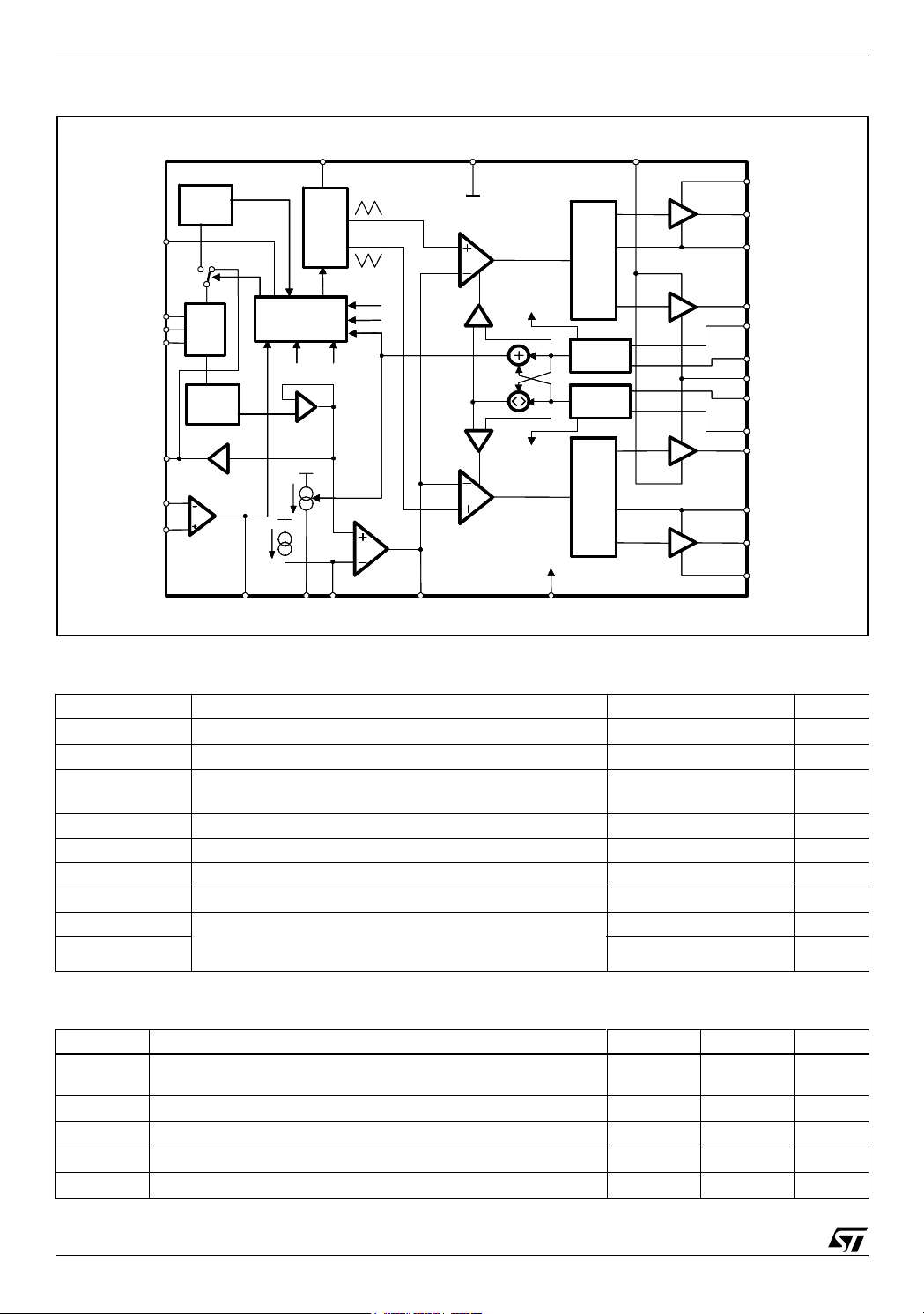
2 Description
The device implements a dual-phase step-down controller with a 180 phase-shift between each phase
gure 1. Packages
SO28
VFQFPN-36 (6x6x1.0mm)
Table 1. Order Codes
Package Tube Tape & Reel
SO
VFQFPN
L6712D,
L6712AD
L6712Q,
L6712AQ
L6712DTR,
L6712ADTR
L6712QTR,
L6712AQTR
optimized for high current DC/DC applications.
Output voltage can be programmed through the in-
tegrated DAC from 0.900V to 3.300V; programming the "111" code, an external reference from
0.800V to 3.300V is used for the regulation.
Programmable Remote Sense Amplifier avoids
use of external resistor divider and recovers losses along distribution line.
The device assures a fast protection against load
over current and Over / Under voltage.An internal
crowbar is provided turning on the low side mosfet
if Over-voltage is detected.
Output current is limited working in Constant Current mode: when Under Voltage is detected, the
device resets, restarting operation.
June 2005
Rev. 3
1/29
L6712A L6712
Figure 2. Block Diagram
BAND-GAP
BAND-GAP
REFERENCE
REFERENCE
PGOOD
PGOOD
VID2
VID2
VID1
VID1
VID0
VID0
REF_IN/OUT
REF_IN/OUT
FBG
FBG
FBR
FBR
DAC
DAC
DIGITAL
DIGITAL
SOFT-START
SOFT-START
REMOTE
REMOTE
AMPLIFIER
AMPLIFIER
OSC / INH SGND VCCDR
OSC / INH SGND VCCDR
PWM1
TOTAL
TOTAL
CURRENT
CURRENT
PWM1
CURRENT
CURRENT
PWM2
PWM2
CH1
CH1
OCP
OCP
CURRENT
CURRENT
CORRECTION
CORRECTION
AVG
AVG
CH2
CH2
OCP
OCP
CURRENT
CURRENT
CORRECTION
CORRECTION
Vcc
Vcc
VccCOMPFBVSEN
VccCOMPFBVSEN
LOGIC AND
LOGIC AND
PROTECTIONS
PROTECTIONS
CH1 OCP
CH1 OCP
V
V
PROG
PROG
DROOP
DROOP
I
I
FB_START
FB_START
I
I
DROOP
DROOP
2 PHASE
2 PHASE
OSCILLATOR
OSCILLATOR
CH2 OCP
CH2 OCP
VCC
VCC
VCCDR
VCCDR
ERROR
ERROR
AMPLIFIER
AMPLIFIER
LOGIC PW M
LOGIC PW M
ADAPTIVE ANTI
ADAPTIVE ANTI
CROSS CONDUCTION
CROSS CONDUCTION
CURRENT
CURRENT
READING
READING
CURRENT
CURRENT
READ ING
READ ING
LOGIC PW M
LOGIC PW M
ADAPTIVE ANTI
ADAPTIVE ANTI
CROSS CONDUCTION
CROSS CONDUCTION
HS
HS
LS
LS
HS
HS
BOOT1
BOOT1
UGATE1
UGATE1
PHASE1
PHASE1
LGATE1
LGATE1
ISEN1
ISEN1
PGNDS1
PGNDS1
PGND
PGND
PGNDS2
PGNDS2
ISEN2
ISEN2
LS
LS
LGATE2
LGATE2
PHASE2
PHASE2
UGATE2
UGATE2
BOOT2
BOOT2
Table 2. Absolute Maximum Ratings
Symbol Parameter Value Unit
V
, V
CC
CCDR
V
BOOT-VPHASE
V
UGATE1-VPHASE1
V
UGATE2-VPHASE2
To P G ND 15 V
Boot Voltage 15 V
15 V
LGATE1, PHASE1, LGATE2, PHASE2 to PGND -0.3 to Vcc+0.3 V
VID0 to VID2 -0.3 to 5 V
All other pins to PGND -0.3 to 7 V
V
PHASEx
UGATEX Pins Maximum Withstanding Voltage Range
OTHER PINS ±2000 V
Sustainable Peak Voltage. T<20ns @ 600kHz 26 V
±1500 V
Test Condition: CDF-AEC-Q100-002”Human Body Model”
Acceptance Criteria: “Normal Performance”
Table 3. Thermal Data
Symbol Parameter SO28 VFQFPN36 Unit
R
thj-amb
T
T
P
max
stg
T
MAX
Thermal Resistance Junction to Ambient
60 30 °C/W
4 layer PCB (2s2p)
Maximum junction temperature 150 150 °C
Storage temperature range -40 to 150 -40 to 150 °C
Junction Temperature Range -40 to 125 -40 to 125 °C
j
Max power dissipation at T
= 25°C 23.5W
amb
2/29
Figure 3. Pin Connection (Top view)
D
LGATE1
VCCDR
PHASE1
UGATE1
BOOT1
VCC
SGND
COMP
FB
DROOP
REF_IN/OUT
VSEN
ISEN1
PGNDS1
1
2
3
4
5
6
7
8
9
10
11
12
13
14
SO28
28
27
26
25
24
23
22
21
20
19
18
17
16
15
PGND
LGATE2
PHASE2
UGATE2
BOOT2
PGOOD
VID2
VID1
VID0
FBR
FBG
OSC/INH/FAULT
ISEN2
PGNDS2
L6712A L6712
BOOT2
PGOO
UGATE2
PHASE2
PHASE2
LGATE2
LGATE2
PGND
PGND
PGND
PGND
LGATE1
LGATE1
VCCDR
VCCDR
PHASE1
PHASE1
UGATE1
N.C.
27 26 25 24 23 22 21 20 19
27 26 25 24 23 22 21 20 19
28
28
29
29
30
30
31
31
32
32
33
33
34
34
35
35
36
36
1 2 3 4 5 6 7 8 9
1 2 3 4 5 6 7 8 9
N.C
N.C.
BOOT1
VID0
VID1
VID2
VCC
SGND
SGND
VFQFPN-36
Corner Pin internally connected to the Exposed Pad.
N.C.
FBG
FBR
OSC
OSC
18
18
17
17
N.C.
N.C.
ISEN2
ISEN2
16
16
PGNDS2
PGNDS2
15
15
PGNDS1
PGNDS1
14
14
ISEN1
ISEN1
13
13
VSEN
VSEN
12
12
REF_IN/OUT
REF_IN/OUT
11
11
10
10
N.C.
N.C.
FB
COMP
DROOP
Table 4. Electrical Characteristcs
(V
= 12V±10%, TJ = 0°C to 70°C unless otherwise specified)
CC
Symbol Parameter Test Condition Min. Typ. Max. Unit
Vcc SUPPLY CURRENT
I
CC
VCC supply current HGATEx and LGATEx open
VCCDR=BOOTx=12V
I
CCDR
I
BOOTx
VCCDR supply current LGATEx open; VCCDR=12V 1.5 3 4 mA
Boot supply current HGATEx open; PHASEx to
PGND; VCC=BOOTx=12V
POWER-ON
Turn-On VCC threshold VCC Rising; VCCDR=5V 8.2 9.2 10.2 V
Turn-Off VCC threshold VCC Falling; VCCDR=5V 6.5 7.5 8.5 V
Turn-On VCCDR
Threshold
Turn-Off VCCDR
Threshold
VCCDR Rising
VCC=12V
VCCDR Falling
VCC=12V
OSCILLATOR AND INHIBIT
f
OSC
Initial Accuracy OSC = OPEN
OSC = OPEN; Tj=0°C to 125°C
INH Inhibit threshold I
d
MAX
Maximum duty cycle
=5mA 0.5 V
SINK
L6712
, OSC = OPEN: I
OSC = OPEN; I
DROOP
DROOP
=70µA
L6712A, OSC = OPEN 85 90 %
∆Vosc Ramp Amplitude 3 V
FAULT Voltage at pin OSC OVP Active 4.75 5.0 5.25 V
7.5 10 12.5 mA
0.5 1 1.5 mA
4.2 4.4 4.6 V
4.0 4.2 4.4 V
135
150 165
127
=0
72
30
80
40
178
kHz
kHz
-
-
%
%
3/29

L6712A L6712
Table 4. Electrical Characteristcs (continued)
(V
= 12V±10%, TJ = 0°C to 70°C unless otherwise specified)
CC
Symbol Parameter Test Condition Min. Typ. Max. Unit
REFERENCE AND DAC
(1)
V
OUT
REF_IN/OUT Reference Accuracy VIDx See Table 5, VID ≠ “111” V
V
/ REF_IN/
PROG
OUT
REF_IN/OUT Input impedance 400 kΩ
I
VID
V
VID
VID
IL
VID
IH
ERROR AMPLIFIER
V
OS_EA
SR Slew-Rate COMP=10pF 15 V/µs
I
FB_START
DIFFERENTIAL AMPLIFIER (REMOTE BUFFER)
V
OS_RA
SR Slew Rate VSEN = 10pF 15 V/µs
DIFFERENTIAL CURRENT SENSING
, I
I
ISEN1
ISEN2
I
PGNDSx
I
, I
ISEN1
ISEN2
I
DROOP
GATE DRIVERS
t
RISE HGATE
I
HGATEx
R
HGATEx
t
RISE LGATE
I
LGATEx
R
LGATEx
Output Voltage Accuracy VIDx See Table 5, VID ≠ “11x“ -0.9 - 0.9 %
VID = “110“ -1.0 - 1.0 %
OUT
-5 V
OUTVOUT
+5 mV
Current Capability 3 mA
Load Regulation I
Accuracy with external
reference
= from 0 to 3mA 5.0 mV
REF
VID=“111”;
-2.0 2.0 %
REF_IN/OUT = 0.8V to 3.3V
VID pull-up Current VIDx =SGND 5 µA
VID pull-up Voltage VIDx = OPEN 3 V
VID Input Levels Input Low 0.4 V
Input High 1.0 V
Offset FB = COMP -5 5 mV
DC Gain 80 dB
Start-up Current FB=SGND; During Soft Start… 65 µA
Offset VSEN = FBG -8 8 mV
DC Gain 80 dB
Bias Current I
= 0 455055µA
LOAD
Bias Current 45 50 55 µA
Bias Current at
80 85 90 µA
Over Current Threshold
Droop Current I
High Side
Rise Time
High Side
≤ 001µA
LOAD
I
= 100% 47.5 50 52.5 µA
LOAD
BOOTx-PHASEx=10V;
C
to PHASEx=3.3nF
HGATEx
15 30 ns
BOOTx-PHASEx=10V 2 A
Source Current
High Side
BOOTx-PHASEx=12V; 1.5 2 2.5 Ω
Sink Resistance
Low Side
Rise Time
Low Side
VCCDR=10V;
C
to PGNDx=5.6nF
LGATEx
30 55 ns
VCCDR=10V 1.8 A
Source Current
Low Side
VCCDR=12V 0.7 1.1 1.5 Ω
Sink Resistance
4/29

L6712A L6712
Table 4. Electrical Characteristcs (continued)
(V
= 12V±10%, TJ = 0°C to 70°C unless otherwise specified)
CC
Symbol Parameter Test Condition Min. Typ. Max. Unit
PROTECTIONS
PGOOD Upper Threshold VSEN Rising 108 112 115 %
Lower Threshold VSEN Falling 84 88 92 %
OVP Over Voltage Threshold VSEN Rising 115 122 130 %
UVP Under Voltage Trip VSEN Falling 55 60 65 %
V
PGOODL
I
PGOODH
Note: 1. Output voltage is specified including Error Amplifier Offset in the trimming chain. Remote Amplifier is not included.
PGOOD Voltage Low I
PGOOD Leakage V
Table 5. Voltage Identification (VID) Codes.
VID2 VID1 VID0 Output Voltage (V)
111 Ext. Ref.
110 0.900
101 1.250
100 1.500
011 1.715
010 1.800
001 2.500
000 3.300
= -4mA 0.4 V
PGOOD
= 5V 1 µA
PGOOD
Table 6. Pin Function
N. (*)
SO VFQFPN
1 33 LGATE1 Channel 1 LS driver output.
2 34 VCCDR LS drivers supply: it can be varied from 5V to 12V buses.
3 35 PHASE1 Channel 1 HS driver return path. It must be connected to the HS1 mosfet source
4 36 UGATE1 Channel 1 HS driver output.
5 2 BOOT1 Channel 1 HS driver supply. This pin supplies the relative high side driver.
6 4 VCC Device supply voltage. The operative supply voltage is 12V ±10%.
7 5,6 SGND All the internal references are referred to this pin. Connect it to the PCB signal
8 7 COMP This pin is connected to the error amplifier output and is used to compensate the
9 8 FB This pin is connected to the error amplifier inverting input and is used to
Name
Description
A little series resistor helps in reducing device-dissipated power.
Filter locally with at least 1µF ceramic cap vs. PGND.
and provides the return path for the HS driver of channel 1.
A little series resistor helps in reducing device-dissipated power.
Connect through a capacitor (100nF typ.) to the PHASE1 pin and through a diode
to VCC (cathode vs. boot).
Filter with 1µF (Typ.) capacitor vs. GND.
ground.
control feedback loop.
compensate the control feedback loop.
5/29

L6712A L6712
Table 6. Pin Function (continued)
N. (*)
SO VFQFPN
10 9 DROOP A current proportional to the sum of the current sensed in both channel is
11 11 REF_IN /
12 12 VSEN Connected to the output voltage it is able to manage Over & Under-voltage
13 13 ISEN1 Channel 1 current sense pin. The output current may be sensed across a sense
14 14 PGNDS1 Channel 1 Power Ground sense pin. The net connecting the pin to the sense
15 15 PGNDS2 Channel 2 Power Ground sense pin. The net connecting the pin to the sense
16 16 ISEN2 Channel 2 current sense pin. The output current may be sensed across a sense
17 18 OSC/INH
18 20 FBG Remote sense amplifier inverting input. It has to be connected to the negative
19 21 FBR Remote sense amplifier non-inverting input. It has to be connected to the positive
Name
OUT
FAULT
Description
sourced from this pin (50µA at full load, 70µA at the Constant Current threshold).
Short to FB to implement the Droop effect: the resistor connected between FB
and VSEN (or the regulated output) allows programming the droop effect.
Otherwise, connect to GND directly or through a resistor (43kΩ max) and filter
with 1nF capacitor. In this last case, current information can be used for other
purposes.
Reference input/output. Filter vs. GND with 1nF ceramic capacitor (a total of
100nF capacitor is allowed).
It reproduces the reference used for the regulation following VID code: when
VID=111, the reference for the regulation must be connected on this pin.
References ranging from 0.800V up to 3.300V can be accepted.
conditions and the PGOOD signal. It is internally connected with the output of the
Remote Sense Amplifier for Remote Sense of the regulated voltage.
Connecting 1nF capacitor max vs. GND can help in reducing noise injection at
this pin.
If no Remote Sense is implemented, connect it directly to the regulated voltage in
order to manage OVP, UVP and PGOOD.
resistor or across the low-side mosfet R
low-side mosfet drain or to the sense resistor through a resistor Rg.
The net connecting the pin to the sense point must be routed as close as
possible to the PGNDS net in order to couple in common mode any picked-up
noise.
point must be routed as close as possible to the ISEN1 net in order to couple in
common mode any picked-up noise.
point must be routed as close as possible to the ISEN2 net in order to couple in
common mode any picked-up noise.
resistor or across the low-side mosfet R
low-side mosfet drain or to the sense resistor through a resistor Rg.
The net connecting the pin to the sense point must be routed as close as
possible to the PGNDS net in order to couple in common mode any picked-up
noise.
Oscillator pin.
It allows programming the switching frequency of each channel: the equivalent
switching frequency at the load side results in being doubled.
Internally fixed at 1.24V, the frequency is varied proportionally to the current sunk
(forced) from (into) the pin with an internal gain of 6kHz/µA (See relevant section
for details). If the pin is not connected, the switching frequency is 150kHz for
each channel (300kHz on the load).
The pin is forced high (5V Typ.) when an Over Voltage is detected; to recover
from this condition, cycle VCC.
Forcing the pin to a voltage lower than 0.6V, the device stops operation and
enters the inhibit state.
side of the load to perform programmable remote sensing through apposite
resistors (see relative section).
side of the load to perform programmable remote sensing through apposite
resistors (see relative section).
This pin has to be connected to the
dsON.
This pin has to be connected to the
dsON.
6/29
Table 6. Pin Function (continued)
L6712A L6712
N. (*)
SO VFQFPN
Name
Description
20 to 22 22 to 24 VID0-2 Voltage IDentification pins. These input are internally pulled-up. They are used to
program the output voltage as specified in Table 1 and to set the PGOOD, OVP
and UVP thresholds.
Connect to GND to program a ‘0’ while leave floating to program a ‘1’.
23 25 PGOOD This pin is an open collector output and is pulled low if the output voltage is not
within the above specified thresholds and during soft-start.
It cannot be pulled up above 5V. If not used may be left floating.
24 27 BOOT2 Channel 2 HS driver supply. This pin supplies the relative high side driver.
Connect through a capacitor (100nF typ.) to the PHASE2 pin and through a diode
to VCC (cathode vs. boot).
25 28 UGATE2 Channel 2 HS driver output.
A little series resistor helps in reducing device-dissipated power.
26 29 PHASE2 Channel 2 HS driver return path. It must be connected to the HS2 mosfet source
and provides the return path for the HS driver of channel 2.
27 30 LGATE2 Channel 2 LS driver output.
A little series resistor helps in reducing device-dissipated power.
28 31,
32
PGND LS drivers return path.
This pin is common to both sections and it must be connected through the
closest path to the LS mosfets source pins in order to reduce the noise injection
into the device.
PAD THERMAL
PA D
Thermal pad connects the silicon substrate and makes a good thermal contact
with the PCB to dissipate the power necessary to drive the external
mosfets.Connect to the GND plane with several vias to improve thermal
conductivity.
(*) Pin not reported in QFN column have to be considered as Not Connected, not internally bonded.
Figure 4. Reference Schematic
Vin
GNDin
VCCDR
BOOT1
HS1
L1
LS1
S2
S1
S0
UGATE1
PHASE1
LGATE1
ISEN1
Rg
PGNDS1
Rg
REF_IN/OUT
OSC / INH
L6712A
VID2
VID1
VID0
SGND
FBR FBG
L6712
VCC
BOOT2
UGATE2
PHASE2
LGATE2
ISEN2
PGNDS2
PGND
PGOOD
COMP
DROOP
FB
VSEN
C
IN
HS2
L2
C
LS2
Rg
Rg
C
R
R
OUT
LOAD
PGOOD
7/29

L6712A L6712
3 Device Description
The device is an integrated circuit realized in BCD technology. It provides complete control logic and protections for a high performance dual-phase step-down converter optimized for high current DC/DC applications. It is designed to drive N-Channel Mosfets in a two-phase synchronous-rectified buck topology. A
180 deg phase shift is provided between the two phases allowing reduction in the input capacitor current
ripple, reducing also the size and the losses. The output voltage of the converter can be precisely regulated, programming the VID pins, from 0.900 to 3.300V with a maximum tolerance of ±0.9% over temperature and line voltage variations. The programmable Remote Sense Amplifier avoids the use of external
resistor divider allowing recovering drops across distribution lines and also adjusting output voltage to different values from the available reference. The device provides an average current-mode control with fast
transient response. It includes a 150kHz free-running oscillator externally adjustable through a resistor.
The error amplifier features a 15V/µs slew rate that permits high converter bandwidth for fast transient performances. Current information is read across the lower mosfets R
in series to the LS mos in fully differential mode. The current information corrects the PWM outputs in order
to equalize the average current carried by each phase. Current sharing between the two phases is then
limited at ±10% over static and dynamic conditions unless considering the sensing element spread. Droop
effect can be programmed in order to minimize output filter and load transient response: the function can
be disabled and the current information available on the pin can be used for other purposes. The device
protects against Over-Current, with an OC threshold for each phase, entering in constant current mode.
Since the current is read across the low side mosfets, the device keeps constant the bottom of the inductors current triangular waveform. When an Under Voltage is detected the device resets with all mosfets
OFF and suddenly re-starts. The device also performs a crowbar Over-Voltage protection that immediately latches the operations turning ON the lower driver and driving high the FAULT pin.
or across a sense resistor placed
dsON
3.1 OSCILLATOR
The switching frequency is internally fixed at 150kHz. Each phase works at the frequency fixed by the oscillator so that the resulting switching frequency at the load side results in being doubled.
The internal oscillator generates the triangular waveform for the PWM charging and discharging with a
constant current an internal capacitor. The current delivered to the oscillator is typically 25µA
(Fsw=150kHz) and may be varied using an external resistor (R
) connected between OSC pin and
OSC
SGND or Vcc. Since the OSC pin is maintained at fixed voltage (Typ. 1.237V), the frequency is varied
proportionally to the current sunk (forced) from (into) the pin considering the internal gain of 6KHz/µA.
In particular connecting it to SGND the frequency is increased (current is sunk from the pin), while connecting R
to Vcc=12V the frequency is reduced (current is forced into the pin), according to the follow-
OSC
ing relationships:
6
⋅
KΩ[]
7
⋅
KΩ[]
kHz[]+=⋅+=
kHz[]–=⋅=
R
R
OSC
OSC
vs. GND:
vs. 12V:
1.237
F
F
SW
150 KH z[]
SW
150 KH z[]
---------------
R
OSC
12 1.237–
------------------------ -– 6
R
OSC
6
kHz
---------- -
µA
kHz
---------- -
µA
7.422 10
150 kHz[]
----------------------------- -
R
150 kH z[]
OSC
6.457 10
----------------------------- -
R
OSC
Forcing 25µA into this pin, the device stops switching because no current is delivered to the oscillator
8/29
L6712A L6712
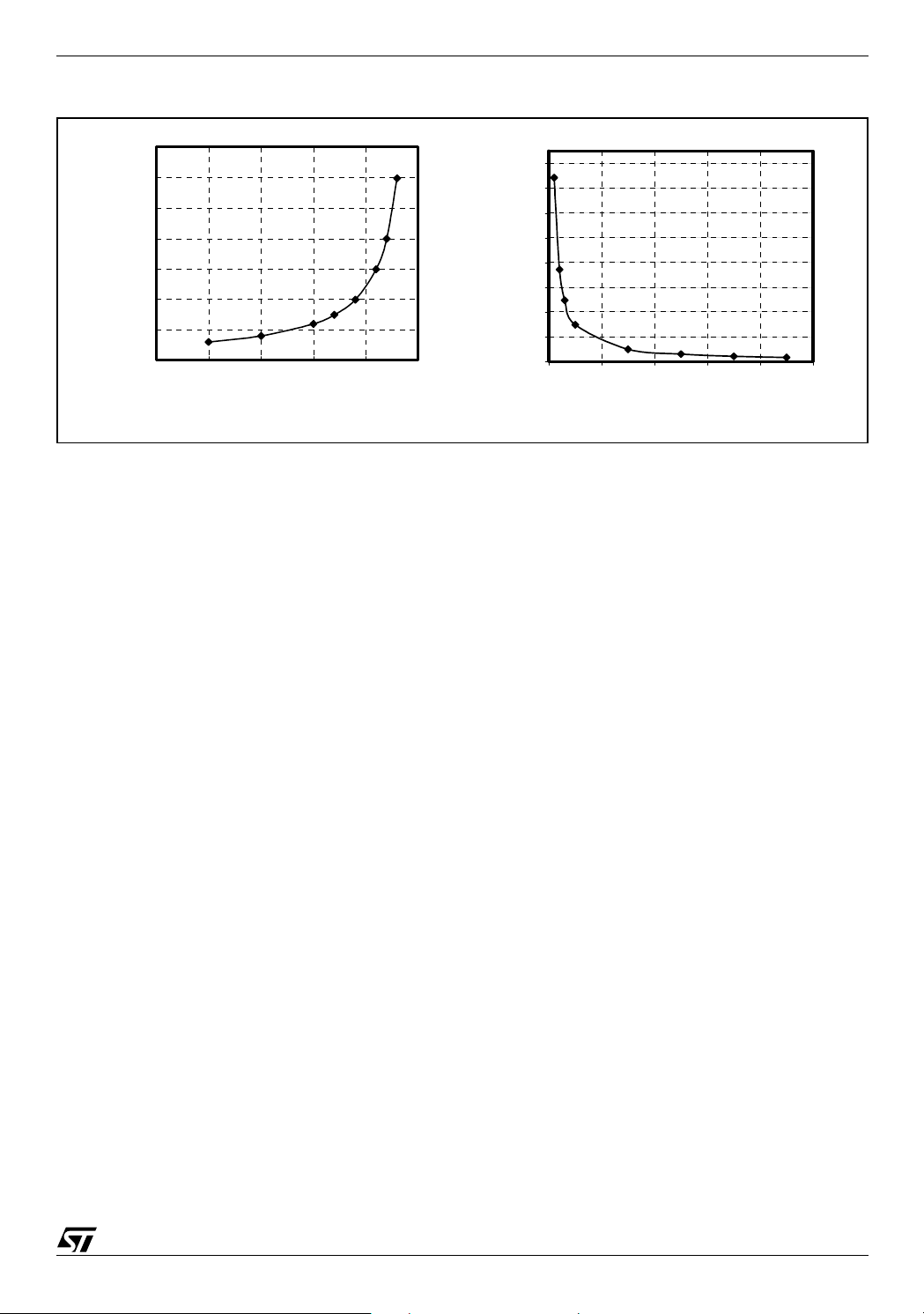
Figure 5. R
14000
12000
10000
8000
) vs. 12V
6000
4000
Rosc(K
2000
vs. Switching Frequency
OSC
0
25 50 75 100 125 150
Frequency (kHz)
800
700
600
500
) vs. GND
400
Ω
300
200
Rosc(K
100
0
150 250 350 450 550 650
Frequency (kHz)
3.2 DIGITAL TO ANALOG CONVERTER AND REFERENCE
The built-in digital to analog converter allows the adjustment of the output voltage from 0.900V to 3.300V
as shown in Figure 6. Different voltages can be reached simply changing the Remote Amplifier Gain that
acts as a resistor divider (See relevant section).
The internal reference is trimmed during production process to have an output voltage accuracy of ±0.9%
and a zero temperature coefficient around 70°C including also error amplifier offset compensation. It is
programmed through the voltage identification (VID) pins. These are inputs of an internal DAC that is realized by means of a series of resistors providing a partition of the internal voltage reference. The VID code
drives a multiplexer that select a voltage on a precise point of the divider (see Figure 6). The DAC output
is delivered to an amplifier obtaining the V
voltage reference (i.e. the set-point of the error amplifier).
PROG
Internal pull-ups are provided (realized with a 5µA current generator up to 3V typ.); in this way, to program
a logic "1" it is enough to leave the pin floating, while to program a logic "0" it is enough to short the pin to
SGND.
The device offers a bi-directional pin REF_IN/OUT: the internal reference used for the regulation is usually
available on this pin with 3mA of maximum current capability except when VID code 111 is programmed;
in this case the device accepts an external reference through the REF_IN/OUT pin and regulates on it.
When external reference is used, it must range from 0.800V up to 3.300V to assure proper functionality of
the device.
Figure 6 shows a block schematic of how the Reference for the regulation is managed when internal or
external reference is used.
The voltage identification (VID) pin configuration or the external reference provided also sets the powergood thresholds (PGOOD) and the Over/Under voltage protection (OVP/UVP) thresholds.
9/29
 Loading...