

Page 1
L6712
Fi
L6712A
TWO-PHASE INTERLEAVED DC/DC CONTROLLER
1 Features
■ 2 PHASE OPERATION WITH
SYNCHRONOUS RECTIFIER CONTROL
■ ULTRA FAST LOAD TRANSIENT RESPONSE
■ INTEGRATED HIGH CURRENT GATE
DRIVERS: UP TO 2A GATE CURRENT
■
3 BIT PROGRAMMABLE OUTPUT FROM
0.900V TO 3.300V OR WITH EXTERNAL REF.
■ ±0.9% OUTPUT VOLTAGE ACCURACY
■ 3mA CAPABLE AVAILABLE REFERENCE
■ INTEGRATED PROGRAMMABLE REMOTE
SENSE AMPLIFIER
■ PROGRAMMABLE DROOP EFFECT
■ 10% ACTIVE CURRENT SHARING
ACCURACY
■ DIGITAL 2048 STEP SOFT-START
■
CROWBAR LATCHED OVERVOLTAGE PROT.
■ NON-LATCHED UNDERVOLTAGE PROT.
■ OVERCURRENT PROTECTION REALIZED
USING THE LOWER MOSFET'S R
dsON
OR A
SENSE RESISTOR
■ OSCILLATOR EXTERNALLY ADJUSTABLE
AND INTERNALLY FIXED AT 150kHZ
■ POWER GOOD OUTPUT AND INHIBIT
FUNCTION
■ PACKAGES: SO-28 & VFQFPN-36
1.1 Applications
■ HIGH CURRENT DC/DC CONVERTERS
■ DISTRIBUTED POWER SUPPLY
2 Description
The device implements a dual-phase step-down controller with a 180 phase-shift between each phase
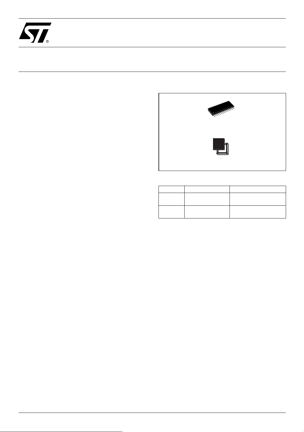
gure 1. Packages
SO28
VFQFPN-36 (6x6x1.0mm)
Table 1. Order Codes
Package Tube Tape & Reel
SO
VFQFPN
L6712D,
L6712AD
L6712Q,
L6712AQ
L6712DTR,
L6712ADTR
L6712QTR,
L6712AQTR
optimized for high current DC/DC applications.
Output voltage can be programmed through the in-
tegrated DAC from 0.900V to 3.300V; programming the "111" code, an external reference from
0.800V to 3.300V is used for the regulation.
Programmable Remote Sense Amplifier avoids
use of external resistor divider and recovers losses along distribution line.
The device assures a fast protection against load
over current and Over / Under voltage.An internal
crowbar is provided turning on the low side mosfet
if Over-voltage is detected.
Output current is limited working in Constant Current mode: when Under Voltage is detected, the
device resets, restarting operation.
June 2005
Rev. 3
1/29
Page 2
L6712A L6712
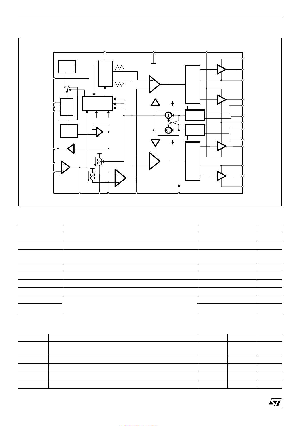
Figure 2. Block Diagram
BAND-GAP
BAND-GAP
REFERENCE
REFERENCE
PGOOD
PGOOD
VID2
VID2
VID1
VID1
VID0
VID0
REF_IN/OUT
REF_IN/OUT
FBG
FBG
FBR
FBR
DAC
DAC
DIGITAL
DIGITAL
SOFT-START
SOFT-START
REMOTE
REMOTE
AMPLIFIER
AMPLIFIER
OSC / INH SGND VCCDR
OSC / INH SGND VCCDR
PWM1
TOTAL
TOTAL
CURRENT
CURRENT
PWM1
CURRENT
CURRENT
PWM2
PWM2
CH1
CH1
OCP
OCP
CURRENT
CURRENT
CORRECTION
CORRECTION
AVG
AVG
CH2
CH2
OCP
OCP
CURRENT
CURRENT
CORRECTION
CORRECTION
Vcc
Vcc
VccCOMPFBVSEN
VccCOMPFBVSEN
LOGIC AND
LOGIC AND
PROTECTIONS
PROTECTIONS
CH1 OCP
CH1 OCP
V
V
PROG
PROG
DROOP
DROOP
I
I
FB_START
FB_START
I
I
DROOP
DROOP
2 PHASE
2 PHASE
OSCILLATOR
OSCILLATOR
CH2 OCP
CH2 OCP
VCC
VCC
VCCDR
VCCDR
ERROR
ERROR
AMPLIFIER
AMPLIFIER
LOGIC PW M
LOGIC PW M
ADAPTIVE ANTI
ADAPTIVE ANTI
CROSS CONDUCTION
CROSS CONDUCTION
CURRENT
CURRENT
READING
READING
CURRENT
CURRENT
READ ING
READ ING
LOGIC PW M
LOGIC PW M
ADAPTIVE ANTI
ADAPTIVE ANTI
CROSS CONDUCTION
CROSS CONDUCTION
HS
HS
LS
LS
HS
HS
BOOT1
BOOT1
UGATE1
UGATE1
PHASE1
PHASE1
LGATE1
LGATE1
ISEN1
ISEN1
PGNDS1
PGNDS1
PGND
PGND
PGNDS2
PGNDS2
ISEN2
ISEN2
LS
LS
LGATE2
LGATE2
PHASE2
PHASE2
UGATE2
UGATE2
BOOT2
BOOT2
Table 2. Absolute Maximum Ratings
Symbol Parameter Value Unit
V
, V
CC
CCDR
V
BOOT-VPHASE
V
UGATE1-VPHASE1
V
UGATE2-VPHASE2
To P G ND 15 V
Boot Voltage 15 V
15 V
LGATE1, PHASE1, LGATE2, PHASE2 to PGND -0.3 to Vcc+0.3 V
VID0 to VID2 -0.3 to 5 V
All other pins to PGND -0.3 to 7 V
V
PHASEx
UGATEX Pins Maximum Withstanding Voltage Range
OTHER PINS ±2000 V
Sustainable Peak Voltage. T<20ns @ 600kHz 26 V
±1500 V
Test Condition: CDF-AEC-Q100-002”Human Body Model”
Acceptance Criteria: “Normal Performance”
Table 3. Thermal Data
Symbol Parameter SO28 VFQFPN36 Unit
R
thj-amb
T
T
P
max
stg
T
MAX
Thermal Resistance Junction to Ambient
60 30 °C/W
4 layer PCB (2s2p)
Maximum junction temperature 150 150 °C
Storage temperature range -40 to 150 -40 to 150 °C
Junction Temperature Range -40 to 125 -40 to 125 °C
j
Max power dissipation at T
= 25°C 23.5W
amb
2/29
Page 3
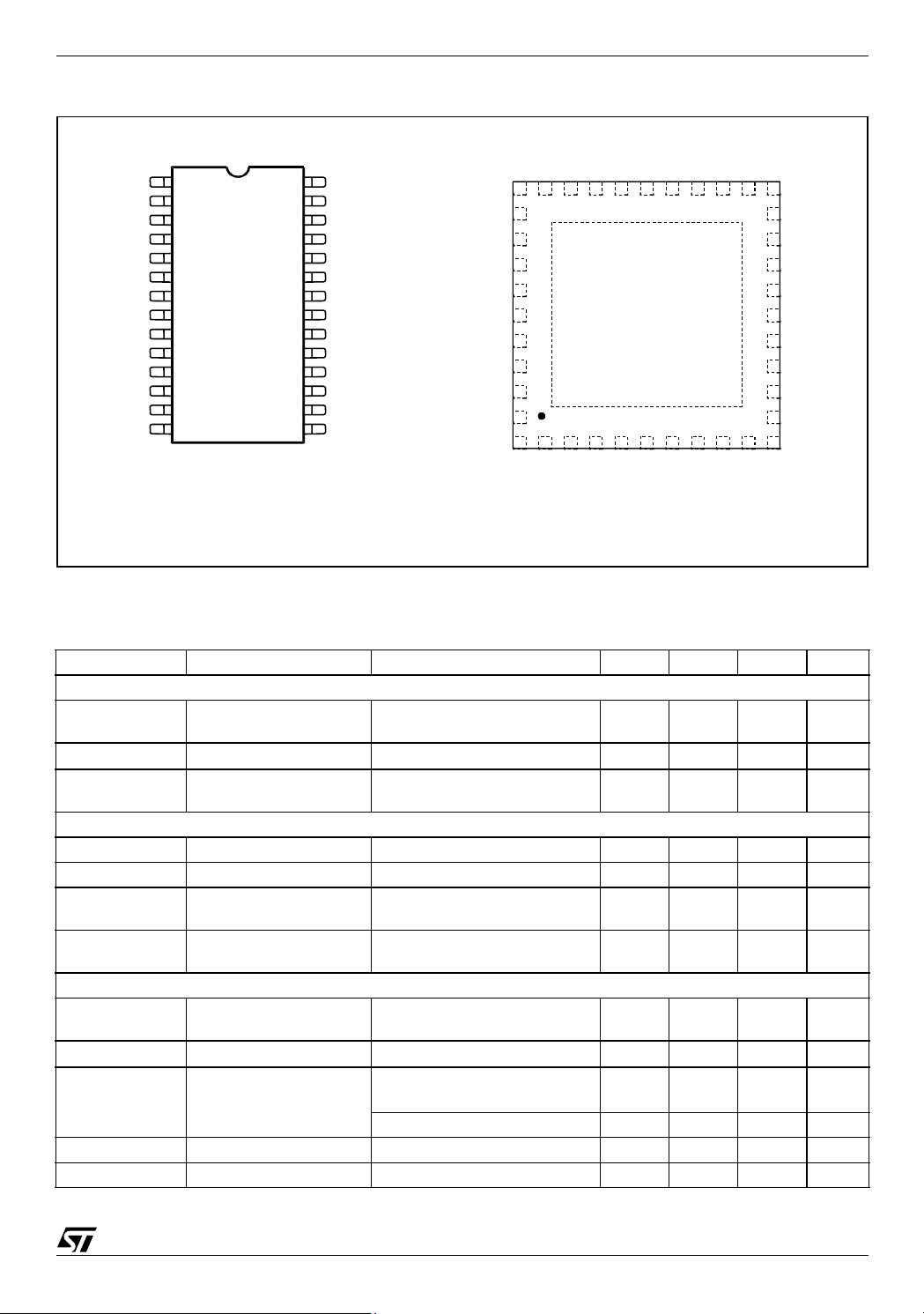
Figure 3. Pin Connection (Top view)
D
LGATE1
VCCDR
PHASE1
UGATE1
BOOT1
VCC
SGND
COMP
FB
DROOP
REF_IN/OUT
VSEN
ISEN1
PGNDS1
1
2
3
4
5
6
7
8
9
10
11
12
13
14
SO28
28
27
26
25
24
23
22
21
20
19
18
17
16
15
PGND
LGATE2
PHASE2
UGATE2
BOOT2
PGOOD
VID2
VID1
VID0
FBR
FBG
OSC/INH/FAULT
ISEN2
PGNDS2
L6712A L6712
BOOT2
PGOO
UGATE2
PHASE2
PHASE2
LGATE2
LGATE2
PGND
PGND
PGND
PGND
LGATE1
LGATE1
VCCDR
VCCDR
PHASE1
PHASE1
UGATE1
N.C.
27 26 25 24 23 22 21 20 19
27 26 25 24 23 22 21 20 19
28
28
29
29
30
30
31
31
32
32
33
33
34
34
35
35
36
36
1 2 3 4 5 6 7 8 9
1 2 3 4 5 6 7 8 9
N.C
N.C.
BOOT1
VID0
VID1
VID2
VCC
SGND
SGND
VFQFPN-36
Corner Pin internally connected to the Exposed Pad.
N.C.
FBG
FBR
OSC
OSC
18
18
17
17
N.C.
N.C.
ISEN2
ISEN2
16
16
PGNDS2
PGNDS2
15
15
PGNDS1
PGNDS1
14
14
ISEN1
ISEN1
13
13
VSEN
VSEN
12
12
REF_IN/OUT
REF_IN/OUT
11
11
10
10
N.C.
N.C.
FB
COMP
DROOP
Table 4. Electrical Characteristcs
(V
= 12V±10%, TJ = 0°C to 70°C unless otherwise specified)
CC
Symbol Parameter Test Condition Min. Typ. Max. Unit
Vcc SUPPLY CURRENT
I
CC
VCC supply current HGATEx and LGATEx open
VCCDR=BOOTx=12V
I
CCDR
I
BOOTx
VCCDR supply current LGATEx open; VCCDR=12V 1.5 3 4 mA
Boot supply current HGATEx open; PHASEx to
PGND; VCC=BOOTx=12V
POWER-ON
Turn-On VCC threshold VCC Rising; VCCDR=5V 8.2 9.2 10.2 V
Turn-Off VCC threshold VCC Falling; VCCDR=5V 6.5 7.5 8.5 V
Turn-On VCCDR
Threshold
Turn-Off VCCDR
Threshold
VCCDR Rising
VCC=12V
VCCDR Falling
VCC=12V
OSCILLATOR AND INHIBIT
f
OSC
Initial Accuracy OSC = OPEN
OSC = OPEN; Tj=0°C to 125°C
INH Inhibit threshold I
d
MAX
Maximum duty cycle
=5mA 0.5 V
SINK
L6712
, OSC = OPEN: I
OSC = OPEN; I
DROOP
DROOP
=70µA
L6712A, OSC = OPEN 85 90 %
∆Vosc Ramp Amplitude 3 V
FAULT Voltage at pin OSC OVP Active 4.75 5.0 5.25 V
7.5 10 12.5 mA
0.5 1 1.5 mA
4.2 4.4 4.6 V
4.0 4.2 4.4 V
135
150 165
127
=0
72
30
80
40
178
kHz
kHz
-
-
%
%
3/29
Page 4

L6712A L6712
Table 4. Electrical Characteristcs (continued)
(V
= 12V±10%, TJ = 0°C to 70°C unless otherwise specified)
CC
Symbol Parameter Test Condition Min. Typ. Max. Unit
REFERENCE AND DAC
(1)
V
OUT
REF_IN/OUT Reference Accuracy VIDx See Table 5, VID ≠ “111” V
V
/ REF_IN/
PROG
OUT
REF_IN/OUT Input impedance 400 kΩ
I
VID
V
VID
VID
IL
VID
IH
ERROR AMPLIFIER
V
OS_EA
SR Slew-Rate COMP=10pF 15 V/µs
I
FB_START
DIFFERENTIAL AMPLIFIER (REMOTE BUFFER)
V
OS_RA
SR Slew Rate VSEN = 10pF 15 V/µs
DIFFERENTIAL CURRENT SENSING
, I
I
ISEN1
ISEN2
I
PGNDSx
I
, I
ISEN1
ISEN2
I
DROOP
GATE DRIVERS
t
RISE HGATE
I
HGATEx
R
HGATEx
t
RISE LGATE
I
LGATEx
R
LGATEx
Output Voltage Accuracy VIDx See Table 5, VID ≠ “11x“ -0.9 - 0.9 %
VID = “110“ -1.0 - 1.0 %
OUT
-5 V
OUTVOUT
+5 mV
Current Capability 3 mA
Load Regulation I
Accuracy with external
reference
= from 0 to 3mA 5.0 mV
REF
VID=“111”;
-2.0 2.0 %
REF_IN/OUT = 0.8V to 3.3V
VID pull-up Current VIDx =SGND 5 µA
VID pull-up Voltage VIDx = OPEN 3 V
VID Input Levels Input Low 0.4 V
Input High 1.0 V
Offset FB = COMP -5 5 mV
DC Gain 80 dB
Start-up Current FB=SGND; During Soft Start… 65 µA
Offset VSEN = FBG -8 8 mV
DC Gain 80 dB
Bias Current I
= 0 455055µA
LOAD
Bias Current 45 50 55 µA
Bias Current at
80 85 90 µA
Over Current Threshold
Droop Current I
High Side
Rise Time
High Side
≤ 001µA
LOAD
I
= 100% 47.5 50 52.5 µA
LOAD
BOOTx-PHASEx=10V;
C
to PHASEx=3.3nF
HGATEx
15 30 ns
BOOTx-PHASEx=10V 2 A
Source Current
High Side
BOOTx-PHASEx=12V; 1.5 2 2.5 Ω
Sink Resistance
Low Side
Rise Time
Low Side
VCCDR=10V;
C
to PGNDx=5.6nF
LGATEx
30 55 ns
VCCDR=10V 1.8 A
Source Current
Low Side
VCCDR=12V 0.7 1.1 1.5 Ω
Sink Resistance
4/29
Page 5

L6712A L6712
Table 4. Electrical Characteristcs (continued)
(V
= 12V±10%, TJ = 0°C to 70°C unless otherwise specified)
CC
Symbol Parameter Test Condition Min. Typ. Max. Unit
PROTECTIONS
PGOOD Upper Threshold VSEN Rising 108 112 115 %
Lower Threshold VSEN Falling 84 88 92 %
OVP Over Voltage Threshold VSEN Rising 115 122 130 %
UVP Under Voltage Trip VSEN Falling 55 60 65 %
V
PGOODL
I
PGOODH
Note: 1. Output voltage is specified including Error Amplifier Offset in the trimming chain. Remote Amplifier is not included.
PGOOD Voltage Low I
PGOOD Leakage V
Table 5. Voltage Identification (VID) Codes.
VID2 VID1 VID0 Output Voltage (V)
111 Ext. Ref.
110 0.900
101 1.250
100 1.500
011 1.715
010 1.800
001 2.500
000 3.300
= -4mA 0.4 V
PGOOD
= 5V 1 µA
PGOOD
Table 6. Pin Function
N. (*)
SO VFQFPN
1 33 LGATE1 Channel 1 LS driver output.
2 34 VCCDR LS drivers supply: it can be varied from 5V to 12V buses.
3 35 PHASE1 Channel 1 HS driver return path. It must be connected to the HS1 mosfet source
4 36 UGATE1 Channel 1 HS driver output.
5 2 BOOT1 Channel 1 HS driver supply. This pin supplies the relative high side driver.
6 4 VCC Device supply voltage. The operative supply voltage is 12V ±10%.
7 5,6 SGND All the internal references are referred to this pin. Connect it to the PCB signal
8 7 COMP This pin is connected to the error amplifier output and is used to compensate the
9 8 FB This pin is connected to the error amplifier inverting input and is used to
Name
Description
A little series resistor helps in reducing device-dissipated power.
Filter locally with at least 1µF ceramic cap vs. PGND.
and provides the return path for the HS driver of channel 1.
A little series resistor helps in reducing device-dissipated power.
Connect through a capacitor (100nF typ.) to the PHASE1 pin and through a diode
to VCC (cathode vs. boot).
Filter with 1µF (Typ.) capacitor vs. GND.
ground.
control feedback loop.
compensate the control feedback loop.
5/29
Page 6

L6712A L6712
Table 6. Pin Function (continued)
N. (*)
SO VFQFPN
10 9 DROOP A current proportional to the sum of the current sensed in both channel is
11 11 REF_IN /
12 12 VSEN Connected to the output voltage it is able to manage Over & Under-voltage
13 13 ISEN1 Channel 1 current sense pin. The output current may be sensed across a sense
14 14 PGNDS1 Channel 1 Power Ground sense pin. The net connecting the pin to the sense
15 15 PGNDS2 Channel 2 Power Ground sense pin. The net connecting the pin to the sense
16 16 ISEN2 Channel 2 current sense pin. The output current may be sensed across a sense
17 18 OSC/INH
18 20 FBG Remote sense amplifier inverting input. It has to be connected to the negative
19 21 FBR Remote sense amplifier non-inverting input. It has to be connected to the positive
Name
OUT
FAULT
Description
sourced from this pin (50µA at full load, 70µA at the Constant Current threshold).
Short to FB to implement the Droop effect: the resistor connected between FB
and VSEN (or the regulated output) allows programming the droop effect.
Otherwise, connect to GND directly or through a resistor (43kΩ max) and filter
with 1nF capacitor. In this last case, current information can be used for other
purposes.
Reference input/output. Filter vs. GND with 1nF ceramic capacitor (a total of
100nF capacitor is allowed).
It reproduces the reference used for the regulation following VID code: when
VID=111, the reference for the regulation must be connected on this pin.
References ranging from 0.800V up to 3.300V can be accepted.
conditions and the PGOOD signal. It is internally connected with the output of the
Remote Sense Amplifier for Remote Sense of the regulated voltage.
Connecting 1nF capacitor max vs. GND can help in reducing noise injection at
this pin.
If no Remote Sense is implemented, connect it directly to the regulated voltage in
order to manage OVP, UVP and PGOOD.
resistor or across the low-side mosfet R
low-side mosfet drain or to the sense resistor through a resistor Rg.
The net connecting the pin to the sense point must be routed as close as
possible to the PGNDS net in order to couple in common mode any picked-up
noise.
point must be routed as close as possible to the ISEN1 net in order to couple in
common mode any picked-up noise.
point must be routed as close as possible to the ISEN2 net in order to couple in
common mode any picked-up noise.
resistor or across the low-side mosfet R
low-side mosfet drain or to the sense resistor through a resistor Rg.
The net connecting the pin to the sense point must be routed as close as
possible to the PGNDS net in order to couple in common mode any picked-up
noise.
Oscillator pin.
It allows programming the switching frequency of each channel: the equivalent
switching frequency at the load side results in being doubled.
Internally fixed at 1.24V, the frequency is varied proportionally to the current sunk
(forced) from (into) the pin with an internal gain of 6kHz/µA (See relevant section
for details). If the pin is not connected, the switching frequency is 150kHz for
each channel (300kHz on the load).
The pin is forced high (5V Typ.) when an Over Voltage is detected; to recover
from this condition, cycle VCC.
Forcing the pin to a voltage lower than 0.6V, the device stops operation and
enters the inhibit state.
side of the load to perform programmable remote sensing through apposite
resistors (see relative section).
side of the load to perform programmable remote sensing through apposite
resistors (see relative section).
This pin has to be connected to the
dsON.
This pin has to be connected to the
dsON.
6/29
Page 7
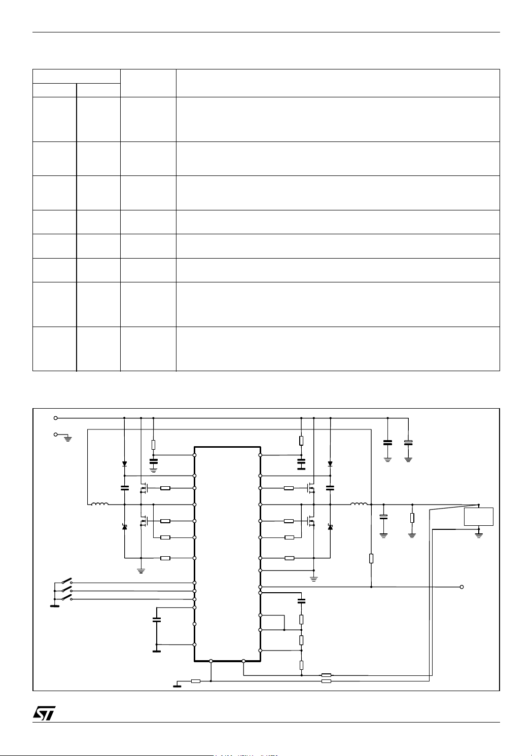
Table 6. Pin Function (continued)
L6712A L6712
N. (*)
SO VFQFPN
Name
Description
20 to 22 22 to 24 VID0-2 Voltage IDentification pins. These input are internally pulled-up. They are used to
program the output voltage as specified in Table 1 and to set the PGOOD, OVP
and UVP thresholds.
Connect to GND to program a ‘0’ while leave floating to program a ‘1’.
23 25 PGOOD This pin is an open collector output and is pulled low if the output voltage is not
within the above specified thresholds and during soft-start.
It cannot be pulled up above 5V. If not used may be left floating.
24 27 BOOT2 Channel 2 HS driver supply. This pin supplies the relative high side driver.
Connect through a capacitor (100nF typ.) to the PHASE2 pin and through a diode
to VCC (cathode vs. boot).
25 28 UGATE2 Channel 2 HS driver output.
A little series resistor helps in reducing device-dissipated power.
26 29 PHASE2 Channel 2 HS driver return path. It must be connected to the HS2 mosfet source
and provides the return path for the HS driver of channel 2.
27 30 LGATE2 Channel 2 LS driver output.
A little series resistor helps in reducing device-dissipated power.
28 31,
32
PGND LS drivers return path.
This pin is common to both sections and it must be connected through the
closest path to the LS mosfets source pins in order to reduce the noise injection
into the device.
PAD THERMAL
PA D
Thermal pad connects the silicon substrate and makes a good thermal contact
with the PCB to dissipate the power necessary to drive the external
mosfets.Connect to the GND plane with several vias to improve thermal
conductivity.
(*) Pin not reported in QFN column have to be considered as Not Connected, not internally bonded.
Figure 4. Reference Schematic
Vin
GNDin
VCCDR
BOOT1
HS1
L1
LS1
S2
S1
S0
UGATE1
PHASE1
LGATE1
ISEN1
Rg
PGNDS1
Rg
REF_IN/OUT
OSC / INH
L6712A
VID2
VID1
VID0
SGND
FBR FBG
L6712
VCC
BOOT2
UGATE2
PHASE2
LGATE2
ISEN2
PGNDS2
PGND
PGOOD
COMP
DROOP
FB
VSEN
C
IN
HS2
L2
C
LS2
Rg
Rg
C
R
R
OUT
LOAD
PGOOD
7/29
Page 8

L6712A L6712
3 Device Description
The device is an integrated circuit realized in BCD technology. It provides complete control logic and protections for a high performance dual-phase step-down converter optimized for high current DC/DC applications. It is designed to drive N-Channel Mosfets in a two-phase synchronous-rectified buck topology. A
180 deg phase shift is provided between the two phases allowing reduction in the input capacitor current
ripple, reducing also the size and the losses. The output voltage of the converter can be precisely regulated, programming the VID pins, from 0.900 to 3.300V with a maximum tolerance of ±0.9% over temperature and line voltage variations. The programmable Remote Sense Amplifier avoids the use of external
resistor divider allowing recovering drops across distribution lines and also adjusting output voltage to different values from the available reference. The device provides an average current-mode control with fast
transient response. It includes a 150kHz free-running oscillator externally adjustable through a resistor.
The error amplifier features a 15V/µs slew rate that permits high converter bandwidth for fast transient performances. Current information is read across the lower mosfets R
in series to the LS mos in fully differential mode. The current information corrects the PWM outputs in order
to equalize the average current carried by each phase. Current sharing between the two phases is then
limited at ±10% over static and dynamic conditions unless considering the sensing element spread. Droop
effect can be programmed in order to minimize output filter and load transient response: the function can
be disabled and the current information available on the pin can be used for other purposes. The device
protects against Over-Current, with an OC threshold for each phase, entering in constant current mode.
Since the current is read across the low side mosfets, the device keeps constant the bottom of the inductors current triangular waveform. When an Under Voltage is detected the device resets with all mosfets
OFF and suddenly re-starts. The device also performs a crowbar Over-Voltage protection that immediately latches the operations turning ON the lower driver and driving high the FAULT pin.
or across a sense resistor placed
dsON
3.1 OSCILLATOR
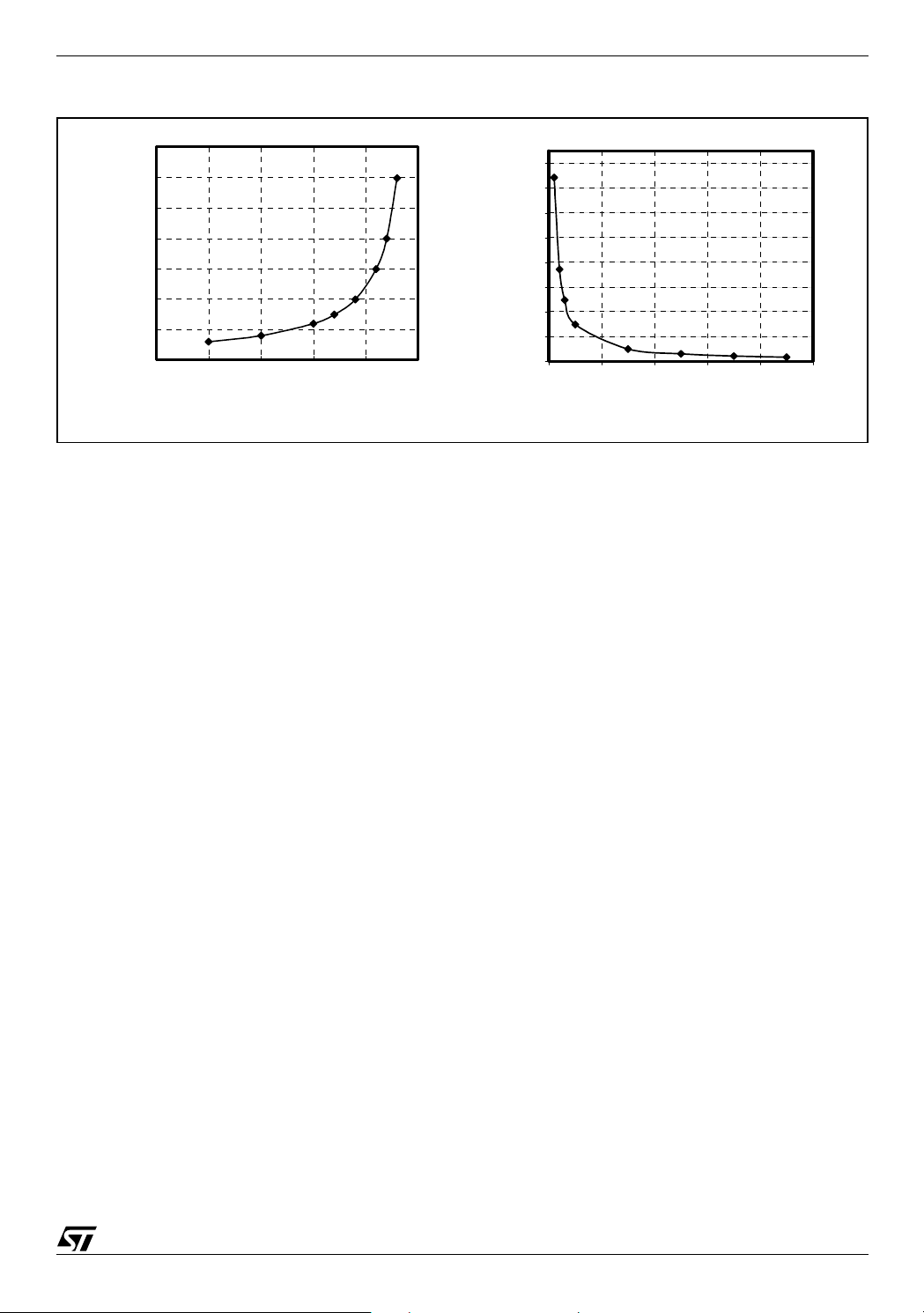
The switching frequency is internally fixed at 150kHz. Each phase works at the frequency fixed by the oscillator so that the resulting switching frequency at the load side results in being doubled.
The internal oscillator generates the triangular waveform for the PWM charging and discharging with a
constant current an internal capacitor. The current delivered to the oscillator is typically 25µA
(Fsw=150kHz) and may be varied using an external resistor (R
) connected between OSC pin and
OSC
SGND or Vcc. Since the OSC pin is maintained at fixed voltage (Typ. 1.237V), the frequency is varied
proportionally to the current sunk (forced) from (into) the pin considering the internal gain of 6KHz/µA.
In particular connecting it to SGND the frequency is increased (current is sunk from the pin), while connecting R
to Vcc=12V the frequency is reduced (current is forced into the pin), according to the follow-
OSC
ing relationships:
6
⋅
KΩ[]
7
⋅
KΩ[]
kHz[]+=⋅+=
kHz[]–=⋅=
R
R
OSC
OSC
vs. GND:
vs. 12V:
1.237
F
F
SW
150 KH z[]
SW
150 KH z[]
---------------
R
OSC
12 1.237–
------------------------ -– 6
R
OSC
6
kHz
---------- -
µA
kHz
---------- -
µA
7.422 10
150 kHz[]
----------------------------- -
R
150 kH z[]
OSC
6.457 10
----------------------------- -
R
OSC
Forcing 25µA into this pin, the device stops switching because no current is delivered to the oscillator
8/29
Page 9
L6712A L6712
Figure 5. R
14000
12000
10000
8000
) vs. 12V
6000
4000
Rosc(K
2000
vs. Switching Frequency
OSC
0
25 50 75 100 125 150
Frequency (kHz)
800
700
600
500
) vs. GND
400
Ω
300
200
Rosc(K
100
0
150 250 350 450 550 650
Frequency (kHz)
3.2 DIGITAL TO ANALOG CONVERTER AND REFERENCE
The built-in digital to analog converter allows the adjustment of the output voltage from 0.900V to 3.300V
as shown in Figure 6. Different voltages can be reached simply changing the Remote Amplifier Gain that
acts as a resistor divider (See relevant section).
The internal reference is trimmed during production process to have an output voltage accuracy of ±0.9%
and a zero temperature coefficient around 70°C including also error amplifier offset compensation. It is
programmed through the voltage identification (VID) pins. These are inputs of an internal DAC that is realized by means of a series of resistors providing a partition of the internal voltage reference. The VID code
drives a multiplexer that select a voltage on a precise point of the divider (see Figure 6). The DAC output
is delivered to an amplifier obtaining the V
voltage reference (i.e. the set-point of the error amplifier).
PROG
Internal pull-ups are provided (realized with a 5µA current generator up to 3V typ.); in this way, to program
a logic "1" it is enough to leave the pin floating, while to program a logic "0" it is enough to short the pin to
SGND.
The device offers a bi-directional pin REF_IN/OUT: the internal reference used for the regulation is usually
available on this pin with 3mA of maximum current capability except when VID code 111 is programmed;
in this case the device accepts an external reference through the REF_IN/OUT pin and regulates on it.
When external reference is used, it must range from 0.800V up to 3.300V to assure proper functionality of
the device.
Figure 6 shows a block schematic of how the Reference for the regulation is managed when internal or
external reference is used.
The voltage identification (VID) pin configuration or the external reference provided also sets the powergood thresholds (PGOOD) and the Over/Under voltage protection (OVP/UVP) thresholds.
9/29
Page 10

L6712A L6712
Figure 6. Reference Management
BAND-GAP
REFERENCE
(1.235V)
CONTROL
LOGIC
VIDx
INTERNAL REFERENCE
EXTERNAL REFERENCE
ERROR
VID3
VID2
VID1
REF_IN/OUT
DAC
AMPLIFIER
DIGITAL
SOFT-START
V
PROG
FB
COMP
The output regulated voltage accuracy can be extracted from the following relationships (worst case condition):
V
OU T _TOT_ACC
%[] V
OUT_ACC
%[]K
OS
V
OS_RA
--------------------
V
OUT
100⋅⋅+ 0.9%±()K
OS
8mV±()
---------------------
V
OUT
100⋅⋅+==
(worst case with internal reference)
V
OU T _TOT_ACC
%[]EXT_REF_Accuracy[%]
V
PROG
-------------------------------------
REF_IN/OUT
[%]
⎝⎠
EXT_REF
100⋅
V
OS_EA
⎛⎞
-------------------------- -
V
OS_RA
--------------------
K
OS
V
100=⋅⋅++ +=
OUT
⎛⎞
EX T _REF _Accuracy [%] 2.0%±()
-------------------------- -
⎝⎠
EXT_REF
5mV±()
100⋅
K
OS
8mV±()
---------------------
V
out
100⋅⋅++ +=
(worst case with external reference)
where V
tively and K
and V
OS_RA
= 1+1/RA_Gain reflects the impact of the Remote Amplifier Gain (RA_Gain) on the regula-
OS
are the offsets related to the Error Amplifier and the Remote Amplifier respec-
OS_EA
tion (see relevant section).
A statistical analysis could consider applying the root-sum-square (RSS) method to calculate the precision
since all the variables are statistically independent as follow:
2
100⋅⋅
V
OU T _TOT_ACC
[%] V
=
OUT_ACC
2
+
[%]()
V
OS
OS_RA
--------------------
V
OUT
⎛⎞
K
⎝⎠
(with internal reference)
V
OU T _TOT_ACC
V
[%] = EXT_REF_Accuracy[%]()
2
PROG
⎛⎞
-------------------------------------
+
⎝⎠
REF_IN/OUT
2
[%]
V
OS_EA
⎛⎞
-------------------------- -
+
⎝⎠
EXT_REF
2
+K
100⋅
V
OS
OS_RA
--------------------
V
OUT
⎛⎞
⎝⎠
2
100⋅⋅
(with external reference)
10/29
Page 11

L6712A L6712
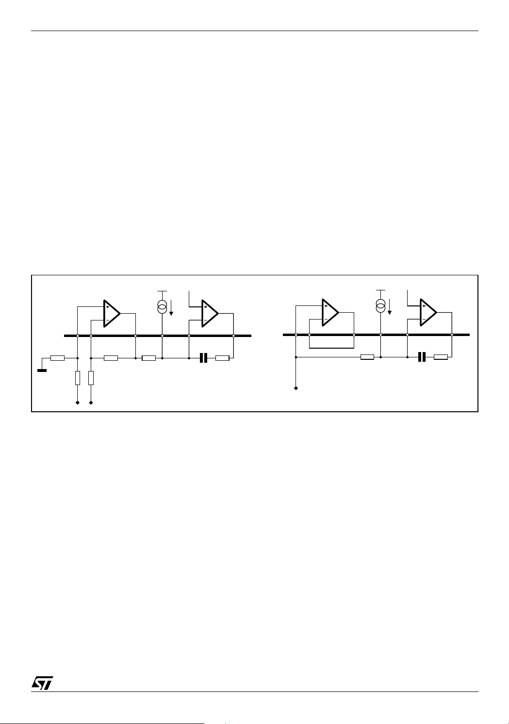
3.3 DRIVER SECTION
The integrated high-current drivers allow using different types of power MOS (also multiple MOS to reduce
the R
The drivers for the high-side mosfets use BOOTx pins for supply and PHASEx pins for return. The drivers
for the low-side mosfets use VCCDR pin for supply and PGND pin for return. A minimum voltage of 4.6V
at VCCDR pin is required to start operations of the device.
The controller embodies a sophisticated anti-shoot-through system to minimize low side body diode conduction time maintaining good efficiency saving the use of Schottky diodes in parallel to the LS mosfets.
The dead time is reduced to few nanoseconds assuring that high-side and low-side mosfets are never
switched on simultaneously: when the high-side mosfet turns off, the voltage on its source begins to fall;
when the voltage reaches 2V, the low-side mosfet gate drive is applied with 30ns delay. When the lowside mosfet turns off, the voltage at LGATEx pin is sensed. When it drops below 1V, the high-side mosfet
gate drive is applied with a delay of 30ns. If the current flowing in the inductor is negative, the source of
high-side mosfet will never drop. To allow the turning on of the low-side mosfet even in this case, a watchdog controller is enabled: if the source of the high-side mosfet don't drop for more than 240ns, the low side
mosfet is switched on so allowing the negative current of the inductor to recirculate. This mechanism allows the system to regulate even if the current is negative.
The BOOTx and VCCDR pins are separated from IC's power supply (VCC pin) as well as signal ground
(SGND pin) and power ground (PGND pin) in order to maximize the switching noise immunity. The separated supply for the different drivers gives high flexibility in mosfet choice, allowing the use of logic-level
mosfet. Several combination of supply can be chosen to optimize performance and efficiency of the application. Power conversion is also flexible; 5V or 12V bus can be chosen freely.
The peak current is shown for both the upper and the lower driver of the two phases in Figure 7. A 10nF
capacitive load has been used. For the upper drivers, the source current is 1.9A while the sink current is
1.5A with V
current is 2A with VCCDR = 12V.
), maintaining fast switching transition.
dsON
BOOT
-V
= 12V; similarly, for the lower drivers, the source current is 2.4A while the sink
PHASE
Figure 7. Drivers peak current: High Side (left) and Low Side (right)
CH3 = HGATE1; CH4 = HGATE2 CH3 = LGATE1; CH4 = LGATE2
3.4 CURRENT READING AND OVER CURRENT
The current flowing trough each phase is read using the voltage drop across the low side mosfets R
or across a sense resistor (R
) in series to the LS mosfet and internally converted into a current. The
SENSE
dsON
transconductance ratio is issued by the external resistor Rg placed outside the chip between ISENx and
PGNDSx pins toward the reading points. The differential current reading rejects noise and allows to place
sensing element in different locations without affecting the measurement's accuracy. The current reading
11/29
Page 12

L6712A L6712
x
E
circuitry reads the current during the time in which the low-side mosfet is on (OFF Time). During this time,
the reaction keeps the pin ISENx and PGNDSx at the same voltage while during the time in which the
reading circuitry is off, an internal clamp keeps these two pins at the same voltage sinking from the ISENx
pin the necessary current (Needed if low-side mosfet R
imum rating overcome on ISENx pin).
The proprietary current reading circuit allows a very precise and high bandwidth reading for both positive
and negative current. This circuit reproduces the current flowing through the sensing element using a high
speed Track & Hold transconductance amplifier. In particular, it reads the current during the second half
of the OFF time reducing noise injection into the device due to the mosfet turn-on (See Figure 8-left). Track
time must be at least 200ns to make proper reading of the delivered current.
This circuit sources a constant 50µA current from the PGNDSx pin: it must be connected through the Rg
resistor to the ground side of the sensing element (See Figure 8-right). The two current reading circuitries
use this pin as a reference keeping the ISENx pin to this voltage.
The current that flows in the ISENx pin is then given by the following equation:
sense is implemented to avoid absolute max-
dsON
R
SENSEIPHASEx
------------------------------------------------- 50µAI
Where R
I
ISENx
is an external sense resistor or the R
SENSE
50µA
ductance resistor used between ISENx and PGNDSx pins toward the reading points; I
⋅
R
g
of the low side mosfet and Rg is the transcon-
dsON
+=+=
INFOx
PHASEx
is the current
carried by the relative phase. The current information reproduced internally is represented by the second
term of the previous equation as follow:
I
INFOx
R
SENSEIPHASEx
-------------------------------------------------=
⋅
R
g
Since the current is read in differential mode, also negative current information is kept; this allow the device to check for dangerous returning current between the two phases assuring the complete equalization
between the phase's currents. From the current information of each phase, information about the total current delivered (I
taken. I
INFOX
FB
= I
INFO1
+I
INFO2
is then compared to I
) and the average current for each phase (I
to give the correction to the PWM output in order to equalize the
AVG
AVG
= (I
INFO1
+I
INFO2
)/2 ) is
current carried by the two phases.
Figure 8. Current reading timing (left) and circuit (right)
I
LS1
LGATEx
I
LS2
IFB
ISENx
PGNDSx
Rg
I
ISEN
Rg
SENSE
R
PHAS
I
Track & Hold
50µA
The transconductance resistor Rg can be designed in order to have current information of 25µA per phase
at full nominal load; the over current intervention threshold is set at 140% of the nominal (I
According to the above relationship, the over current threshold (I
) for each phase, which has to be
OCPx
INFOx
placed at 1/2 of the total delivered maximum current, results:
12/29
= 35µA).
Page 13

L6712A L6712
(
)
T
(
)
⋅
35µARg⋅
I
OCPx
---------------------------
R
SENSE
Rg
Since the device senses the output current across the low-side mosfets (or across a sense resistors in
series with them) the device limits the bottom of the inductor current triangular waveform: an over current
is detected when the current flowing into the sense element is greater than I
■ L6712 - Dynamic Maximum Duty Cycle Limitation
The maximum duty cycle is limited as a function of the measured current and, since the oscillator frequency is fixed once programmed, imply a maximum on-time limitation as follow (where T is the switching period T=1/f
T
ON,MAX
SW
and I
is the output current):
OUT
0.80 IFB– 5.73k⋅()T0.80
R
⎛⎞
⎝⎠
SENSE
--------------------- -
Rg
This linear dependence has a value at zero load of 0.80·T and at maximum current of 0.40·T typical and
results in two different behaviors of the device:
Figure 9. TON Limited Operation
I
OCPxRSENSE
------------------------------------------ -
5.73k⋅⋅–
I
OUT
35µA
⋅=⋅=
T =
==
(I
OCPx
INFOx
⎧
T 0.80 T I
⎪
⎨
T 0.40 T I
⎪
⎩
> 35µA).
FB
FB
0µA=⋅=
70µA=⋅=
V
0.80·V
0.40·V
OUT
IN
IN
TONLimited Output
characteristic
I
=2·I
OCP
OCPx
I
=70µA
DROOP
I
OUT
V
0.80·V
0.40·V
OU
IN
IN
Resulting Output
characteristic
Desired Output
characteristic and
UVP threshold
I
=2·I
OCPx
=70µA
OCP
I
DROOP
I
OUT
a) Maximum output Voltage b) TON Limited Output Voltage
T
Limited Output Voltage.
ON
This happens when the maximum ON time is reached before the current in each phase reaches I
< 35µA).
FOx
Figure 9a shows the maximum output voltage that the device is able to regulate considering the T
itation imposed by the previous relationship. If the desired output characteristic crosses the T
OCPx
limited
ON
ON
(I
IN-
lim-
maximum output voltage, the output resulting voltage will start to drop after crossing. In this case, the device doesn't perform constant current limitation but only limits the maximum duty cycle following the previous relationship. The output voltage follows the resulting characteristic (dotted in Figure 9b) until UVP is
detected or anyway until I
= 70µA.
FB
Constant Current Operation
This happens when ON time limitation is reached after the current in each phase reaches I
OCPx
(I
INFOx
>
35µA).
The device enters in Quasi-Constant-Current operation: the low-side mosfets stays ON until the current
read becomes lower than I
OCPx
(I
< 35µA) skipping clock cycles. The high side mosfets can be turned
INFOx
ON with a TON imposed by the control loop at the next available clock cycle and the device works in the
13/29
Page 14

L6712A L6712
usual way until another OCP event is detected.
This means that the average current delivered can slightly increase also in Over Current condition since
the current ripple increases. In fact, the ON time increases due to the OFF time rise because of the current
has to reach the I
When this happens, the device works in Constant Current and the output voltage decrease as the load
increase. Crossing the UVP threshold causes the device to reset.
Figure 10 shows this working condition.
It can be observed that the peak current (I
I
peakIOCPx
bottom. The worst-case condition is when the ON time reaches its maximum value.
OCPx
peak
VINVout
–
------------------------------------- -
min
L
) is greater than the I
Ton
MAXIOCPx
but it can be determined as follow:
OCPx
VINVout
–
-------------------------------------- -
MIN
L
0.40 T⋅⋅+=⋅+=
Where V
is the minimum output voltage (VID-40% as follow).
outMIN
The device works in Constant-Current, and the output voltage decreases as the load increase, until the
output voltage reaches the under-voltage threshold (Vout
MIN
).
The maximum average current during the Constant-Current behavior results:
I
MA X ,TOT
2I
MAX
⎛⎞
⋅=⋅=
2I
OCPx
⎝⎠
Ipeak I
------------------------------------- -+
–
2
OCPx
In this particular situation, the switching frequency results reduced. The ON time is the maximum allowed
(T
) while the OFF time depends on the application:
onMAX
–
T
OFF
Ipeak I
------------------------------------- -
L
V
OCPx
OUt
f
----------------------------------------- -=⋅=
T
1
ONmaxTOFF
+
Figure 10. Constant Current operation
Ipeak
I
MAX
I
OCPx
Vout
Droop effect
UVP
TonMAX
Over current is set anyway when I
a) Maximum current for each phase b) Output Characteristic
TonMAX
INFOx
to work with convenient values for I
(I
=50µA) 2·I
DROOP
OCPx (IDROOP
reaches 35µA (IFB=70µA). The full load value is only a convention
. Since the OCP intervention threshold is fixed, to modify the per-
FB
MAX,TOT
I
=70µA)
Iout
centage with respect to the load value, it can be simply considered that, for example, to have on OCP
threshold of 200%, this will correspond to I
spond to I
= 17.5µA (IFB = 35µA).
INFOx
= 35µA (IFB = 70µA). The full load current will then corre-
INFOx
Once the UVP threshold has been intercepted, the device resets with all power mosfets turned OFF. Another soft start is then performed allowing the device to recover from OCP once the over load cause has
been removed.
Crossing the UVP threshold causes the device to reset: all mosfets are turned off and a new soft start is
14/29
Page 15
L6712A L6712
then implemented allowing the device to recover if the over load cause has been removed.
■ L6712A - Fixed Maximum Duty Cycle Limitation
The maximum duty cycle is fixed and constant with the delivered current. The device works in constant
current operation once the OCP threshold has overcome. Refer to the above Constant Current section in
which only the different value in the maximum duty has to be considered as follow:
VINVout
I
peakIOCPx
–
------------------------------------- -
min
Ton
L
MAXIOCPx
All the above reported relationships about the deliverable current once in quasi-constant current and constant current are still valid in this case.
3.5 REMOTE SENSE AMPLIFIER
Remote Sense Amplifier is integrated in order to recover from losses across PCB traces and wiring in high
current DC/DC converter remote sense of the regulated voltage is required to maintain precision in the
regulation. The integrated amplifier is a low-offset error amplifier; external resistors are needed as shown
in Figure 11 to implement a differential remote sense amplifier.
Figure 11. Remote Sense Amplifier Connections
VINVout
–
-------------------------------------- -
MIN
L
0.85 T⋅⋅+=⋅+=
R2
Remote
V
Reference
REMOTE
AMPLIFIER
FBG
FBR
R1
R1
Remote
Ground
OUT
VSEN
R2
RB used RB Not Used
I
DROOP
R
FB
FB
DROOP
ERROR
AMPLIFIER
COMP
R
C
F
F
FBR
V
OUT
FBG
REMOTE
AMPLIFIER
VSEN
R
FB
DROOP
Reference
I
DROOP
FB
ERROR
AMPLIFIER
COMP
R
C
F
F
Equal resistors give to the resulting amplifier a unity gain: the programmed reference will be regulated
across the remote load.
To regulate output voltages different from the available references, the Remote Amplifier gain can be adjusted simply changing the value of the external resistors as follow (see Figure 11):
RA_Gain
----------------------------------------------------------------------------------------=
Remote_V
V
OUT
VSEN
Remote_GND–
R2
------- -=
R1
to regulate a voltage double of the reference, the above reported gain must be equal to ½.
Modifying the Remote Amplifier Gain (in particular with values higher than 1) allows also to regulate voltages lower than the programmed reference.
Since this Amplifier is connected as a differential amplifier, when calculating the offset introduced
in the regulated output voltage, the "native" offset of the amplifier must be multiplied by the term
K
= [1+(1/RA_Gain)] because a voltage generator insisting on the non-inverting input represents
OS
the offset.
If remote sense is not required, it is enough connecting RFB directly to the regulated voltage: VSEN becomes not connected and still senses the output voltage through the remote amplifier. In this case the use
of the external resistors R1 and R2 becomes optional and the Remote Sense Amplifier can simply be connected as a "buffer" to keep VSEN at the regulated voltage (See Figure 11). Avoiding use of Remote Amplifier saves its offset in the accuracy calculation but doesn't allow remote sensing.
15/29
Page 16

L6712A L6712
p
3.6 INTEGRATED DROOP FUNCTION (Optional)
Droop function realizes dependence between the regulated voltage and the delivered current (Load Regulation). In this way, a part of the drop due to the output capacitor ESR in the load transient is recovered.
As shown in Figure 12, the ESR drop is present in any case, but using the droop function the total deviation of the output voltage is minimized.
Connecting DROOP pin and FB pin together, forces a current I
into the feedback resistor R
implementing the load regulation dependence. If RA_Gain is the Remote
FB
Amplifier gain, the Output Characteristic is then given by the following relationship (when droop enabled):
, proportional to the output current,
DROOP
V
OUT
1
------------------------ -
RA_Gain
VID R
⋅–()⋅
FBIDROOP
1
------------------------ -
RA_Gain
⎛⎞
⋅==
VID R
⎝⎠
FB
R
SENSE
--------------------- -
⋅⋅–
Rg
I
OUT
with a remote amplifier gain of 1/2, the regulated output voltage results in being doubled.
The Droop current is equal to 50µA at nominal full load and 70µA at the OC intervention threshold, so the
maximum output voltage deviation is equal to:
1
∆V
FULL POSITIVE– LOAD–
-------------------------
RA_Gain
50µ A ∆V
R⋅
FB
OC INTERVENTION–
Droop function is provided only for positive load; if negative load is applied, and then I
1
-------------------------
RA _Gain
INFOx
70µ A⋅–=⋅–=
R⋅
FB
<0, no current
is sunk from the FB pin. The device regulates at the voltage programmed by the VID.
If this effect is not desired, shorting DROOP pin to SGND, the device regulates as a Voltage Mode Buck
converter.
Figure 12. Load Transient response (Left) and DROOP pin connection (Right).
V
MAX
V
NOM
V
MIN
DROOP PIN = GND
DROOP PIN = FB PIN
ESR DROP
R2
Remote
V
REMOTE
AMPLIFIER
FBG FBR
R1 R1
Remote
Ground
OUT
VSEN
R
FB
Short to GND if DROOP function is not
lemented (Classic Voltage Mode).
im
Reference
I
DROOP
FB COMP
DROOP
R2
C
F
ERROR
AMPLIFIER
R
F
3.7 MONITOR AND PROTECTIONS
The device monitors through pin VSEN the regulated voltage in order to build the PGOOD signal and manage the OVP / UVP conditions.
■ PGOOD. Power good output is forced low if the voltage sensed by VSEN is not within ±12% (Typ.) of
the programmed value (RA_Gain=1). It is an open drain output and it is enabled only after the soft start
is finished (2048 clock cycles after start-up). During Soft-Start this pin is forced low.
■ UVP. If the output voltage monitored by VSEN drops below the 60% of the reference voltage for more
than one clock period, the device turns off all mosfets and resets restarting operations with a new softstart phase (hiccup mode, see Figure 13).
■ OVP. Enabled once VCC crosses the turn-ON threshold: when the voltage monitored by VSEN reaches
115% (min) of the programmed voltage (or the external reference) the controller permanently switches
on both the low-side mosfets and switches off both the high-side mosfets in order to protect the load.
The OSC/ FAULT pin is driven high (5V) and power supply (VCC) turn off and on is required to restart
operations.
Both Over Voltage and Under Voltage are active also during soft start (Under Voltage after than the
16/29
Page 17

L6712A L6712
x
reference voltage reaches 0.6V). The reference used in this case to determine the UV thresholds is the
increasing voltage driven by the 2048 soft start digital counter while the reference used for the OV
threshold is the final reference programmed by the VID pins or available on the REF_IN/OUT pin.
Figure 13. UVP Protection & Hiccup Mode.
CH1=PGOOD; CH2=Vout; CH3=REF_OUT; CH4=Iout
3.8 SOFT START AND INHIBIT
At start-up a ramp is generated increasing the loop reference from 0V to the final value programmed by
VID in 2048 clock periods as shown in Figure 14.
Once the soft start begins, the reference is increased: upper and lower Mosfets begin to switch and the
output voltage starts to increase with closed loop regulation. At the end of the digital soft start, the Power
Good comparator is enabled and the PGOOD signal is then driven high (See Figure 14).
The Under Voltage comparator is enabled when the increasing reference voltage reaches 0.6V while OVP
comparator is always active with a threshold equal to the +15%_min of the final reference.
The Soft-Start will not take place, if both VCC and VCCDR pins are not above their own turn-on thresholds.
During normal operation, if any under-voltage is detected on one of the two supplies the device shuts
down. Forcing the OSC/INH pin to a voltage lower than 0.5V (Typ.) disables the device: all the power mosfets and protections are turned off until the condition is removed.
Figure 14. Soft Start.
VCC=V
CCDR
V
LGATE
V
PGOOD
OUT
Turn ON threshold
t
t
t
2048 Clock Cy cles
Timing Diagram Acquisition:
t
CH1=PGOOD; CH2=VOUT; CH3=REF_OUT
17/29
Page 18

L6712A L6712
3.9 INPUT CAPACITOR
The input capacitor is designed considering mainly the input RMS current that depends on the duty cycle
as reported in Figure 15. Considering the two-phase topology, the input RMS current is highly reduced
comparing with a single-phase operation.
It can be observed that the input RMS value is one half of the single-phase equivalent input current in the
worst case condition that happens for D=0.25 and D=0.75.
The power dissipated by the input capacitance is then equal to:
P
RMS
ESR I
⋅=
()
2
RMS
Input capacitor is designed in order to sustain the ripple relative to the maximum load duty cycle. To reach
the RMS value needed and also to minimize components cost, the input capacitance is realized by more
than one physical capacitor. The equivalent RMS current is simply the sum of the single capacitor's RMS
current.
Input bulk capacitor must be equally divided between high-side drain mosfets and placed as close as possible to reduce switching noise above all during load transient. Ceramic capacitor can also introduce benefits in high frequency noise de coupling, noise generated by parasitic components along power path.
Figure 15. Input RMS Current vs. Duty Cycle (D) and Driving Relationships.
)
OUT
/I
RMS
0.50
0.25
Rms Current Normalized (I
Duty Cycle (V
Single Phase
Dual Phase
0.50 0.75 0.25
OUT/VIN
)
I
rms
⎧
I
OUT
⎪
------------
⎪
=
⎨
I
⎪
------------
⎪
⎩
2
OUT
2
2D 1 2D–()⋅ if D < 0.5⋅
2D 1–()22D–()⋅ if D > 0.5⋅
Where D = V
OUT/VIN
3.10 OUTPUT CAPACITOR
The output capacitor is a basic component for the fast response of the power supply.
Two-phase topology reduces the amount of output capacitance needed because of faster load transient
response (switching frequency is doubled at the load connections). Current ripple cancellation due to the
180° phase shift between the two phases also reduces requirements on the output ESR to sustain a specified voltage ripple.
Moreover, if DROOP function is enabled, bigger ESR can be used still keeping the same transient tolerances. In fact, when a load transient is applied to the converter's output, for first few microseconds the
current to the load is supplied by the output capacitors. The controller recognizes immediately the load
transient and increases the duty cycle, but the current slope is limited by the inductor value.
The output voltage has a first drop due to the current variation inside the capacitor (neglecting the effect
of the ESL):
∆V
OUT
∆I
OUT
ESR⋅=
A minimum capacitor value is required to sustain the current during the load transient without discharge
18/29
Page 19

L6712A L6712
it. The voltage drop due to the output capacitor discharge is given by the following equation:
2
∆V
OUT
--------------------------------------------------------------------------------=
4C
∆I
OUTVIndmaxVOUT
OUT
L⋅
–⋅()⋅⋅
Where D
is the maximum duty cycle value. The lower is the ESR, the lower is the output drop during
MAX
load transient and the lower is the output voltage static ripple.
3.11 INDUCTOR DESIGN
The inductance value is defined by a compromise between the transient response time, the efficiency, the
cost and the size. The inductor has to be calculated to sustain the output and the input voltage variation
to maintain the ripple current ∆I
between 20% and 30% of the maximum output current. The inductance
L
value can be calculated with this relationship:
V
Where F
L
is the switching frequency, VIN is the input voltage and V
SW
fs ∆I
⋅
–
INVOUT
------------------------------
V
OUT
-------------- -
⋅=
V
L
IN
is the output voltage.
OUT
Increasing the value of the inductance reduces the ripple current but, at the same time, reduces the converter response time to a load transient. The response time is the time required by the inductor to change
its current from initial to final value. Since the inductor has not finished its charging time, the output current
is supplied by the output capacitors. Minimizing the response time can minimize the output capacitance
required.
The response time to a load transient is different for the application or the removal of the load: if during
the application of the load the inductor is charged by a voltage equal to the difference between the input
and the output voltage, during the removal it is discharged only by the output voltage. The following expressions give approximate response time for ∆I load transient in case of enough fast compensation network response:
t
application
L ∆I⋅
------------------------------
V
–
INVOUT
t
removal
L ∆I⋅
-------------- -
V
OUT
==
The worst condition depends on the input voltage available and the output voltage selected. Anyway the
worst case is the response time after removal of the load with the minimum output voltage programmed
and the maximum input voltage available.
3.12 MAIN CONTROL LOOP
The system control loop topology depends on the DROOP pin connection: if connected to FB (droop function active) an Average Current Mode topology must be considered while, if connected to GND (droop
function not active) a Voltage Mode topology must be considered instead.
Anyway, the system control loop encloses the Current Sharing control loop to allow proper sharing to the
inductor' currents. Each loop gives, with a proper gain, the correction to the PWMs in order to minimize
the error in its regulation: the Current Sharing control loop equalize the currents in the inductors while the
output voltage control loop fixes the output voltage equal to the reference programmed by VID (with or
without the droop effect and with or without considering the Remote Amplifier Gain). Figure 16 reports the
block diagram of the main control loop.
19/29
Page 20

L6712A L6712
Figure 16. Main Control Loop Diagram
+
+
PWM1
1/5
1/5
PWM2
ERROR
AMPLIFIER
4/5
CURRENT
SHARING
DUTY CYCLE
CORRECTION
REFERENCE
PROGRAMMED
+
-
BY VID
FBCOMP
I
INFO2
I
INFO1
L
1
L
2
C
O
RA_Gain
R
O
D03IN1518
Z
F(S)
R
FB
3.12.1Current Sharing (CS) Control Loop
Active current sharing is implemented using the information from Trans conductance differential amplifier.
A current reference equal to the average of the read current (I
) is internally built; the error between the
AVG
read current and this reference is converted to a voltage with a proper gain and it is used to adjust the duty
cycle whose dominant value is set by the error amplifier at COMP pin (See Figure 17).
The current sharing control is a high bandwidth control loop allowing current sharing even during load transients.
The current sharing error is affected by the choice of external components; choose precise Rg resistor
(±1% is necessary) to sense the current. The current sharing error is internally dominated by the voltage
offset of Trans conductance differential amplifier; considering a voltage offset equal to 2mV across the
sense resistor, the current reading error is given by the following equation:
∆I
READ
--------------------
I
MAX
2mV
--------------------------------------- -=
R
SENSEIMAX
⋅
Figure 17. Current Sharing Control Loop.
L
+
PWM1
1
20/29
COMP
I
1/5
1/5
+
PWM2
CURRENT
SHARING
DUTY CYCLE
CORRECTION
D02IN1393
INFO2
I
INFO1
L
2
V
OUT
Page 21

L6712A L6712
Where ∆I
For R
SENSE
and R
SENSE
is the difference between one phase current and the ideal current (I
READ
= 4mΩ and I
= 40A the current sharing error is equal to 2.5%, neglecting errors due to Rg
MAX
mismatches.
MAX
/2).
3.12.2Average Current Mode (ACM) Control Loop (DROOP=FB)
The average current mode control loop is reported in Figure 18. The current information I
the DROOP pin flows into R
implementing the dependence of the output voltage from the read current.
FB
DROOP
sourced by
The ACM control loop gain results (obtained opening the loop after the COMP pin):
G
LOOP
s()
PWM Z
----------------------------------------------------------------------------------------------------------------------- -–=
Z
P
s() R
F
DROOP
s() ZLs()+()
Z
F
-------------- - 1
As()
RA_Gain Z⋅Ps()+()⋅⋅
s()
1
⎛⎞
----------- -+
⎝⎠
As()
R
⋅+⋅
FB
Where:
Rsense
■ is the equivalent output resistance determined by the droop function;
R
DROOP
■ Z
(s) is the impedance resulting by the parallel of the output capacitor (and its ESR) and the applied
P
----------------------
Rg
⋅=
R
FB
load Ro;
■ Z
(s) is the compensation network impedance;
F
■ Z
(s) is the parallel of the two inductor impedance;
L
■ A(s) is the error amplifier gain;
V
4
IN
-------------------
■ is the ACM PWM transfer function where ∆V
PWM
-- -
⋅=
∆V
5
OSC
is the oscillator ramp amplitude
OSC
and has a typical value of 3V
■ RA_Gain is the Remote Amplifier Gain.
Removing the dependence from the Error Amplifier gain, so assuming this gain high enough, the control
loop gain results:
G
LOOP
s()
⋅⋅ ⋅–=
5
-------------------
∆V
OSC
------------------------------------
Z
V
4
IN
---
Considering now that in the application of interest it can be assumed that R
R
<<Ro, it results:
DROOP
G
LOOP
s()
4
---
5
V
IN
-------------------
∆V
OSC
s()
Z
F
-------------- -
R
FB
-------------------------------------------------------------------------------------------------------------------------------------------
2
s
Co
L
-- - s
2
s()
Z
F
s() ZLs()+
P
1sCo
--------------- Co ESR Co
2Ro⋅
RA_Gain Z⋅
⎛⎞
Rs
-------------------------------------------- -+
------- -
⎜⎟
Rg
⎝⎠
R
DROOP
⎛⎞
------------------------ - ESR+
⋅⋅+
⎝⎠
RA_Gain
R
L
s()
P
FB
>>RL; ESR<<Ro and
o
L
---------------
⋅+⋅+ 1+⋅+⋅⋅
2Ro⋅
RA_Gain⋅⋅⋅ ⋅–=
21/29
Page 22

L6712A L6712
ω
ωZ
ωLC
Figure 18. ACM Control Loop Gain Block Diagram (left) and Bode Diagram (right).
VCOMP
PWM
ZF
COMP
d•VIN
IDROOP
RF CF
L/2
Cout
ESR
FB
DROOP
RFB
RA_Gain
VID
VOUT
Rout
K
dB
G
LOOP
(s)
Z
F
ωT
⎡
V
4
K
IN
⎢
∆V
5
⎣
⎤
1
⋅⋅=
⎥
R
FBOSC
⎦
dB
The ACM control loop gain is designed to obtain a high DC gain to minimize static error and cross the 0dB
axes with a constant -20dB/dec slope with the desired crossover frequency ω
. Neglecting the effect of
T
ZF(s), the transfer function has one zero and two poles. Both the poles are fixed once the output filter is
designed and the zero is fixed by ESR and the Droop resistance.
To obtain the desired shape an R
at ω
=1/RFCF is then introduced together with an integrator. This integrator minimizes the static error
F
series network is considered for the ZF(s) implementation. A zero
F-CF
while placing the zero in correspondence with the L-C resonance a simple -20dB/dec shape of the gain is
assured (See Figure 18). In fact, considering the usual value for the output filter, the LC resonance results
to be at frequency lower than the above reported zero.Compensation network can be simply designed
placing ω
= ωLC and imposing the cross-over frequency ωT as desired obtaining:
Z
L
-- -
Co
⋅
2
------------------- -=⋅⋅ ⋅=
R
F
R
F
RFB∆V
⋅
---------------------------------- -
OSC
V
IN
5
-- -
4
----------------------------------------------------------
ω
T
⎛⎞
2
⋅
⎝⎠
L
R
DROOP
------------------------ - ESR+
RA_Gain
C
F
3.12.3Voltage Mode (VM) Control Loop (DROOP = SGND)
Disconnecting the DROOP pin from the Control Loop, the system topology becomes a Voltage Mode. The
simplest way to compensate this loop still keeping the same compensation network consists in placing the
RF-CF zero in correspondence with the L-C filter resonance.
The loop gain becomes now:
G
LOOP
s()
V
IN
------------------ -
V
∆
OSC
s()
Z
F
-------------- -
R
FB
s()
Z
P
------------------------------------
Z
s() ZLs()+
P
RA_Gain⋅⋅ ⋅–=
3.13 LAYOUT GUIDELINES
Since the device manages control functions and high-current drivers, layout is one of the most important
things to consider when designing such high current applications.
A good layout solution can generate a benefit in lowering power dissipation on the power paths, reducing
radiation and a proper connection between signal and power ground can optimize the performance of the
control loops.
22/29
Page 23

L6712A L6712
Integrated power drivers reduce components count and interconnections between control functions and
drivers, reducing the board space.
Here below are listed the main points to focus on when starting a new layout and rules are suggested for
a correct implementation.
■ Power Connections.
These are the connections where switching and continuous current flows from the input supply towards
the load. The first priority when placing components has to be reserved to this power section, minimizing
the length of each connection as much as possible.
To minimize noise and voltage spikes (EMI and losses) these interconnections must be a part of a power
plane and anyway realized by wide and thick copper traces.
Figure 19. Power connections and related connections layout guidelines (same for both phases).
HGATEx
PHASEx
LGATEx
PGNDx
HS
VIN
R
gate
L
C
LS
R
gate
D
C
IN
OUT
LOAD
PHASEx
SGND
BOOTx
VCC
C
BOOTx
+VCC
HS
VIN
L
C
LS
D
C
IN
C
VCC
OUT
LOAD
a. PCB power and ground planes areas b. PCB small signal components placement
The critical components, i.e. the power transistors, must be located as close as possible, together and to
the controller. Considering that the "electrical" components reported in figure are composed by more than
one "physical" component, a ground plane or "star" grounding connection is suggested to minimize effects
due to multiple connections.
Figure 19a shows the details of the power connections involved and the current loops. The input capacitance (C
), or at least a portion of the total capacitance needed, has to be placed close to the power sec-
IN
tion in order to eliminate the stray inductance generated by the copper traces. Low ESR and ESL
capacitors are required.
■ Power Connections Related.
Figure 19b shows some small signal components placement, and how and where to mix signal and power
ground planes. The distance from drivers and mosfet gates should be reduced as much as possible. Propagation delay times as well as for the voltage spikes generated by the distributed inductance along the
copper traces are so minimized.
In fact, the further the mosfet is from the device, the longer is the interconnecting gate trace and as a consequence, the higher are the voltage spikes corresponding to the gate PWM rising and falling signals.
Even if these spikes are clamped by inherent internal diodes, propagation delays, noise and potential
causes of instabilities are introduced jeopardizing good system behavior. One important consequence is
that the switching losses for the high side mosfet are significantly increased.
For this reason, it is suggested to have the device oriented with the driver side towards the mosfets and
the GATEx and PHASEx traces walking together toward the high side mosfet in order to minimize distance
(see Figure 20). In addition, since the PHASEx pin is the return path for the high side driver, this pin must
be connected directly to the High Side mosfet Source pin to have a proper driving for this mosfet. For the
LS mosfets, the return path is the PGND pin: it can be connected directly to the power ground plane (if
23/29
Page 24

L6712A L6712
(
(
implemented) or in the same way to the LS mosfets Source pin. GATEx and PHASEx connections (and
also PGND when no power ground plane is implemented) must also be designed to handle current peaks
in excess of 2A (30 mils wide is suggested).
Gate resistors of few ohms help in reducing the power dissipated by the IC without compromising the system efficiency.
The placement of other components is also important:
– The bootstrap capacitor must be placed as close as possible to the BOOTx and PHASEx pins to min-
imize the loop that is created.
– Decoupling capacitor from VCC and SGND placed as close as possible to the involved pins.
– Decoupling capacitor from VCCDR and PGND placed as close as possible to those pins. This capac-
itor sustains the peak currents requested by the low-side mosfet drivers.
– Refer to SGND all the sensible components such as frequency set-up resistor (when present) and
Remote Amplifier Divider.
– Connect SGND to PGND plane on a single point to improve noise immunity. Connect at the load side
(output capacitor) if Remote Sense is not implemented to avoid undesirable load regulation effect.
– An additional 100nF ceramic capacitor is suggested to place near HS mosfet drain. This helps in re-
ducing noise.
– PHASE pin spikes. Since the HS mosfet switches in hard mode, heavy voltage spikes can be ob-
served on the PHASE pins. If these voltage spikes overcome the max breakdown voltage of the pin,
the device can absorb energy and it can cause damages. The voltage spikes must be limited by prop-
er layout, the use of gate resistors, Schottky diodes in parallel to the low side mosfets and/or snubber
network on the low side mosfets, to a value lower than 26V, for 20ns, at F
– Boot Capacitor Extra Charge. Systems that do not use Schottky diodes in parallel to the LS mosfet
might show big negative spikes on the phase pin. This spike can be limited as well as the positive
spike but has an additional consequence: it causes the bootstrap capacitor to be over-charged. This
extra-charge can cause, in the worst case condition of maximum input voltage and during particular
transients, that boot-to-phase voltage overcomes the abs. max. ratings also causing device failures.
It is then suggested in this cases to limit this extra-charge by:
– adding a small resistor in series to the boot diode (one resistor can be enough for all the diodes if
placed upstream the diode anode)
– using low capacitance diodes.
of 600kHz max.
SW
Figure 20. Device orientation (left) and sense nets routing (right).
To LS mosfet
or sense resistor)
To LS mosfet
or sense resistor)
To regula ted out put
ST L6917
■ Sense Connections.
Towards HS mosfet
(30 mils wide)
Towards LS mosfet
(30 mils wide)
Towards HS mosfet
(30 mils wide)
Remote Amplifier: Place the external resistors near the device to minimize noise injection and refer to
SGND. The connections for these resistors (from the remote load) must be routed as parallel nets in order
to compensate losses along the output power traces and also to avoid the pick-up of any noise. Connecting these pins in points far from the load will cause a non-optimum load regulation, increasing output tol-
24/29
Page 25

L6712A L6712
erance.
Current Reading: The Rg resistor has to be placed as close as possible to the ISENx and PGNDSx pins
in order to limit the noise injection into the device. The PCB traces connecting these resistors to the reading point must be routed as parallel traces in order to avoid the pick-up of any noise. It's also important to
avoid any offset in the measurement and to get a better precision, to connect the traces as close as possible to the sensing elements, dedicated current sense resistor or low side mosfet R
Moreover, when using the low side mosfet R
as current sense element, the ISENx pin is practically
dsON
connected to the PHASEx pin. DO NOT CONNECT THE PINS TOGETHER AND THEN TO THE HS
SOURCE! The device won't work properly because of the noise generated by the return of the high side
driver. In this case route two separate nets: connect the PHASEx pin to the HS Source (route together
with HGATEx) with a wide net (30 mils) and the ISENx pin to the LS Drain (route together with PGNDSx).
Moreover, the PGNDSx pin is always connected, through the Rg resistor, to the PGND: DO NOT CONNECT DIRECTLY TO THE PGND! In this case the device won't work properly. Route anyway to the LS
mosfet source (together with ISENx net).
Right and wrong connections are reported in Figure 21.
Symmetrical layout is also suggested to avoid any unbalance between the two phases of the converter.
Figure 21. PCB layout connections for sense nets.
NOT CORRECT CORRECT
VIA to GND plane
To PHASE
connection
.
dsON
To LS Drain
and Source
To HS Gate
and Source
Wrong (left) and correct (right) connections for the current reading sensing nets.
25/29
Page 26

L6712A L6712
4 Package informations
Figure 22. SO-28 Mechanical Data & Package Dimensions
DIM.
A 2.65 0.104
a1 0.1 0.3 0.004 0.012
b 0.35 0.49 0.014 0.019
b1 0.23 0.32 0.009 0.013
C 0.5 0.020
c1 45° (typ.)
D 17.7 18.1 0.697 0.713
E 10 10.65 0.394 0.419
e 1.27 0.050
e3 16.51 0.65
F 7.4 7.6 0.291 0.299
L 0.4 1.27 0.016 0.050
S8
mm inch
MIN. TYP. MAX. MIN. TYP. MAX.
(max.)
°
OUTLINE AND
MECHANICAL DATA
SO-28
26/29
Page 27

Figure 23. VFQFPN-36 Mechanical Data & Package Dimensions
L6712A L6712
mm inch
DIM.
MIN. TYP. MAX. MIN. TYP. MAX.
A 0.800 0.900 1.000 0.031 0.035 0.039
A1 0.020 0.050 0.0008 0.0019
A2 0.650 1.000 0.025 0.039
A3 0.250 0.01
b 0.180 0.230 0.300 0.007 0.009 0.012
D 5.875 6.000 6.125 0.231 0.236 0.241
D2 1.750 3.700 4.250 0.069 0.146 0.167
E 5.875 6.000 6.125 0.231 0.236 0.241
E2 1.750 3.700 4.250 0.069 0.146 0.167
e 0.450 0.500 0.550 0.018 0.020 0.022
L 0.350 0.550 0.750 0.014 0.022 0.029
ddd 0.080 0.003
OUTLINE AND
MECHANICAL DATA
VFQFPN-36 (6x6x1.0mm)
Very Fine Quad Flat Package No lead
7185332 F
27/29
Page 28

L6712A L6712
5 Revision History
Table 7. Revision History
Date Revision Description of Changes
March 2004 2 First Issue in EDOCS.
June 2005 3 Changed look and feel.
Inserted “Boot Capacitor Extra Charge” paragraph to page 27.
28/29
Page 29

L6712A L6712
Information furnished is believed to be accurate and reliable. However, STMicroelectronics assumes no responsibility for the consequences
of use of such information nor for any infringement of patents or other rights of third parties which may result from its use. No license is granted
by implication or otherwise under any patent or patent rights of STMicroelectronics. Specifications mentioned in this publication are subject
to change without notice. This publication supersedes and replaces all information previously supplied. STMicroelectronics products are not
authorized for use as critical components in life support devices or systems without express written approval of STMicroelectronics.
The ST logo is a registered trademark of STMicroelectronics.
All other names are the property of their respective owners
© 2005 STMicroelectronics - All rights reserved
Australia - Belgium - Brazil - Canada - China - Czech Republic - Finland - France - Germany - Hong Kong - India - Israel - Italy - Japan -
Malaysia - Malta - Morocco - Singapore - Spain - Sweden - Switzerland - United Kingdom - United States of America
STMicroelectronics group of companies
www.st.com
29/29
 Loading...