

Enhanced high voltage resonant controller
3/.
Features
■ Symmetrical duty cycle, variable frequency
control of resonant half bridge
■ Self-adjusting adaptive deadtime
■ High-accuracy oscillator
■ 2-level OCP: frequency-shift and immediate
shutdown
■ Interface with PFC controller
■ Anti-capacitive-mode protection
■ Burst-mode operation at light load
■ Input for brownout protection or power-on/off
sequencing
■ “Safe-start” procedure prevents hard switching
at startup
■ 600 V rail compatible high-side gate driver with
integrated bootstrap diode and high dv/dt
immunity
■ -300/800 mA high-side and low-side gate
drivers with UVLO pull-down
■ SO16N package
L6699
Datasheet − production data
Applications
■ SMPS for LCD TVs, desktop and AIO PCs,
servers, Telecom power
■ AC-DC adapter, open frame SMPS
Table 1. Device summary
Order codes Package Packing
L6699D
SO16N
L6699DTR Tape and reel
Tube
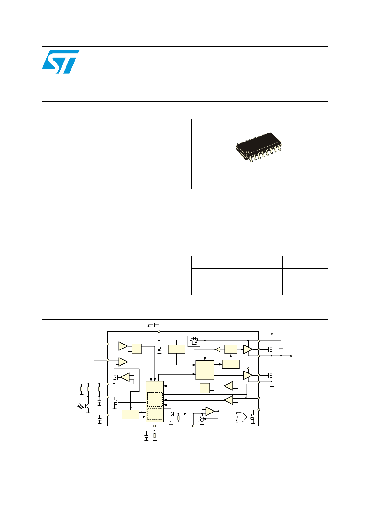
Figure 1. Block diagram
9FF
',
67%<
5)PLQ
&VV
&)
',6$%/(
6
64
9
9
,IPLQ
5
89/2
67$1'%<
9
9&2
',6
&21752/
&$3$&,7,9(
'(7(&7,21
67$57 83
/2*
02'(
6$)(
9
,&
'(/$<
89
'(7(&7,21
89/2
,6(1B',6
=(52&5266,1*'(7(&7,21
2&3
/,1(B2.
9
9
$
%22
('*(
6(16,1*
'5,9,1 *
/2*,&
$'$37,9(
'($'7,0(
46
/,1(
6<1&+5
7675 $3 ' ,2 '(
:, 7+
5
21286
89/2
'5,9(5
6+,)7(5
/9*
,6(1B',6
67$1'%<
+9*
/(9(/
'5,9(5
',6
9FF
9
9
April 2012 Doc ID 022835 Rev 1 1/38
This is information on a product in full production.
9
%227
+9*
287
/9*
*1'
,6(1
3)&B6723
+9
&
%227
/&7$1.
&,5&8, 7
!-V
www.st.com
38

Contents L6699
Contents
1 Description . . . . . . . . . . . . . . . . . . . . . . . . . . . . . . . . . . . . . . . . . . . . . . . . . 4
2 Electrical ratings . . . . . . . . . . . . . . . . . . . . . . . . . . . . . . . . . . . . . . . . . . . . 5
3 Thermal data . . . . . . . . . . . . . . . . . . . . . . . . . . . . . . . . . . . . . . . . . . . . . . . 5
4 Pin connections . . . . . . . . . . . . . . . . . . . . . . . . . . . . . . . . . . . . . . . . . . . . . 6
5 Electrical data . . . . . . . . . . . . . . . . . . . . . . . . . . . . . . . . . . . . . . . . . . . . . . 9
6 Application information . . . . . . . . . . . . . . . . . . . . . . . . . . . . . . . . . . . . . 12
6.1 Oscillator . . . . . . . . . . . . . . . . . . . . . . . . . . . . . . . . . . . . . . . . . . . . . . . . . 13
6.2 Adaptive deadtime . . . . . . . . . . . . . . . . . . . . . . . . . . . . . . . . . . . . . . . . . . 15
6.3 Safe-start procedure . . . . . . . . . . . . . . . . . . . . . . . . . . . . . . . . . . . . . . . . 17
7 Operation at no load or very light load . . . . . . . . . . . . . . . . . . . . . . . . . 21
8 Current sensing, OCP and OLP . . . . . . . . . . . . . . . . . . . . . . . . . . . . . . . 24
9 Capacitive-mode detection function . . . . . . . . . . . . . . . . . . . . . . . . . . . 28
10 Line sensing function . . . . . . . . . . . . . . . . . . . . . . . . . . . . . . . . . . . . . . . 30
11 Latched shutdown . . . . . . . . . . . . . . . . . . . . . . . . . . . . . . . . . . . . . . . . . . 32
12 Bootstrap section . . . . . . . . . . . . . . . . . . . . . . . . . . . . . . . . . . . . . . . . . . 32
13 Package information . . . . . . . . . . . . . . . . . . . . . . . . . . . . . . . . . . . . . . . . 34
14 Revision history . . . . . . . . . . . . . . . . . . . . . . . . . . . . . . . . . . . . . . . . . . . 37
2/38 Doc ID 022835 Rev 1

L6699 List of figures
List of figures
Figure 1. Block diagram . . . . . . . . . . . . . . . . . . . . . . . . . . . . . . . . . . . . . . . . . . . . . . . . . . . . . . . . . . . . 1
Figure 2. Pin connections (top view) . . . . . . . . . . . . . . . . . . . . . . . . . . . . . . . . . . . . . . . . . . . . . . . . . . 6
Figure 3. Typical system block diagram. . . . . . . . . . . . . . . . . . . . . . . . . . . . . . . . . . . . . . . . . . . . . . . . 8
Figure 4. Multimode operation of the L6699 . . . . . . . . . . . . . . . . . . . . . . . . . . . . . . . . . . . . . . . . . . . 12
Figure 5. Oscillator's internal block diagram . . . . . . . . . . . . . . . . . . . . . . . . . . . . . . . . . . . . . . . . . . . 13
Figure 6. Oscillator waveforms and their relationship with gate-driving signals. . . . . . . . . . . . . . . . . 14
Figure 7. Adaptive deadtime: principle schematic . . . . . . . . . . . . . . . . . . . . . . . . . . . . . . . . . . . . . . . 16
Figure 8. Relevant timing diagrams . . . . . . . . . . . . . . . . . . . . . . . . . . . . . . . . . . . . . . . . . . . . . . . . . . 16
Figure 9. Detailed view of deadtime during low-to-high transition of half bridge midpoint . . . . . . . . . 16
Figure 10. Comparison startup behavior: traditional controller (left), with L6699 (right) . . . . . . . . . . . 18
Figure 11. Comparison of initial cycles after startup: traditional controller (left), with L6699 (right). . . 19
Figure 12. Soft-start circuit . . . . . . . . . . . . . . . . . . . . . . . . . . . . . . . . . . . . . . . . . . . . . . . . . . . . . . . . . . 20
Figure 13. Input impedance vs. frequency curve in an LLC resonant half bridge . . . . . . . . . . . . . . . . 20
Figure 14. Narrow input voltage range. . . . . . . . . . . . . . . . . . . . . . . . . . . . . . . . . . . . . . . . . . . . . . . . . 21
Figure 15. Wide input voltage range . . . . . . . . . . . . . . . . . . . . . . . . . . . . . . . . . . . . . . . . . . . . . . . . . . 21
Figure 16. Load-dependent operating modes: timing diagram . . . . . . . . . . . . . . . . . . . . . . . . . . . . . . 22
Figure 17. How the L6699 can switch off a PFC controller at light load . . . . . . . . . . . . . . . . . . . . . . . 23
Figure 18. Current sensing techniques with sense resistor . . . . . . . . . . . . . . . . . . . . . . . . . . . . . . . . . 24
Figure 19. Current sensing techniques “lossless”, with capacitive shunt. . . . . . . . . . . . . . . . . . . . . . . 24
Figure 20. Soft-start and delayed shutdown upon overcurrent timing diagram
(safe-start details are not shown) . . . . . . . . . . . . . . . . . . . . . . . . . . . . . . . . . . . . . . . . . . . . 27
Figure 21. Details of hard-switching transition during capacitive-mode operation. . . . . . . . . . . . . . . . 28
Figure 22. Line sensing function: internal block diagram and timing diagram . . . . . . . . . . . . . . . . . . . 31
Figure 23. Bootstrap supply: standard circuit. . . . . . . . . . . . . . . . . . . . . . . . . . . . . . . . . . . . . . . . . . . . 33
Figure 24. Bootstrap supply: internal bootstrap synchronous diode . . . . . . . . . . . . . . . . . . . . . . . . . . 33
Figure 25. SO16N dimensions . . . . . . . . . . . . . . . . . . . . . . . . . . . . . . . . . . . . . . . . . . . . . . . . . . . . . . . 34
Figure 26. Package drawing . . . . . . . . . . . . . . . . . . . . . . . . . . . . . . . . . . . . . . . . . . . . . . . . . . . . . . . . 35
Figure 27. Recommended footprint (dimensions are in mm) . . . . . . . . . . . . . . . . . . . . . . . . . . . . . . . . 36
Doc ID 022835 Rev 1 3/38

Description L6699
1 Description
The L6699 is a double-ended controller specific to series-resonant half bridge topology.
Both LLC and LCC configurations are supported. It provides symmetrical complementary
duty cycle: the high-side switch and the low-side switch are driven ON/OFF 180° out-of-
phase for exactly the same time. Output voltage regulation is obtained by modulating the
operating frequency. The deadtime inserted between the turn-off of one switch and the turn-
on of the other one is automatically adjusted to best fit the transition times of the half bridge
midpoint. To drive the high-side switch with the bootstrap approach, the IC incorporates a
high voltage floating structure able to withstand more than 600 V with a synchronous-driven
high voltage DMOS that replaces the external fast-recovery bootstrap diode.
The IC enables the user to set the operating frequency range of the converter by means of a
high-accuracy externally programmable oscillator.
At startup, in addition to the traditional frequency-shift soft-start (the switching frequency
starts from a preset maximum value and then decays as far as the steady-state value
determined by the control loop), a proprietary circuit controls the half bridge to prevent hard-
switching from occurring in the initial cycles because of the unbalance in the V·s applied to
the transformer.
At light load the IC can be forced to enter a controlled burst-mode operation that keeps the
converter input consumption as low as possible.
IC protection functions include a current sense input for OCP with frequency shift and
delayed shutdown with automatic restart. Fast shutdown with automatic restart occurs if this
first-level protection cannot control the primary current. Additionally, the IC prevents the
converter from working in or too close to the capacitive mode, to guarantee soft-switching. A
latched disable input (DIS) can be used to implement OTP and/or OVP. The combination of
these protection features offers the highest degree of safety.
Other functions include a not-latched active-low disable input with current hysteresis, useful
for power sequencing or for brownout protection, and an interface with the PFC controller
that enables the switching-off of the pre-regulator during fault conditions or during burst-
mode operation.
4/38 Doc ID 022835 Rev 1

L6699 Electrical ratings
2 Electrical ratings
Table 2. Absolute maximum ratings
Symbol Pin Parameter Value Unit
V
BOOT
V
OUT
dV
OUT
V
CC
V
PFC_STOP
I
PFC_STOP
V
LINEmax
I
RFmin
V
ISEN
/dt 14 Floating ground max. slew rate 50 V/ns
16 Floating supply voltage (I
14 Floating ground voltage -3 to V
12 IC supply voltage (Icc ≤ 25 mA) Self-limited V
9 Maximum voltage (pin open) -0.3 to V
9 Maximum sink current (pin low) Self-limited A
7 Maximum pin voltage (Ipin ≤ 1 mA) Self-limited V
4 Maximum source current 2 mA
6 Current sense voltage -3 to 5 V
--- 1 to 5, 8 Analog inputs & outputs voltage -0.3 to 5 V
T
j
T
stg
--- Junction temperature operating range -40 to 150 °C
--- Storage temperature -55 to 150 °C
3 Thermal data
Table 3. Thermal data
≤ 5µA) -1 to 618 V
leak
BOOT
CC
V
V
Symbol Parameter Value Unit
R
th j-amb
P
tot
Max. thermal resistance, junction-to-ambient (SO16N) 120 °C/W
Power dissipation @tamb = 50 °C (SO16N) 0.83 W
Doc ID 022835 Rev 1 5/38

Pin connections L6699
4 Pin connections
Figure 2. Pin connections (top view)
&VV
'(/$<
&)
5)PLQ
67%<
,6(1
/,1(
',6
Table 4. Pin functions
N. Name Function
Soft-start. This pin connects an external capacitor to GND and a resistor to
(pin 4) that set both the initial oscillator frequency and the time constant
RF
min
for the frequency shift that occurs as the chip starts up (soft-start). An internal
1
2DELAY
C
SS
switch discharges this capacitor every time the chip turns off (VCC < UVLO,
LINE < 1.25 V, DIS > 1.85 V, ISEN > 1.5 V, DELAY > 2 V) to make sure it is softstarted next. Additionally the switch is activated when the voltage on the current
sense pin (ISEN) exceeds 0.8 V or when the converter is working too close to,
or in, the capacitive-mode operation.
Delayed shutdown upon overcurrent. A capacitor and a resistor are connected
from this pin to GND to set both the maximum duration of an overcurrent
condition before the IC stops switching and the delay after which the IC restarts
switching. Every time the voltage on the ISEN pin exceeds 0.8 V the capacitor
is charged by 350 µA current pulses and is slowly discharged by the external
resistor. If the voltage on the DELAY pin reaches 2 V, the soft-start capacitor is
completely discharged so that the switching frequency is pushed to its
maximum value and the 350 µA current source is kept always on. As the
voltage on the DELAY pin exceeds 3.5 V the IC stops switching and the internal
generator is turned off, so that the voltage on the pin decays because of the
external resistor. The IC is soft-restarted as the voltage drops below 0.3 V. In
this way, under short-circuit conditions, the converter works intermittently with
very low input average power.
If the voltage on the ISEN pin exceeds 1.5 V, the L6699 is immediately stopped
and the 350 µA current source is kept on until the voltage on the DELAY pin
reaches 3.5 V. Then, the generator is turned off and the voltage on the pin
decays because of the external resistor. Also in this case the IC is soft-restarted
as the voltage drops below 0.3 V.
9%227
+9*
287
1&
9FF
/9*
*1'
3)&B6723
!-V
Timing capacitor. A capacitor connected from this pin to GND is charged and
3CF
6/38 Doc ID 022835 Rev 1
discharged by internal current generators programmed by the external network
connected to pin 4 (RF
converter.
) and determines the switching frequency of the
min

L6699 Pin connections
Table 4. Pin functions (continued)
N. Name Function
Minimum oscillator frequency setting. This pin provides an accurate 2 V
reference, and a resistor connected from this pin to GND defines a current that
is used to set the minimum oscillator frequency. To close the feedback loop that
regulates the converter output voltage by modulating the oscillator frequency,
4RF
min
5STBY
6 ISEN
the phototransistor of an optocoupler is connected to this pin through a resistor.
The value of this resistor sets the maximum operating frequency. Initial
operating frequency should be set below 300 kHz; it is recommended not to
exceed such limit. An R-C series connected from this pin to GND sets
frequency shift at startup to prevent excessive energy inrush (soft-start).
Burst-mode operation threshold. The pin senses some voltage related to the
feedback control, which is compared to an internal reference (1.26 V). If the
voltage on the pin is lower than the reference, the IC enters an idle state and its
quiescent current is reduced. The chip restarts switching as the voltage
exceeds the reference by 30 mV. Soft-start is not invoked. This function realizes
burst-mode operation when the load falls below a level that can be programmed
by properly choosing the resistor connecting the optocoupler to the RF
Figure 1: Block diagram
(see
). Tie the pin to RF
if burst-mode is not used.
min
min
pin
Current sense input. The pin senses the instantaneous primary current though
a sense resistor or a capacitive divider for lossless sensing. If the voltage
exceeds a 0.8 V threshold the soft-start capacitor connected to pin 1 is
internally discharged: the frequency increases and so limits the power
throughput. Under output short-circuit, this normally results in a nearly constant
peak primary current. This condition is allowed for a maximum time set at pin 2.
If the current keeps on building up despite this frequency increase, a second
comparator referenced to 1.5 V disables switching immediately and activates a
restart delay procedure (see DELAY pin description for more information).
This pin is used also for capacitive-mode operation detection and for hardswitching prevention at startup. Do not short the pin to ground; this would
prevent the device from operating correctly.
Line sensing input. The pin is to be connected to the high voltage input bus with
a resistor divider to perform either AC or DC (in systems with PFC) brownout
protection. A voltage below 1.25 V shuts down the IC, lowers its consumption
and discharges the soft-start capacitor. IC operation is enabled as the voltage
7LINE
exceeds 1.25 V. The comparator is provided with current hysteresis: an internal
13 µA current generator is ON as long as the voltage applied at the pin is below
1.25 V, and is OFF if this value is exceeded. Bypass the pin with a capacitor to
GND to reduce noise pick-up. The voltage on the pin is top-limited by an
internal Zener. Tie the pin to V
Latched device shutdown. Internally, the pin connects a comparator that, when
the voltage on the pin exceeds 1.85 V, shuts the IC down and brings its
8DIS
consumption almost to a “before startup” level. The information is latched and it
is necessary to recycle the supply voltage of the IC to enable it to restart: the
latch is removed as the voltage on the V
Tie the pin to GND if the function is not used.
Open-drain ON/OFF control of PFC controller. This pin, normally open, is
intended for stopping the PFC controller, for protection purposes or during
burst-mode operation. It goes low when the IC is shut down by DIS > 1.85 V,
9PFC_STOP
ISEN > 1.5 V and STBY < 1.25 V. The pin is pulled low also when capacitive
mode operation is detected and when the voltage on the DELAY pin exceeds 2
V. In this latter case it goes back open as the voltage falls below 0.3 V. During
UVLO, it is open. Leave the pin unconnected if not used.
with a =100 kΩ resistor if not used.
CC
pin goes below the UVLO threshold.
CC
Doc ID 022835 Rev 1 7/38
Pin connections L6699
Table 4. Pin functions (continued)
N. Name Function
Chip ground. Current return for both the low-side gate-drive current and the
10 GND
11 LVG
12 V
CC
13 N.C.
14 OUT
15 HVG
16 V
BOOT
bias current of the IC. All of the ground connections of the bias components
should be tied to a track going to this pin and kept separate from any pulsed
current return.
Low-side gate-drive output. The driver is capable of 0.3 A min. source and 0.8 A
min. sink peak current to drive the lower MOSFET of the half bridge leg. The pin
is actively pulled to GND during UVLO.
Supply voltage of both the signal part of the IC and the low-side gate driver.
Sometimes a small bypass capacitor (0.1 µF typ.) to GND may be useful to
obtain a clean bias voltage for the signal part of the IC.
High voltage spacer. The pin is not internally connected to isolate the high
voltage pin and ease compliance with safety regulations (creepage distance) on
the PCB.
High-side gate-drive floating ground. Current return for the high-side gate-drive
current. Lay out the connection of this pin carefully to avoid too large spikes
below ground.
High-side floating gate-drive output. The driver is capable of 0.3 A min. source
and 0.8 A min. sink peak current to drive the upper MOSFET of the half bridge
leg. A resistor internally connected to pin 14 (OUT) ensures that the pin is not
floating during UVLO.
High-side gate-drive floating supply voltage. The bootstrap capacitor connected
between this pin and pin 14 (OUT) is fed by an internal synchronous bootstrap
diode driven in-phase with the low-side gate-drive. This patented structure
replaces the normally used external diode.
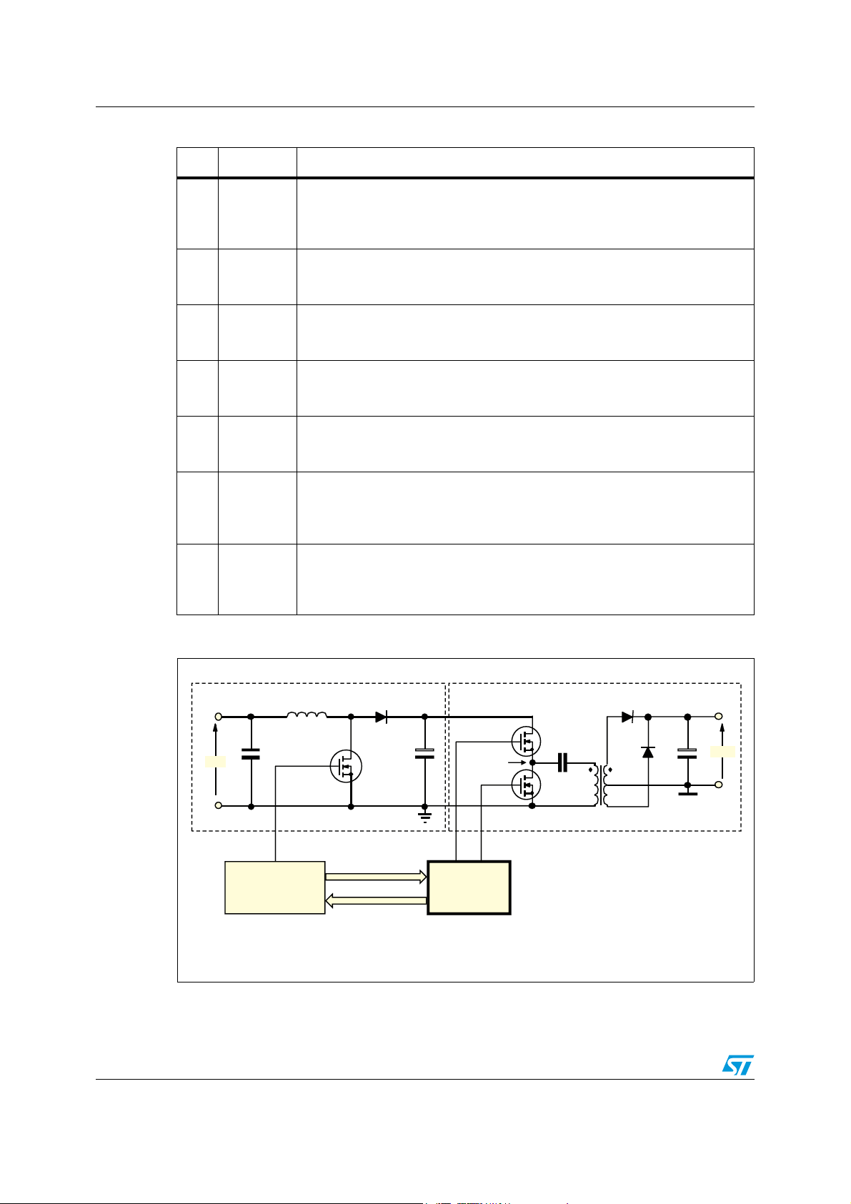
Figure 3. Typical system block diagram
0%2%'5,!4/2/04)/.!, 2%3/.!.4(!,&"2)$' %
INAC
6
, !,
, ,
2ES ON A N T ( "I S T UR N E D O FF I NC A S EO F
0&#gSANO MALOUSOPERATIONFORSAFETY
3(
4(
,
0&#CANBETURNEDOFFATLIGHT
L O AD TO EAS EC O MPLIAN C EW I T H
ENER GYSAVINGREGULATIONS
(!,&"2)$'%
-)$0/).4
,
TDC
OU
6
!-V
8/38 Doc ID 022835 Rev 1

L6699 Electrical data
5 Electrical data
Tj = -25 to +125 °C, VCC = 15 V, V
= 12 KΩ; unless otherwise specified.
RF
min
BOOT
= 15 V, C
HVG
= C
= 1 nF; CF = 470 pF;
LVG
Table 5. Electrical characteristics
Symbol Parameter Test condition Min. Typ. Max. Unit
Ic supply voltage
V
CC
V
CCOn
V
CCOff
Hys Hysteresis 2.55 V
V
Supply current
I
start-up
I
q
I
op
I
q
High-side floating gate-drive supply
R
DS(on)
Operating range After device turn-on 8.85 16 V
Turn-on threshold Voltage rising 10 10.7 11.4 V
Turn-off threshold Voltage falling 7.45 8.15 8.85 V
VCC clamp voltage Iclamp = 15 mA 16 17 17.9 V
Z
Startup current
Quiescent current Device on, V
Operating current Device on, V
Residual consumption
Synchronous bootstrap diode
ON-resistance
Before device turn-on
VCC = V
>1.92 V or V
V
DIS
<1.2 V
V
LINE
= high 150
V
LVG
CCOn
- 0.2 V
= 1 V 1 1.3 mA
STBY
= V
STBY
DELAY
RFmin
>3.65 V or
250 300 µA
34.1mA
400 500 µA
Overcurrent comparator
I
ISEN
V
ISENx
V
ISENdis
Input bias current V
Frequency shift threshold Voltage rising
Immediate stop threshold Voltage rising
Line sensing
V
V
LINE
I
Hys
clamp
Threshold voltage Voltage rising or falling
Current hysteresis V
Clamp level I
Latched disable function
V
I
DIS
DIS
Input bias current V
Disable threshold Voltage rising
Oscillator
f
osc
Oscillation frequency
= 0 to V
ISEN
= 1.2 V 101316µA
LINE
= 1 mA 6 V
LINE
= 0 to 1.92 V -1 µA
DIS
ISENdis
(1)
(1)
(1)
(1)
0.76 0.80 0.84 V
1.43 1.5 1.55 V
1.18 1.22 1.26 V
1.78 1.85 1.92 V
-1 µA
58.2 60 61.8
kHz
R
= 2.7 kΩ 225 235 245
RFmin
Doc ID 022835 Rev 1 9/38

Electrical data L6699
Table 5. Electrical characteristics (continued)
Symbol Parameter Test condition Min. Typ. Max. Unit
T
V
V
V
RF
D
CFp
CFv
REF
K
Deadtime self-adjustment
(2)
range
Peak value 3.9 V
Valley value 0.9 V
Voltage reference on pin 4
Current mirroring ratio 1 A/A
M
Timing resistor range 1 100 kΩ
min
Minimum value 0.23
Maximum
(1)
I
REF
value 0.7
= -2 mA
(1)
1.93 2 2.07
1.8 2 2.07
Zero-current comparator
V
ZCD neg
V
ZCD pos
Threshold voltage (-) -10 mV
Threshold voltage (+) +10 mV
Pfc_stop function
I
leak
R
PFC_STOP
High level leakage current V
ON-state resistance I
PFC_STOP
PFC_STOP
= VCC, V
= 1 mA, V
= 0 V 1 µA
DIS
> 1.92 V 130 200 Ω
DIS
Soft-start function
I
leak
Open-state current V(CSS) = 2 V 0.5 µA
R Discharge resistance 120 Ω
V
T
DISCH
CSS discharge duration
> V
ISEN
capacitive-mode
or approaching
ISENx
5
Capacitive-mode detected 50
Standby function
µs
V
µs
I
STBY
V
STBY
Input bias current V
Disable threshold Voltage falling
= 0 to 1.3 V -1 µA
STBY
(1)
1.22 1.26 1.3 V
Hys Hysteresis Voltage rising 30 mV
Delayed shutdown function
V
= 1 V 1
I
leak
I
CHARGE
Vth
1
Vth
2
Vth
3
Open-state current
Charge current V
Threshold for forced operation
at max. frequency
Shutdown threshold Voltage rising
Restart threshold Voltage falling
DELAY
= 1 V, after shutdown -0.1 -0.5
V
DELAY
= 2.5 V, V
DELAY
Voltage rising
(1)
(1)
(1)
= 0.85 V 250 350 450 µA
ISEN
1.92 2.0 2.08 V
3.35 3.5 3.65 V
0.27 0.3 0.33 V
Low-side gate driver (voltages referred to GND)
V
V
LVG L
LVG H
Output low voltage I
Output high voltage I
= 200 mA 1.5 V
sink
= 5 mA 12.8 13.3 V
source
10/38 Doc ID 022835 Rev 1
µA

L6699 Electrical data
Table 5. Electrical characteristics (continued)
Symbol Parameter Test condition Min. Typ. Max. Unit
I
sourcepk
I
sinkpk
t
t
Peak source current -0.3 A
Peak sink current 0.8 A
Fall time 30 ns
f
Rise time 60 ns
r
UVLO saturation V
High-side gate driver (voltages referred to out)
V
LVG L
V
LVG H
I
sourcepk
I
sinkpk
t
t
Output low voltage I
Output high voltage I
Peak source current -0.3 A
Peak sink current 0.8 A
Fall time 30 ns
f
Rise time 60 ns
r
HVG-OUT pull-down 22 kΩ
1. Values tracking each other.
Figure 9
2. Refer to adaptive deadtime section,
.
= 0 to V
CC
= 200 mA 1.5 V
sink
= 5 mA 12.8 13.3 V
source
CCOn
, I
= 2 mA 1.1 V
sink
Doc ID 022835 Rev 1 11/38
Application information L6699
6 Application information
The L6699 is an advanced double-ended controller specific to resonant half bridge topology.
In these converters the MOSFETs of the half bridge leg are alternately switched on and off
(180° out-of-phase) for exactly the same time. This is commonly referred to as symmetrical
operation at “50% duty cycle”, although the real duty cycle, i.e. the ratio of the ON-time of
either switch to the switching period, is actually less than 50%. The reason is that there is a
deadtime T
one, where both MOSFETs are off. This deadtime is essential in order for the converter to
work correctly: it enables soft-switching and, then, high-frequency operation with high
efficiency and low EMI emissions.
inserted between the turn-off of either MOSFET and the turn-on of the other
D
A special feature of this IC is that it is able to automatically adjust T
within a range so that it
D
best fits the transition times of the half bridge midpoint (adaptive deadtime). This allows the
user to optimize the design of the resonant tank so that soft-switching can be achieved with
a lower level of reactive energy (i.e. magnetizing current), therefore optimizing efficiency
under a broader load range, from full to light load.
To perform converter output voltage regulation the device is able to operate in different
modes (
Figure 1
), depending on the load conditions:
1. Variable frequency at heavy and medium/light load. A relaxation oscillator (see
Section 6.1: Oscillator
for more details) generates a symmetrical triangular waveform,
which MOSFET switching is locked to. The frequency of this waveform is related to a
current that is modulated by the feedback circuitry. As a result, the tank circuit driven by
the half bridge is stimulated at a frequency dictated by the feedback loop to keep the
output voltage regulated, therefore exploiting its frequency-dependent transfer
characteristics.
2. Burst-mode control with no or very light load. When the load falls below a value, the
converter enters a controlled intermittent operation, where a series of a few switching
cycles at a nearly fixed frequency are spaced out by long idle periods where both
MOSFETs are in the OFF-state. A further load decrease is translated into longer idle
periods and then in a reduction of the average switching frequency. When the converter
is completely unloaded, the average switching frequency can go down even to few
hundred hertz, therefore minimizing magnetizing current losses as well as all
frequency-related losses and making it easier to comply with energy saving
specifications.
Figure 4. Multimode operation of the L6699
%XUVWPRGH
%XUVWPR GH
IUHTXHQF\
I
VZ
12/38 Doc ID 022835 Rev 1
5HVRQDQWPRGH
YDULDEOH IUHTXHQ F\
3
LQ
LQ
9
3LQPD[
!-V

L6699 Application information
6.1 Oscillator
The oscillator is programmed externally by means of a capacitor (CF), connected from pin 3
(CF) to ground, that is alternately charged and discharged by the current defined with the
network connected to pin 4 (
2 mA source capability; the higher the current sourced by the pin, the higher the oscillator
frequency. The block diagram of
operation.
RF
). The pin provides an accurate 2 V reference with about
min
Figure 5
shows a simplified internal circuit that explains the
The network that loads the
1. a resistor
RF
connected between the pin and ground that determines the minimum
min
RF
pin generally comprises three branches:
min
operating frequency.
2. a resistor RFmax connected between the pin and the collector of the (emittergrounded) phototransistor that transfers the feedback signal from the secondary side
back to the primary side; while in operation, the phototransistor modulates the current
through this branch - therefore modulating the oscillator frequency - to perform output
voltage regulation; the value of RFmax determines the maximum frequency the half
bridge is operated at when the phototransistor is fully saturated.
3. an R-C series circuit (C
the setting up of a frequency shift at startup (see
+ RSS) connected between the pin and ground that enables
SS
Section 6.3: Safe-start procedure
Note that the contribution of this branch is zero during steady-state operation.
Figure 5. Oscillator's internal block diagram
,
6
2&MIN
2
&MIN
2
#
33
2
33
&MAX
6
6
)
2
3
1
2
+-q)
2
q+-q)
+-q)
2
#&
2
#&
).
!-V
The following approximate relationships hold for the minimum and the maximum oscillator
frequency respectively:
Equation 1
min
=f
1
RF · CF · 3
min
max
=f;
Doc ID 022835 Rev 1 13/38
1
()
RF//RF · CF · 3
maxmin

Application information L6699
After fixing CF according to
Table 6. Recommended values for CF as a function of the startup frequency f
f
[kHz] CF [pF] f
start
Ta bl e 6
:
[kHz] CF [pF]
start
150 680 230 - 240 180
160 560 250 150
170 470 260 120
180 390 270 100
190 – 200 330 280 82
210 270 290 68
220 220 300 56
Value of RF
entire range needed for regulation, from the minimum value f
and maximum load) to the maximum value f
and RF
min
is selected so that the oscillator frequency is able to cover the
max
(at maximum input voltage and minimum
max
(at minimum input voltage
min
load):
Equation 2
RF
min
=RF;
f
max
1
-
f
min
mi n
=RF
1
f · CF · 3
min
max
start
Figure 6. Oscillator waveforms and their relationship with gate-driving signals
CF
D
HVG
LVG
HB
T
A different selection criterion is given for RF
Section 7: Operation at no load or very light load
In
Figure 6
the timing relationship between the oscillator waveform and the gate-drive
D
T
if burst-mode operation is to be used (see
max
t
t
t
t
).
AM11380v1
signal, as well as the midpoint of the half bridge leg (HB) is shown. Note that the low-side
gate-drive is turned on while the oscillator's triangle is ramping up and the high-side gatedrive is turned on while the triangle is ramping down. In this way, at startup, or as the IC
resumes switching during burst-mode operation, the low-side MOSFET is switched on first
to charge the bootstrap capacitor. As a result, the bootstrap capacitor is always charged and
ready to supply the high-side floating driver (see
Section 12: Bootstrap section
).
14/38 Doc ID 022835 Rev 1

L6699 Application information
6.2 Adaptive deadtime
A deadtime TD inserted between the turn-off of either switch and the turn-on of the
complementary one, where both switches are in the OFF-state, is essential to achieve softswitching. Its value must be larger than the time T
half bridge midpoint. This duration T
depends on the total parasitic capacitance of the half
T
bridge midpoint, which must be completely charged or depleted and the value of the
resonant tank current during the transition.
needed for the rail-to-rail swing of the
T
With good approximation, the tank current during the transition time T
constant and equal to the “switched current” I
transition begins. If C
denotes the total parasitic capacitance of the half bridge midpoint (it
HB
, i.e. the value of the tank current as the
S
can be considered
T
includes the Coss of the MOSFETs, the transformer's primary winding parasitic
capacitance, plus other stray contributors), the condition for soft-switching is:
Equation 3
C
HB
=T ≤
T
I
S
which should be met under all operating conditions. This formula suggests that T
large enough to always exceed T
at a minimum and T
at a maximum. However, a too long deadtime may lead to the loss of
T
, especially with maximum Vin and at no load, where IS is
T
TVin
D
should be
D
soft-switching too: in fact, the tank current must not change its sign within the deadtime,
which could lead to the turn-on of either MOSFET with a non-zero drain-to-source voltage
or, even worse, with the body diode of the other MOSFET conducting (capacitive mode
operation - see
Section 9: Capacitive-mode detection function
for more details). This may
occur at maximum load and minimum Vin, especially when the tank circuit is designed for a
low magnetizing current to optimize light load efficiency. Additionally, a too long deadtime
may increase conduction losses in the body diodes and significantly limit the operating
frequency of the half bridge.
A good approach is to automatically adjust T
so that it tracks TT, keeping TT ≤ TD under all
D
operating conditions. This is the objective of the adaptive deadtime function in the L6699.
Figure 7
and
Figure 8
show the principle schematic and its key waveforms. An edge
detector (the |d/dt| block) senses that the half bridge midpoint (connected to the OUT pin) is
swinging from B+ to GND or vice versa through the
V
pin, which moves exactly following
BOOT
the OUT pin (due to Cboot there is a DC voltage difference between them). The output of
the |d/dt| block is high as long as the OUT pin is swinging and, as the transition is
completed, the output goes low. A monostable circuit, sensitive to negative-going edges,
releases a pulse that marks the end of the deadtime.
Doc ID 022835 Rev 1 15/38

Application information L6699
Figure 7. Adaptive deadtime: principle
$4END
$2)6).'
,/')#7)4(
!$!04)6%
$%!$4)-%
schematic
MON O
(3
3()&4 %2
,3
,%6%,
\DDT\
6BOOT
(6'
/54
,6'
"
#BOO T
!-V
Figure 8. Relevant timing diagrams
Note that the “Driving logic…” block sets a minimum deadtime T
which T
switch, and also a maximum deadtime T
bridge. T
cannot go, to prevent simultaneous conduction of the high-side and the low-side
D
D_MAX
is internally set at either 700 ns or one fourth of the oscillator cycle,
to guarantee proper operation of the half
D_MAX
(≈ 230 ns) below
D_MIN
whichever is shorter.
Figure 9. Detailed view of deadtime during low-to-high transition of half bridge
midpoint
The actual deadtime T
adjustment circuit of
image shown in
Figure 9
that can be observed during operation does not depend only on the
D
Figure 7
. This fact can be explained with the aid of the oscilloscope
.
It illustrates a detailed view of the low-to-high transition of the half bridge midpoint
(waveform labeled HB) along with the high-side gate-drive (HVG), the low-side gate-drive
(LVG) and the oscillator voltage on pin CF (OSC). Obviously, the information that follows
applies to the high-to-low transition as well.
16/38 Doc ID 022835 Rev 1

L6699 Application information
There are three contributors to TD:
● The turn-off delay t
of the Power MOSFET, which depends on the input
OFF
characteristics of the specific MOSFET and the speed its gate is driven
● The transition time T
● The detection time t
the half bridge midpoint takes for a rail-to-rail swing
T
that elapses from the end of the half bridge midpoint swing to
det
the gate-drive signal of the other MOSFET going high; this includes the detection time
as well as the propagation delay along the downstream logic circuitry up to the driver
output.
It is important to point out that the value of T
is essentially tdet: therefore the minimum observable T
other hand, is counted starting from the negative-going edge of the gate-drive signal, so it
actually fixes a maximum limit for T
Finally, it is worth stating that the adaptive deadtime function does not significantly increase
efficiency by itself. It is a degree of freedom that must be exploited for this purpose when
designing the resonant tank. Essentially, it allows the use of a higher magnetizing
inductance in the transformer, which minimizes the magnetizing current and, then, the
conduction losses associated to it. Additionally, this may reduce the switched current I
the minimum required to achieve soft-switching, therefore reducing turn-off switching losses
in MOSFETs. Efficiency at medium and light load greatly benefits from this optimization.
6.3 Safe-start procedure
In the L6699 a new startup procedure, termed “safe-start”, has been implemented to
prevent loss of soft-switching during the initial switching cycles, which is not 100%
guaranteed by the usual soft-start procedure.
Sweeping the operating frequency from an initial high value, that should not exceed
300 kHz, down to the point where the control loop takes over, which is commonly referred to
as soft-start, has a twofold benefit. On the one hand, since the deliverable power depends
inversely on frequency, it progressively increases the converter's power capability, therefore
avoiding excessive inrush current. On the other hand, it makes the converter initially work at
frequencies higher than the upper resonance frequency of the LLC tank circuit, which
ensures inductive-mode operation (i.e. with the tank current lagging the square wave
voltage generated by the half bridge) and, therefore, soft-switching.
: TD ≤ T
D
specified in the electrical characteristics
D_MIN
D_MAX
is always longer. T
D
.
D_MAX
, on the
to
S
However, the last statement is true under a quasi-static approximation, i.e. when the
operating point of the resonant tank is slowly varying around a steady-state condition. This
approximation is not correct during the very first switching cycles of the half bridge, where
the initial conditions of the tank circuit can be away from those under steady-state.
Therefore, hard-switching is possible during the transient period needed to reach the slowly
varying steady-state condition dictated by the soft-start action. A non-zero initial voltage on
the resonant capacitor Cr and transformer flux imbalance during the previously mentioned
transient period are the possible causes of hard-switching in the initial cycles.
In high voltage half bridge controllers it is customary to start the switching activity by turning
on the low-side MOSFET for a preset time to pre-charge the bootstrap capacitor (see
Section 12: Bootstrap section
) and ensure proper driving of the high-side MOSFET from the
first cycle. In traditional controllers, normal switching starts right at the end of the pre-charge
time, as shown in the left-hand image in
Doc ID 022835 Rev 1 17/38
Figure 10
.

Application information L6699
Figure 10. Comparison startup behavior: traditional controller (left), with L6699
(right)
A non-zero initial voltage on the resonant capacitor may cause the very first turn-on of the
high-side MOSFET to occur with non-zero drain-to-source voltage while the body diode of
the low-side MOSFET is conducting, therefore invoking its reverse recovery. More hardswitching cycles may follow (see the left-hand image in
Figure 10
). These events are few but
potentially hazardous: they could cause the destruction of both MOSFETs, should the
resulting dv/dt across the low-side MOSFET exceed its maximum rating (see
Capacitive-mode detection function
for more details).
Section 9:
To prevent this hard-switching cycle(s) with body diode reverse recovery, the L6699 waits
about 50
Figure 10
µs after the pre-charge time before starting switching (see the right-hand image in
). This idle time is normally long enough to let the tank current decay to essentially
zero in case of an initially charged resonant capacitor. On the other hand, it is too short for
the bootstrap capacitor to be significantly discharged.
To understand the origin of transformer flux imbalance it is worth remembering that the half
bridge is driven with 50% duty cycle, so that under steady-state conditions the voltage
across the resonant capacitor Cr has a DC component equal to Vin/2. Consequently, the
transformer's primary winding is symmetrically driven by a ± Vin/2 square wave.
At startup, however, the voltage across Cr is often quite different from Vin/2, so it takes
some time for its DC component to reach the steady-state value Vin/2. During this transient,
the transformer is not driven symmetrically and, then, there is a significant V·s imbalance in
two consecutive half-cycles. If this imbalance is large, there is a significant difference in the
up and down slopes of the tank current and, the duration of the two half-cycles being the
same, the current may not reverse in a switching half-cycle, as shown in the left-hand image
in
Figure 11
. Once again, one MOSFET can be turned on while the body diode of the other
is conducting and this may happen for a few cycles.
To prevent this, the L6699 is provided with a proprietary circuit that modifies the normal
operation of the oscillator during the initial switching cycles, so that the initial V·s unbalance
is nearly eliminated. Its operation is such that current reversal in every switching half-cycle
and, then, soft-switching is ensured.
18/38 Doc ID 022835 Rev 1

L6699 Application information
Figure 11. Comparison of initial cycles after startup: traditional controller (left), with
L6699 (right)
It goes without saying that when either MOSFET is turned on for the very first time, this
occurs with a non-zero drain-to-source voltage. Therefore, strictly speaking, hard-switching
is still there. However, this type of one-shot hard-switching, where the body diode of the
other MOSFET is not reverse recovered, is of little concern. In fact, the related capacitive
power loss is thermally insignificant and, with a proper gate-drive circuit, spurious turn-on of
the other MOSFET through Cgd injection is easily prevented.
The timing diagrams of
Figure 11
compare the startup behavior of a resonant converter
driven by a traditional resonant controller with that of a converter driven by the L6699.
During the initial phase, the ramps of the oscillator are synchronized to the zero-crossings of
the tank current, so that a trapezoidal waveform appears across CF. As a result, the duty
cycle of the half bridge is initially considerably less than 50% and the tank current changes
its sign every half-cycle. The device goes to normal operation after approximately 50 µs
from the first switching cycle. If the timing capacitor CF is selected according to
Ta b le 6
, this
transition is nearly seamless and just a small perturbation of the tank current can be
observed.
Using capacitor values significantly different from those provided in
Ta bl e 6
might cause
large perturbations during the transition. This might bring the half bridge close to losing softswitching with a consequent activation of the capacitive-mode detection function.
With the L6699 the soft-start function is easily realized with the addition of an R-C series
circuit from pin 4 (
Initially, the capacitor C
parallel with RF
RF
) to ground (see
min
is totally discharged, so that the series resistor RSS is effectively
SS
and the resulting initial frequency is determined by RSS and RF
min
Figure 13
).
min
only,
as the optocoupler's phototransistor is cut off (as long as the output voltage is not too far
away from the regulated value):
Equation 4
star t
=f
1
()
R//RF· CF ·3
SSmin
The C
V) and, consequently, the current through R
times the constants R
capacitor is progressively charged until its voltage reaches the reference voltage (2
SS
SS·CSS
, however, the soft-start phase really ends when the output
goes to zero. This conventionally takes 5
SS
voltage has got close to the regulated value and the feedback loop has taken over, so that
Doc ID 022835 Rev 1 19/38

Application information L6699
the operating frequency is essentially determined by the current sunk by the optocoupler's
phototransistor.
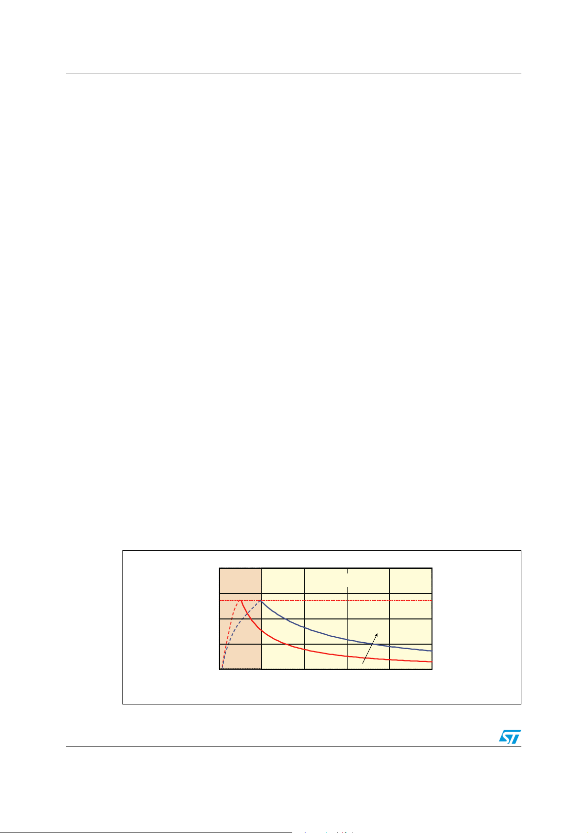
During this frequency sweep phase the operating frequency decays following the
exponential charge of C
: then, it initially changes relatively quickly but the rate of change
SS
gets slower and slower. This counteracts the non-linear frequency dependence of the tank
circuit that makes the converter's input impedance change little as frequency is away from
resonance and change very quickly as frequency approaches resonance frequency (see
Figure 13
).
Figure 12. Soft-start circuit Figure 13. Input impedance vs.
frequency curve in an LLC
resonant half bridge
500%22% 3/.!. #%
&2%15%. #9
3TEADY STATE
EQUENCY
FR
)NITIAL
FR
EQUENCY
!-V
F
2&M IN
,/7% 22%3/.!. #%
\:F\
2&M IN
2
33
#SS
#
33
,
!-V
&2%15%. #9
As a result, the DC input current smoothly increases, without the peaking that occurs with
linear frequency sweep, and the output voltage reaches the regulated value with almost no
overshoot.
Ty p ic al ly, R
and CSS is selected based on the following relationships:
SS
Equation 5
-
3
10 ·3
R
SS
SS
RF
min
=R
f
start
1
-
f
min
SS
=C;
where f
Figure 20
is recommended to not be over 300 kHz. Please refer to the timing diagram of
start
to see some significant signals during the soft-start phase.
20/38 Doc ID 022835 Rev 1

L6699 Operation at no load or very light load
!-V
,
34"9
2&M IN
2
&MI N
2
&MAX
,).%
2
!
"
2
"
2
,
2
(
2!2"2
,
7 Operation at no load or very light load
When the resonant half bridge is lightly loaded or totally unloaded, its switching frequency
reaches its maximum value. To keep the output voltage under control and avoid losing softswitching in these conditions, there must be some current flowing through the transformer's
magnetizing inductance. This current can be kept relatively low because of the adaptive
deadtime function; however, it produces power losses that prevent the converter's no load
consumption from achieving very low values anyhow.
To overcome this issue, the L6699 enables the user to make the converter operate
intermittently (burst-mode operation), with a series of a few switching cycles spaced out by
long idle periods where both MOSFETs are in the OFF-state, so that the average switching
frequency can be substantially reduced. As a result, the average value of the residual
magnetizing current and the associated losses is considerably cut down, therefore
facilitating the converter to comply with energy saving specifications.
The L6699 can be operated in burst-mode by using pin 5 (STBY): if the voltage applied to
this pin falls below 1.26 V, the IC enters an idle state where both gate-drive outputs are low,
the oscillator is stopped, the soft-start capacitor C
reference at the
RF
pin stays alive to minimize IC consumption and VCC capacitor
min
discharge. The IC resumes normal operation as the voltage on the pin exceeds 1.26 V by 30
mV.
keeps its charge and only the 2V
SS
In the L6699, the half bridge stops and restarts during burst-mode are more accurately
controlled with respect to its predecessors: the last cycle before stopping and the first cycle
after restarting are such that the DC voltage across the resonant capacitor Cr always stays
close to its steady-state value Vin/2. In this way, the anomalous current peaks due to V·s
unbalance in the transformer are minimized.
To implement burst-mode operation, the voltage applied to the STBY pin needs to be related
to the feedback loop.
Figure 14
shows the simplest implementation, suitable to a narrow
input voltage range (e.g. when there is a PFC front-end).
Figure 14. Narrow input voltage range Figure 15. Wide input voltage range
2&M IN
2
&MI N
2
&MAX
34"9
,
!-V
Essentially, RF
mode operation. Once f
defines the switching frequency f
max
max is
fixed, RF
is found from the relationship:
max
Doc ID 022835 Rev 1 21/38
above which the L6699 enters burst-
max

Operation at no load or very light load L6699
Equation 6
RF
max
3
=RF
8
min
·
f
max
1
-
f
min
Note that, unlike the f
some load Pout
greater than the minimum one. PoutB is normally such that the
B
considered in the
max
Section 6.1: Oscillator
, here f
is associated to
max
transformer's peak currents are low enough not to cause audible noise.
The resonant converter's switching frequency, however, depends also on the input voltage;
so, in case there is quite a large input voltage range, with the circuit of
Pout
would change considerably. In this case it is recommended to use the arrangement
B
shown in
Figure 15
, where the information on the converter's input voltage is added to the
Figure 14
the value of
voltage applied to the STBY pin. Due to the strongly non-linear relationship between
switching frequency and input voltage, it is more practical to find empirically the right amount
of correction R
the total value R
(see
Section 10: Line sensing function
/ (RA + RB) needed to minimize the change in PoutB. Take care in choosing
A
+ RB much greater than RL to minimize the effect on the LINE pin voltage
A
).
Figure 16. Load-dependent operating modes: timing diagram
34"9
HYSTER
6
F
,6'
(6'
0&#?34 /0
OSC
M6
T
T
T
0&#
'!4%
$2) 6%
2ESONANT-ODE "URST-ODE
Whichever circuit is in use, its operation can be described as follows. As the load falls below
the value Pout
voltage on the STBY pin (
the frequency tries to exceed the maximum programmed value f
B
V
) goes below 1.26 V. The IC then stops with both gate-drive
STBY
outputs low, so that both MOSFETs of the half bridge leg are in the OFF-state. The voltage
V
now increases as a result of the feedback reaction to the energy delivery stop and, as
STBY
it exceeds 1.29 V, the IC restarts switching. After a while,
response to the energy burst and stops the IC. In this way the converter works in a burstmode fashion with a nearly constant switching frequency. A further load decrease then
increases the time between consecutive bursts and/or reduces the duration of each burst.
This reduces the average switching frequency, which can go down even to few hundred
hertz. The timing diagram of
Figure 16
illustrates this kind of operation, showing the most
significant signals. A small capacitor (typically in the hundred pF) from the STBY pin to
ground, placed as close to the IC as possible to reduce switching noise pick-up, helps obtain
clean operation.
22/38 Doc ID 022835 Rev 1
2ESONANT-ODE
V
goes down again in
STBY
!-V
and the
max

L6699 Operation at no load or very light load
Figure 17. How the L6699 can switch off a PFC controller at light load
ZCD ( L6562)
Vcc
12
L6699
PFC_STOP
9
100 k
W
BC547
INV (L6562A)
22 k
W
BC547
L6562/2A
L6699
L6563S/H
L6564, L6564T/H
L4984
PFC_STOP9
PFC_OK
(AC_OK)
AM11388v1
To help the user meet energy saving requirements even in power-factor-corrected systems,
where a PFC pre-regulator precedes the DC-DC converter, the L6699 allows that the PFC
pre-regulator can be turned off during burst-mode operation, therefore eliminating the no
load consumption of this stage (0.5
- 1 W). There is no compliance issue in that, because
EMC regulations on low-frequency harmonic emissions refer to nominal load, no limit is
envisaged when the converter operates with light or no load.
To do so, the L6699 provides pin 8 (PFC_STOP): it is an open drain output, normally open,
that is asserted low when the IC is idle during burst-mode operation. This signal is externally
used for switching off the PFC controller and the pre-regulator as shown in
Figure 17
. When
the L6699 is in UVLO the pin is kept open to allow the PFC controller to start first.
The PFC_STOP pin is also used by some protection functions (OCP, OLP and latched
shutdown). Please refer to the relevant sections for more information.
Doc ID 022835 Rev 1 23/38

Current sensing, OCP and OLP L6699
!-V
,
)3% .
#R
#S
)
#R
2S
/PTIONAL
2
&
#
&
8 Current sensing, OCP and OLP
In the L6699 the current sense input ISEN (pin 6) senses the current flowing in the resonant
tank to perform multiple tasks:
1. Primary overcurrent protection (OCP function).
2. Hard-switching cycles prevention at startup (see
3. Capacitive-mode detection during operation (see
function
).
In this section the discussion is concentrated on the OCP function.
Unlike PWM-controlled converters, where energy flow is controlled by the duty cycle of the
primary switch (or switches), in a resonant half bridge the duty cycle is fixed and energy flow
is controlled by its switching frequency. This has an impact on the way current limitation can
be realized. While in PWM-controlled converters energy flow can be limited simply by
terminating switch conduction in advance when the sensed current exceeds a preset
threshold (cycle-by-cycle limitation), in a resonant half bridge the most efficient way to
reduce an excessive current level is to increase the switching frequency, i.e. the oscillator
frequency.
In
Figure 18
and 19 a couple of current sensing methods are illustrated.
Section 6.3: Safe-start procedure
).
Section 9: Capacitive-mode detection
Figure 18. Current sensing techniques
with sense resistor
)
#R
#R
2S
!-V
,
)3% .
/PTIONAL
2
#
&
&
Figure 19. Current sensing techniques
“lossless”, with capacitive
shunt
Note: The L6699 must sense the instantaneous tank current for proper operation of the smooth
startup function and the capacitive-mode detection circuit. Therefore, if a smoothing RC
circuit (the one shown in the dashed box) is used to reduce the noise level on the ISEN pin,
its time constant RF CF should be in the range of 100 - 200 ns. With slightly longer time
constants it is recommended that converter operation close to the capacitive-mode
boundary and during short-circuit, as well as at the end of the smooth-start phase, be
checked for possible hard-switching cycles. With considerably longer time constants (> 200
ns) hard-switching under the above mentioned conditions becomes very likely.
24/38 Doc ID 022835 Rev 1

L6699 Current sensing, OCP and OLP
The ISEN pin, which is also able to withstand negative voltages, is internally connected to
the input of a first comparator, referenced to
second comparator referenced to 1.5 V. The operation of the second comparator is
described later.
V
(0.8 V typ. 0.76 V min.), and to that of a
ISENx
If the voltage externally applied to the pin by either circuit in
the first comparator is tripped and this causes an internal switch to be turned on for 5 µs and
discharges the soft-start capacitor C
increases the oscillator frequency and thereby limits energy transfer. Under output shortcircuit conditions, this operation results in a peak primary current that periodically oscillates
below the maximum value allowed by the sense resistor Rs.
In the circuit shown in
value can be determined using the equation:
Equation 7
Figure 18
(see
SS
, Rs is placed directly in series to the resonant tank. Its
Section 6.3: Safe-start procedure
Figure 18
and 19 exceeds 0.8 V
). This quickly
76.0
=Rs
I
Crpkx
where I
and the primary winding of the transformer, which is related to the maximum load and the
minimum input voltage. The power dissipation in Rs can be approximately found with:
Equation 8
is the maximum expected peak current flowing through the resonant capacitor
Crpkx
I ·4.0P ≈
CrpkxRs
The circuit shown in
selected equal to Cr/100 or less and is a low-loss type, and the sense resistor Rs is selected
as:
Equation 9
and the associated power dissipation is reduced by a factor (1+Cr/Cs). This circuit is then
recommended when the efficiency target is very high.
This OCP is effective in limiting primary-to-secondary energy flow in case of an overload or
an output short-circuit, but the output current through the secondary winding and rectifiers
under these conditions may be so high that it endangers converter safety if continuously
flowing. To prevent any damage it is customary to force the converter to work intermittently,
which brings the average output current to values such that the thermal stress for the
transformer and the rectifiers can be easily handled.
If intermittent operation upon overload or short-circuit is desired, the designer can program
externally the maximum time T
conditions. Overloads or short-circuits lasting less than T
Figure 19
operates as a capacitive current divider; Cs is typically
77.0
=Rs
I
Crpkx
that the converter is allowed to run under these
SH
C
r
+1 ·
)(
Cs
do not cause any other action,
SH
Doc ID 022835 Rev 1 25/38

Current sensing, OCP and OLP L6699
therefore providing the system with immunity to short duration phenomena. If, instead, TSH
is exceeded, an overload protection (OLP) procedure is activated that shuts down the L6699
and, in case of continuous overload/short-circuit, results in continuous intermittent operation
with a user-defined duty cycle.
This function is realized on pin 2 (DELAY), with a capacitor C
R
connected to ground. As the voltage on the ISEN pin exceeds 0.8 V, the first OCP
Delay
comparator, in addition to turning on the switch that discharges C
generator that sources 350 µA for 50 µs from the DELAY pin and charges C
and a parallel resistor
Delay
, turns on a current
SS
Delay
. During an
overload/short-circuit the OCP comparator and the internal current source is repeatedly
activated and C
is charged with an average current depending essentially on CSS, RSS,
Delay
the characteristics of the resonant circuit, and the short-circuit impedance; the discharge
due to R
This operation continues until the voltage on C
the time T
not a simple relationship that links T
experimentally. As a rough indication, using 1 µF for C
is negligible because the associated time constant is typically much longer.
Delay
, V(DELAY), reaches 2 V, which defines
, or until the overload/short-circuit disappears, whichever occurs first. There is
SH
SH
to C
Delay
, so it is more practical to determine C
Delay
, TSH should be around 100 ms in
Delay
Delay
case of a dead short on the output.
In the case of an overload lasting less than T
decays with the time constant C
is shorter if this occurs before C
Delay·RDelay
is totally discharged. If, on the other hand, it is charged
Delay
up to 2 V, the internal switch that discharges C
SH
, C
is no longer charged, so its voltage
Delay
. Note that the value of TSH for the next overload
is continuously turned on, the PFC_STOP
SS
pin is pulled low, and the 350 µA current source is forced continuously on until V(DELAY)
reaches 3.5 V. This phase lasts:
Equation 10
C ·3.4T ≈
De layMP
with T
close to f
expressed in ms and C
MP
(see
start
Section 6.3: Safe-start procedure
in µF. During this time the L6699 runs at a frequency
Delay
resonant circuit. As V(DELAY) equals 3.5 V, the L6699 stops switching and the internal 350
µA generator is turned off, so that C
is slowly discharged by R
Delay
when V(DELAY) falls below 0.3 V, which takes:
Equation 11
33.0
The timing diagram of
voltage of the L6699 (V
does not restart immediately after V
Figure 20
CC
shows this operation. Note that if during TSTOP the supply
) falls below the UVLO threshold the IC records the event and
exceeds the startup threshold, if V(DELAY) is still
CC
higher than 0.3 V. Also the PFC_STOP pin stays low as long as V(DELAY) is greater than
0.3 V.
26/38 Doc ID 022835 Rev 1
) to minimize the energy inside the
. The IC restarts
Delay
5.3
≈
C ·R · 4.2ln ·C ·R=T
DelayDelayDelayDelaySTOP

L6699 Current sensing, OCP and OLP
Figure 20. Soft-start and delayed shutdown upon overcurrent timing diagram (safe-
start details are not shown)
).#!3%,)33%,&3500,)%$
4
-0
-).0/7%2
4
34/0
3(5 4$/ 7.
T
T
T
T
T
T
!-V
)3%.
$%,!9
6OUT
0&#?34 /0
6CC
#SS
6
34!2450
4
3(
4
6
6
6
6
6
SS
3/&4 34!2 4 3/&4 34!2 4
./2-!,
/0%2!4)/.
/6%2
,/!$
./2-!,
/0%2!4)/.
/6%2,/!$
In applications where continuous operation of the converter is needed even under overload
conditions, the delayed shutdown function can be disabled by simply grounding the DELAY
pin.
If the voltage on the ISEN pin reaches 1.5 V, the second comparator is triggered. Switching
is stopped immediately and both the internal switch that discharges C
and the 350 µA
SS
current source on the DELAY pin are forced continuously on. As V(DELAY) equals 3.5 V the
350 µA generator is turned off, so that C
is slowly discharged by R
Delay
. The L6699
Delay
restarts when V(DELAY) falls below 0.3 V.
Doc ID 022835 Rev 1 27/38

Capacitive-mode detection function L6699
9 Capacitive-mode detection function
Normally, the resonant half bridge converter operates with the resonant tank current lagging
behind the square-wave voltage applied by the half bridge leg, like a circuit having a
reactance of an inductive nature. In this way the applied voltage and the resonant current
have the same sign at every transition of the half bridge, which is a necessary condition in
order for soft-switching to occur (zero-voltage switching, ZVS at turn-on for both MOSFETs).
Therefore, should the phase relationship reverse, i.e. the resonant tank current anticipates
the applied voltage, like in circuits having a capacitive reactance, soft-switching would be
lost. This is termed capacitive-mode operation and must be avoided because of its
significant drawbacks:
1. Both MOSFETs feature hard-switching at turn-on, like in conventional PWM-controlled
converters (see
higher than the total power normally dissipated under “soft-switching” conditions and
this may easily lead to their overheating, since heatsinking is not usually sized to
handle this abnormal condition.
2. The body diode of the MOSFET just switched off conducts current during deadtime and
its voltage is abruptly reversed by the other MOSFET turned on (see
Therefore, once reverse-biased, the conducting body diode keeps its low impedance
until it recovers, therefore creating a condition equivalent to a shoot-through of the half
bridge leg. This is a potentially destructive condition (see next point) and causes
additional power dissipation due to the current and voltage of the conducting body
diode simultaneously high during part of its recovery.
3. There is an extremely high reverse dv/dt (many tens of V/ns!) experienced by the
conducting body diode at the end of its recovery with the other MOSFET turned on.
This dv/dt may exceed the rating of the MOSFET and lead to an immediate failure
because of the second breakdown of the parasitic BJT intrinsic in its structure. If a
MOSFET is hot, the turn-on threshold of its parasitic BJT is lower, and dv/dt-induced
failure is much more likely. The L6699 may be also damaged if its OUT pin is subject to
a dv/dt exceeding the AMR (50 V/ns).
Figure 21
). The associated capacitive losses may be considerably
Figure 21
).
Figure 21. Details of hard-switching transition during capacitive-mode operation
28/38 Doc ID 022835 Rev 1

L6699 Capacitive-mode detection function
4. When either MOSFET is turned on, the other one can be parasitically turned on too, if
the current injected through its Cgd and flowing through the gate driver's pull-down is
large enough to raise the gate voltage close to the turn-on threshold This would be a
lethal shoot-through condition for the half bridge leg.
5. The recovery of the body diodes generates large and energetic negative voltage spikes
because of the unavoidable parasitic inductance of the PCB subject to its di/dt. These
are coupled to the OUT pin and may damage the L6699.
6. There is a large common-mode EMI generation that adversely affects EMC.
Resonant converters work in capacitive mode when their switching frequency falls below a
critical value that depends on the loading conditions and the input-to-output voltage ratio.
They are especially prone to enter capacitive-mode when the input voltage is lower than the
minimum specified and/or the output is overloaded or short-circuited. Designing a converter
so that it never works in capacitive-mode, even under abnormal operating conditions, is
definitely possible but this may pose unacceptable design constraints in some cases.
To prevent the severe drawbacks of capacitive-mode operation, while enabling a design that
needs to ensure inductive-mode operation only in the specified operating range, neglecting
abnormal operating conditions, the L6699 provides the capacitive-mode detection function.
The IC monitors the phase relationship between the tank current circuit sensed on the ISEN
pin and the voltage applied to the tank circuit by the half bridge, checking that the former
lags behind the latter (inductive-mode operation). If the phase-shift approaches zero, which
is indicative of impending capacitive-mode operation, the monitoring circuit activates the
OCP procedure (see
Section 8: Current sensing, OCP and OLP
) so that the resulting
frequency rise keeps the converter away from that dangerous condition. Also in this case
the DELAY pin is activated, so that the OLP function, if used, is eventually tripped after a
time T
causing intermittent operation and reducing thermal stress.
SH
If the phase relationship reverses abruptly (which may happen in case of dead short at the
converter's output), the L6699 is stopped immediately, the soft-start capacitor C
discharged and a new soft-start cycle is initiated after 50
µs idle time. During this idle period
is totally
SS
the PFC_STOP pin is pulled low to stop the PFC stage as well.
Doc ID 022835 Rev 1 29/38

Line sensing function L6699
10 Line sensing function
This function basically stops the IC as the input voltage to the converter falls below the
specified range and lets it restart as the voltage goes back within the range. The sensed
voltage can be either the rectified and filtered mains voltage, in which case the function acts
as a brownout protection, or, in systems with a PFC pre-regulator front-end, the output
voltage of the PFC stage, in which case the function serves as a power-on and power-off
sequencing.
L6699 shutdown upon input undervoltage is accomplished by means of an internal
comparator, as shown in the block diagram of
available at pin 7 (LINE). The comparator is internally referenced to 1.22 V and disables the
IC if the voltage applied at the LINE pin is below the internal reference. Under these
conditions the soft-start is discharged, the PFC_STOP pin is open and the consumption of
the IC is reduced. PWM operation is re-enabled as the voltage on the pin is above the
reference. The comparator is provided with current hysteresis instead of a more usual
voltage hysteresis: an internal 13 µA current sink is ON as long as the voltage applied at the
LINE pin is below the reference and is OFF if the voltage is above the reference.
This approach provides an additional degree of freedom: it is possible to set the ON
threshold and the OFF threshold separately by properly choosing the resistors of the
external divider (see below). With voltage hysteresis, on the other hand, fixing one threshold
automatically fixes the other one depending on the built-in hysteresis of the comparator.
Figure 22
, whose non-inverting input is
With reference to
(Vin
) and OFF (Vin
ON
Equation 12
which, solved for R
Equation 13
Figure 22
ON
R
and RL, yields:
H
, the following relationships can be established for the ON
) thresholds of the input voltage:
OFF
25.1Vin -
-
H
=R
H
R
OFF
25.1Vin
25.1
=
R
LH
25.1
25.1Vin
-
25.1
-
6
+10 ·13=
R
VinVin
-
OFFON
6
10 · 13
;
L
OFF
R=R;
HL
30/38 Doc ID 022835 Rev 1

L6699 Line sensing function
Figure 22. Line sensing function: internal block diagram and timing diagram
(6)NP UTBUS
6IN
/.
6IN
/&&
,).%
(6 ) NP U TB U S
2
(
,).%
2
,
6CC
!
6
6
6IN/+
,
6
6IN / +
)
(93
!
6CC
,6'
(6'
6OU T
While the line undervoltage is active there is no switching activity, therefore the V
T
T
T
T
T
T
T
!-V
voltage
CC
(if not supplied by another source) continuously oscillates between the startup and the
UVLO thresholds, as shown in the timing diagram of
Figure 22
.
The LINE pin, while the device is operating, is a high impedance input connected to high
value resistors, so it is prone to pick-up noise,. This might alter Vin
or give rise to
OFF
undesired switch-off of the IC during ESD tests. It is possible to bypass the pin to ground
with a small film capacitor (e.g. 1-10 nF) to prevent any malfunctioning of this kind.
If the function is not used the pin can be pulled high by connecting it to V
resistor in the hundred k
Ω.
through a
CC
Doc ID 022835 Rev 1 31/38

Latched shutdown L6699
11 Latched shutdown
The L6699 is equipped with a comparator having the non-inverting input externally available
on pin 8 (DIS) and with the inverting input internally referenced to 1.85 V. As the voltage on
the pin exceeds the internal threshold, the IC is immediately shut down, the PFC_STOP pin
is asserted low and the quiescent consumption reduced to a low value. The information is
latched and it is necessary to let the voltage on the V
pin go below the UVLO threshold to
CC
reset the latch, de-assert the pin PFC_STOP, and restart the IC.
This function is useful to implement a latched overtemperature protection very easily by
biasing the pin with a divider from an external reference voltage (e.g. pin 4,
RF
), where
min
the upper resistor is an NTC physically located close to a heating element like the MOSFET,
or a secondary diode or the transformer.
An OVP can be implemented as well, e.g. by sensing the output voltage and transferring an
overvoltage condition via an optocoupler. A latch-mode OCP protection can be implemented
by connecting this pin to DELAY (pin 2).
12 Bootstrap section
The supply of the floating high-side section is obtained by means of a bootstrap circuitry.
This solution normally requires a high voltage fast-recovery diode (D
charge the bootstrap capacitor C
. In the L6699 a patented integrated structure,
BOOT
BOOT
,
Figure 23
) to
replaces this external diode. It is realized by means of a high voltage DMOS, working in the
third quadrant and driven synchronously with the low-side driver (LVG), with a diode in
series to the source, as shown in
The diode prevents that any current can flow from the
Figure 24
.
V
pin back to VCC if the supply is
BOOT
quickly turned off when the internal capacitor of the pump is not fully discharged. To drive
the synchronous DMOS, a voltage higher than the supply voltage V
voltage is obtained by means of an internal charge pump (
Figure 24
The bootstrap structure introduces a voltage drop while recharging C
is necessary. This
CC
).
(i.e. when the low
BOOT
side driver is on), which increases with the operating frequency and with the size of the
external Power MOSFET. It is the sum of the drop across the R
and the forward drop
DS(on)
across the series diode. At low frequency this drop is very small and can be neglected but,
as the operating frequency increases, it must be taken into account. In fact, the drop
reduces the amplitude of the driving signal and can significantly increase the R
DS(on)
of the
external high-side MOSFET and then its conductive loss.
32/38 Doc ID 022835 Rev 1

L6699 Bootstrap section
Figure 23. Bootstrap supply: standard
circuit
$
"//4
Figure 24. Bootstrap supply: internal
bootstrap synchronous diode
,6'
,
6"//4
/54
"//4
#
!-V
6CC
6"//4
/54
"//4
#
!-V
6CC
This concern applies to converters designed with a high resonance frequency (indicatively,
> 150 kHz), so that they run at high frequency also at full load. Otherwise, the converter runs
at high frequency at light load, where the current flowing in the MOSFETs of the half bridge
leg is low, so that, generally, a slight R
rise is not an issue. However, it is wise to check
DS(on)
this point anyway and the following equation is useful to estimate the drop on the bootstrap
driver:
Equation 14
Q
g
=V+RI=V
Fon)DS(eargchDrop
T
eargch
where Qg is the gate charge of the external Power MOSFET, R
the bootstrap DMOS (150
equals about half the switching period minus the deadtime T
Ω, typ.) and T
is the ON-time of the bootstrap driver, which
charge
D
V+R
Fon)DS(
is the ON-resistance of
DS(on)
. For example, using a
MOSFET with a total gate charge of 30 nC, the drop on the bootstrap driver is about 3 V at a
switching frequency of 200 kHz and with a deadtime of 300 ns:
Equation 15
9
-
Dro p
=V
10 · 30
66
-
--
10 · 3.010 ·5.2
V6.2=6.0+150
If a significant drop on the bootstrap driver is an issue, an external ultra-fast diode can be
used, therefore saving the drop on the R
of the internal DMOS. In this case it is also
DS(on)
recommended to add a small resistor (in the ten Ω) in series to the diode to prevent the
bootstrap capacitor from being charged to a voltage exceeding the absolute maximum rating
(18 V), in case of significant negative spikes on the half bridge midpoint when the high-side
MOSFET turns off.
Doc ID 022835 Rev 1 33/38

Package information L6699
13 Package information
In order to meet environmental requirements, ST offers these devices in different grades of
®
ECOPACK
specifications, grade definitions and product status are available at:
packages, depending on their level of environmental compliance. ECOPACK
www.st.com
. ECOPACK
is an ST trademark.
Figure 25. SO16N dimensions
mm
Dim.
Min. Typ. Max.
A 1.75
A1 0.10 0.25
A2 1.25
b0.31 0.51
c0.17 0.25
D 9.80 9.90 10.00
E5.806.006.20
E1 3.80 3.90 4.00
e1.27
h0.25 0.50
L0.40 1.27
k0 8°
ccc 0.10
34/38 Doc ID 022835 Rev 1

L6699 Package information
Figure 26. Package drawing
0016020_F
Doc ID 022835 Rev 1 35/38

Package information L6699
Figure 27. Recommended footprint (dimensions are in mm)
36/38 Doc ID 022835 Rev 1

L6699 Revision history
14 Revision history
Table 7. Document revision history
Date Revision Changes
12-Apr-2012 1 Initial release.
Doc ID 022835 Rev 1 37/38

L6699
Please Read Carefully:
Information in this document is provided solely in connection with ST products. STMicroelectronics NV and its subsidiaries (“ST”) reserve the
right to make changes, corrections, modifications or improvements, to this document, and the products and services described herein at any
time, without notice.
All ST products are sold pursuant to ST’s terms and conditions of sale.
Purchasers are solely responsible for the choice, selection and use of the ST products and services described herein, and ST assumes no
liability whatsoever relating to the choice, selection or use of the ST products and services described herein.
No license, express or implied, by estoppel or otherwise, to any intellectual property rights is granted under this document. If any part of this
document refers to any third party products or services it shall not be deemed a license grant by ST for the use of such third party products
or services, or any intellectual property contained therein or considered as a warranty covering the use in any manner whatsoever of such
third party products or services or any intellectual property contained therein.
UNLESS OTHERWISE SET FORTH IN ST’S TERMS AND CONDITIONS OF SALE ST DISCLAIMS ANY EXPRESS OR IMPLIED
WARRANTY WITH RESPECT TO THE USE AND/OR SALE OF ST PRODUCTS INCLUDING WITHOUT LIMITATION IMPLIED
WARRANTIES OF MERCHANTABILITY, FITNESS FOR A PARTICULAR PURPOSE (AND THEIR EQUIVALENTS UNDER THE LAWS
OF ANY JURISDICTION), OR INFRINGEMENT OF ANY PATENT, COPYRIGHT OR OTHER INTELLECTUAL PROPERTY RIGHT.
UNLESS EXPRESSLY APPROVED IN WRITING BY TWO AUTHORIZED ST REPRESENTATIVES, ST PRODUCTS ARE NOT
RECOMMENDED, AUTHORIZED OR WARRANTED FOR USE IN MILITARY, AIR CRAFT, SPACE, LIFE SAVING, OR LIFE SUSTAINING
APPLICATIONS, NOR IN PRODUCTS OR SYSTEMS WHERE FAILURE OR MALFUNCTION MAY RESULT IN PERSONAL INJURY,
DEATH, OR SEVERE PROPERTY OR ENVIRONMENTAL DAMAGE. ST PRODUCTS WHICH ARE NOT SPECIFIED AS "AUTOMOTIVE
GRADE" MAY ONLY BE USED IN AUTOMOTIVE APPLICATIONS AT USER’S OWN RISK.
Resale of ST products with provisions different from the statements and/or technical features set forth in this document shall immediately void
any warranty granted by ST for the ST product or service described herein and shall not create or extend in any manner whatsoever, any
liability of ST.
ST and the ST logo are trademarks or registered trademarks of ST in various countries.
Information in this document supersedes and replaces all information previously supplied.
The ST logo is a registered trademark of STMicroelectronics. All other names are the property of their respective owners.
© 2012 STMicroelectronics - All rights reserved
STMicroelectronics group of companies
Australia - Belgium - Brazil - Canada - China - Czech Republic - Finland - France - Germany - Hong Kong - India - Israel - Italy - Japan -
Malaysia - Malta - Morocco - Philippines - Singapore - Spain - Sweden - Switzerland - United Kingdom - United States of America
www.st.com
38/38 Doc ID 022835 Rev 1
 Loading...