

L6668
Fi
SMART PRIMARY CONTROLLER
1 General Features
■ MULTIPOWER BCD TECHNOLOGY
■ LOAD-DEPENDENT CURRENT-MODE CON-
TROL: FIXED-FREQUENCY (HEAVY LOAD),
FREQUENCY FOLDBACK (LIGHT LOAD),
BURST-MODE (NO-LOAD)
■ ON-BOARD HIGH-VOLTAGE START-UP
■ IMPROVED STANDBY FUNCTION
■ LOW QUIESCENT CURRENT (< 2 mA)
■ SLOPE COMPENSATION
■ PULSE-BY-PULSE & HICCUP-MODE OCP
■ INTERFACE WITH PFC CONTROLLER
■ DISABLE FUNCTION (ON/OFF CONTROL)
■ LATCHED DISABLE FOR OVP/OTP FUNC-
TION
■ PROGRAMMABLE SOFT-START
■ 2% PRECISION REFERENCE VOLTAGE EX-
TERNALLY AVAILABLE
■ ±800 mA TOTEM POLE GATE DRIVER WITH
INTERNAL CLAMP AND UVLO PULL-DOWN
■ BLUE ANGEL, ENERGY STAR, EU CODE OF
CONDUCT COMPLIANT
Figure 2. Block Diagram
S-COMP V
RCT
RCT
DIS
DIS
N.C.
N.C.
ISEN
ISEN
PFC_STOP
PFC_STOP
S-COMP V
SLOPE
SLOPE
COMP.
COMP.
16
16
TIMING
TIMING
+
+
7
7
-
-
2.2V
2.2V
6
6
HICCUP
HICCUP
12
12
+
+
-
-
1.5V
1.5V
14
14
DIS
DIS
OCP
OCP
CLK
CLK
-
-
+
+
2.2/2.7V
2.2/2.7V
HV
HV
1
1
BLANKING
BLANKING
R
R
SQ
SQ
and UVLO management
and UVLO management
R
R
SQ
SQ
+
+
PWM
PWM
-
OCP
OCP
0.8V 4R
0.8V 4R
9
9
SKIPADJ
SKIPADJ
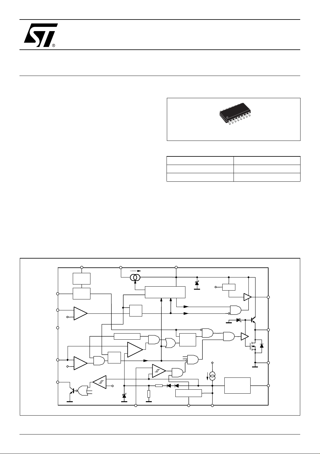
gure 1. Package
SO-16 (Narrow)
Table 1. Order Codes
Part Number Package
L6668 SO-16
L6668TR SO-16 in Tape & Reel
■ SO16 PACKAGE ECOPACK
®
1.1 APPLICATIONS
■ HI-END AC-DC ADAPTERS/CHARGERS FOR
NOTEBOOKS.
■ LCD/CRT MONITORS, LCD/CRT TV
■ DIGITAL CONSUMER
CC
CC
515
515
VREG
0.4mA
0.4mA
VREG
VREG
VREG
COMPSS
COMPSS
Vref
Vref
STANDBY
STANDBY
15V
15V
HV generator ON/OFF
HV generator ON/OFF
Vcc_OK
Vcc_OK
HYST. CTRL
HYST. CTRL
-
-
+
+
11R
11R
25V
25V
Vcc_OK
Vcc_OK
DIS
DIS
SQ
SQ
R
R
DIS
DIS
SOFT-START
SOFT-START
11 10
11 10
8
8
VREF
VREF
4
4
OUT
OUT
3
3
GND
GND
13
13
ST-BY
ST-BY
January 2006
Rev. 4
1/23
L6668
2 Description
L6668 is a current-mode primary controller IC, designed to build single-ended converters.
The IC drives the system at fixed frequency at heavy load and an improved Standby function causes a
smooth frequency reduction as the load is progressively reduced. At very light load the device enters a
special operating mode (burst-mode with fixed, externally programmed peak current) that, in addition to
the on-board high-voltage start-up and the very low quiescent current, helps keep low the consumption
from the mains and be compliant with energy saving regulations. To allow meeting compliance with these
standards in power-factor-corrected systems too, an interface with the PFC controller is provided that enables to turn off the pre-regulator when the load level falls below a threshold.
The IC includes also a programmable soft-start, slope compensation for stable operation at duty cycles
greater then 50%, a disable function, a leading edge blanking on current sense to improve noise immunity,
latched disable for OVP or OTP shutdown and an effective two-level OCP able to protect the system even
in case the secondary diode fails short.
Table 2. Absolute Maximum Ratings
Symbol Pin Parameter Value Unit
V
cc
V
HV
I
HV
--- Analog Inputs & Outputs, except pin 14 -0.3 to 8 V
I
PFC_STOP
V
PFC_STOP
P
tot
T
j
T
stg
Note: 1. ESD immunity for pin 1 is guaranteed up to 900V (Human Body Model).
5 IC Supply voltage (Icc = 20 mA) Self-limited V
1 High-voltage start-up generator voltage range -0.3 to 700 V
1 High-voltage start-up generator current Self-limited A
14 Max. sink current (low state) 2 mA
14 Max. voltage (open state) 16 V
Power Dissipation @Tamb = 50°C 0.75 W
Junction Temperature Operating range -25 to 150 °C
Storage Temperature -55 to 150 °C
1
Table 3. Thermal Data
Symbol Parameter Value Unit
R
th j-amb
Thermal Resistance Junction to AmbientMax 120 °C/W
Figure 3. Pin Connection (Top view)
2/23
HV
HV
HVS
HVS
GND
GND
OUT
OUT
Vcc
Vcc
N.C.
N.C.
DIS
DIS
VREF
VREF
RCT
RCT
S-COMP
S-COMP
PFC_STOP
PFC_STOP
STBY
STBY
ISEN
ISEN
SS
SS
COMP
COMP
SKIPADJ
SKIPADJ

Table 4. Pin Description
L6668
Pin
Number
1 HV High-voltage start-up. The pin is to be connected directly to the rectified mains voltage. A
2 HVS High-voltage spacer. The pin is not connected internally to isolate the high-voltage pin and
3 GND Chip ground. Current return for both the gate-drive current and the bias current of the IC. All
4 OUT Gate-drive output. The driver is capable of 0.8A min. source/sink peak current to drive
5 Vcc Supply Voltage of both the signal part of the IC and the gate driver. The internal high volt-
6 N.C. Connect the pin to GND.
7 DIS Latched device shutdown. Internally the pin connects a comparator that, when the voltage
8 VREF Voltage reference. An internal generator furnishes an accurate voltage reference (5V±4%,
9 SKIPADJ Burst-mode control threshold. A voltage is applied to this pin, derived from the reference
10 COMP Control input for PWM regulation. The pin is to be driven by the phototransistor (emitter-
11 SS Soft start. An internal 20µA generator charges an external capacitor connected between
12 ISEN Current sense (PWM comparator) input. The voltage on this pin is internally compared with
Pin Name Function
0.8 mA internal current source charges the capacitor connected between pin Vcc and GND
to start up the IC. When the voltage on the Vcc pin reaches the start-up threshold the generator is shut down. Normally it is re-enabled when the voltage on the Vcc pin falls below
5V, except under latched shutdown conditions, when it is re-enabled as the Vcc voltage falls
0.5V below the start-up threshold.
comply with safety regulations (creepage distance) on the PCB.
of the ground connections of the bias components should be tied to a track going to this pin
and kept separate from any pulsed current return.
MOSFET’s. The voltage delivered to the gate is clamped at about 15V so as to prevent too
high values when the IC is supplied with a voltage close to or exceeding 20V.
age generator charges an electrolytic capacitor connected between this pin and GND as
long as the voltage on the pin is below the start-up threshold of the IC, after that it is disabled. Sometimes a small bypass capacitor (0.1µF typ.) to GND might be useful to get a
clean bias voltage for the signal part of the IC.
on the pin exceeds 2.2V, shuts the IC down and brings its consumption to a value barely
higher than before start-up. The information is latched and it is necessary to recycle the
input power to restart the IC: the latch is removed as the voltage on the Vcc pin goes below
the UVLO threshold. Connect the pin to GND if the function is not used.
all inclusive) that can be used to supply up to 5 mA to an external circuit. A small film
capacitor (0.1µF typ.), connected between this pin and GND is recommended to ensure the
stability of the generator and to prevent noise from affecting the reference.
voltage VREF via a resistor divider. When the control voltage at pin COMP falls 50 mV
below the voltage on this pin the IC is shutdown and the consumption is reduced. The chip
is re-enabled as the voltage on pin COMP exceeds the voltage on the pin. The high-voltage
start-up generator is not invoked. The function is disabled during the soft-start ramp. The
pin must always be biased between 0.8 and 2.5V. A voltage between 0.8 and 1.4V disables
the function, if the pin is pulled below 0.8V the IC is shut down.
grounded) of an optocoupler to modulate the voltage by modulating the current sunk from
(sourced by) the pin (0.4 mA typ.). It is recommended to place a small filter capacitor
between the pin and GND, as close to the IC as possible to reduce switching noise pick up,
to set a pole in the output-to-control transfer function. A voltage 50 mV lower than that on
pin SKIPADJ shuts down the IC and reduces its current consumption.
the pin and GND generating a voltage ramp across it. This ramp clamps the voltage at pin
COMP during start-up, thus the duty cycle of the power switch starts from zero. During the
ramp all functions monitoring the voltage at pin COMP are disabled. The SS capacitor is
quickly discharged as the chip goes into UVLO.
an internal reference derived from the voltage on pin COMP and when they are equal the
gate drive output (previously asserted high by the clock signal generated by the oscillator)
is driven low to turn off the power MOSFET. The pin is equipped with 200 ns. min. blanking
time for improved noise immunity. A second comparison level located at 1.5V shuts the
device down and brings its consumption almost to a “before start-up” level.
3/23
L6668
Table 4. Pin Description (continued)
Pin
Number
Pin Name Function
13 STBY Standby function. This pin is a high-impedance one as long as the voltage on pin COMP is
higher than 3V. When the voltage on pin COMP falls below 3V, the voltage on the pin tracks
that on pin COMP and is capable of sinking current. A resistor connected from the pin to the
oscillator allows programming frequency foldback at light load.
14 PFC_STOP Open-drain ON/OFF control of PFC controller. This pin is intended for driving the base of a
PNP transistor in systems comprising a PFC pre-regulator, to stop the PFC controller at
light load by cutting its supply. The pin, normally low, opens if the voltage on COMP is lower
than 2.2V and goes back low when the voltage on pin COMP exceeds 2.7V. Whenever the
IC is shutdown, either latched (DIS >2.2V, ISEN >1.5V) or not (UVLO, SKIPADJ<0.8), the
pin is open as well.
15 S-COMP Voltage ramp for slope compensation. When the gate-drive output is high the pin delivers a
voltage tracking the oscillator ramp (shifted down by one V
); when the gate-drive output
BE
is low the voltage delivered is zero. The pin is to be connected to pin ISEN via a resistor to
make slope compensation and allow stable operation at duty cycles close to and greater
than 50%.
16 RCT Oscillator pin. A resistor to VREF and a capacitor to GND define the oscillator frequency (at
full load). A resistor connect to STBY modifies the oscillator frequency when the voltage on
pin COMP is lower than 3V.
Table 5. Electrical Characteristcs
(T
= 0 to 105°C, Vcc=15V, Co=1nF; RT =13.3k , CT =1nF; unless otherwise specified)
j
Symbol Parameter Test Condition Min. Typ. Max. Unit
SUPPLY VOLTAGE
Vcc Operating range After turn-on 9.4 22 V
V
CCOn
V
CCOff
Turn-on threshold
Turn-off threshold
Hys Hysteresis 4.0 V
V
Zener Voltage Icc = 20 mA 22 24 28 V
Z
SUPPLY CURRENT
I
start-up
I
I
CC
I
qdis
Start-up Current Before turn-on,
Quiescent Current After turn-on 2 2.5 mA
q
Operating Supply Current 4 mA
Shutdown quiescent
current
HIGH-VOLTAGE START-UP GENERATOR
V
V
HVstart
I
charge
I
HV, ON
I
HV, OFF
V
CCrestart
Breakdown voltage I
HV
Start voltage I
Vcc charge current VHV > V
ON-state current VHV > V
Leakage current (OFF state) VHV = 400 V 40 µA
HV generator restart voltage 4.4 5 5.6 V
(1)
(1)
After turn-on
12.5 13.5 14.5 V
8.0 8.7 9.4 V
150 µA
Vcc=Vcc
V
DIS
V
SKIPADJ
0.8 <V
< 100 µA 700 V
HV
< 100 µA 60 80 105 V
Vcc
V
HV
(1)
After DIS tripping
-0.5
ON
> 2.2, or V
> 1.5 180 µA
ISEN
<0.8 1 1.8 mA
> V
< V
COMP
Hvstart
Hvstart
Hvstart
SKIPADJ
, Vcc > 3V 0.55 0.85 1 mA
, Vcc > 3V 1.6 mA
, Vcc = 0 0.8
1.3 mA
12 13 14 V
4/23
Table 5. Electrical Characteristcs (continued)
(T
= 0 to 105°C, Vcc=15V, Co=1nF; RT =13.3k , CT =1nF; unless otherwise specified)
j
Symbol Parameter Test Condition Min. Typ. Max. Unit
REFERENCE VOLTAGE
V
V
REF
REF
I
REF
Output voltage
Total variation Vcc= 9.4 to 22 V,
Short circuit current V
Sink capability in UVLO Vcc = 6V; Isink = 0.5 mA 0.2 0.5 V
PWM CONTROL
V
COMP
I
COMP
R
D
D
COMP
max
min
Maximum level I
H
Max. source current V
Dynamic resistance V
Maximum duty cycle V
Minimum duty cycle V
CURRENT SENSE COMPARATOR
I
ISEN
t
LEB
t
d(H-L)
Input Bias Current V
Leading Edge Blanking After gate drive low-to-high
Delay to Output 100 ns
Gain 3.56 3.75 3.94 V/V
V
ISENx
V
ISENdis
Maximum signal V
Hiccup-mode OCP level
STANDBY FUNCTION
V
drop
V
th
V
- V
COMP
STBY
Threshold on V
COMP
Hysteresis 50 mV
LATCHED DISABLE FUNCTION
I
DIS
Input Bias Current V
Vth Disable threshold
OSCILLATOR
fsw Oscillation Frequency Tj = 25°C, V
Vpk Oscillator peak voltage
Vvy Oscillator valley voltage
SLOPE COMPENSATION
S-COMP
S-COMP
Ramp peak R
pk
Ramp starting value R
vy
Ramp voltage OUT pin low 0
Source capability V
SOFT-START
I
SSC
Charge current Tj = 25 °C 14 20 26 µA
(2)
Tj = 25 °C; I
REF
= 1 mA
4.925 5 5.075 V
4.8 5.13 V
I
= 1 to 5 mA
REF
= 0 10 30 mA
REF
=0 5.5 V
COMP
= 1 V 320 400 480 µA
COMP
= 2 to 4 V 22 kΩ
COMP
= 5 V 70 75 %
COMP
= 1 V 0 %
COMP
= 0 -1 µA
ISEN
160 225 290 ns
transition
= 5 V 0.725 0.8 0.875 V
COMP
(2)
I
= 0.8 mA, V
STBY
(2)
Voltage falling
= 0 to Vth -1 µA
DIS
(2)
voltage rising
COMP
Vcc = 9.4 to 22V, V
(2)
(2)
= 3 kΩ to GND,
S-COMP
OUT pin high, V
= 3 kΩ to GND,
S-COMP
<3V 35 mV
COMP
= 5 V 95 100 105 kHz
= 5 V 93 100 107 kHz
COMP
= 5V
COMP
1.35 1.5 1.65 V
3V
2.1 2.2 2.3 V
2.85 3 3.15 V
0.8 0.95 1.1 V
1.6 1.75 1.9 V
0.15 0.35 0.55 V
OUT pin high
S-COMP = VS-COMPpk
0.8 mA
L6668
5/23
L6668
Table 5. Electrical Characteristcs (continued)
(T
= 0 to 105°C, Vcc=15V, Co=1nF; RT =13.3k , CT =1nF; unless otherwise specified)
j
Symbol Parameter Test Condition Min. Typ. Max. Unit
V
SSsat
V
SSclamp
SKIPADJ FUNCTION
I
bias
V
SKIP
Hys Hysteresis Below V
V
OFF
PFC_STOP FUNCTION
I
leak
V
Vth Threshold for high level
Vth Threshold for high level
GATE DRIVER
V
V
OH
I
sourcepk
I
sinkpk
t
t
V
Oclamp
(1), (2)
Parameters in tracking each other
Low saturation voltage Duty cycle = 0 0.6 V
High saturation voltage 7 V
Input Bias Current V
= 0 to 4.5 V -1 µA
SKIP
Operating range 1.4 2.5 V
SKIP
25 85 mV
Shutdown threshold Voltage falling 0.8 V
High level leakage current V
Low saturation level I
L
Output Low Voltage I
OL
Output High voltage I
PFC_STOP
PFC_STOP
V
COMP
V
COMP
= 200 mA 1.0 V
sink
source
= 1mA, V
falling
rising
< 16V, V
(2)
(2)
= 2V 1 µA
COMP
= 4V 0.1 V
COMP
2.1 2.2 2.3 V
2.55 2.7 2.85 V
= 5 mA, Vcc = 12V 9.8 10.3 V
Peak source current -0.8 A
Peak sink current 0.8 A
Current Fall Time 30 ns
f
Current Rise Time 55 ns
r
Output clamp voltage I
UVLO saturation Vcc= 0 to Vccon, I
= 5mA; Vcc = 20V 10 12 15 V
source
= 2mA 1.1 V
sink
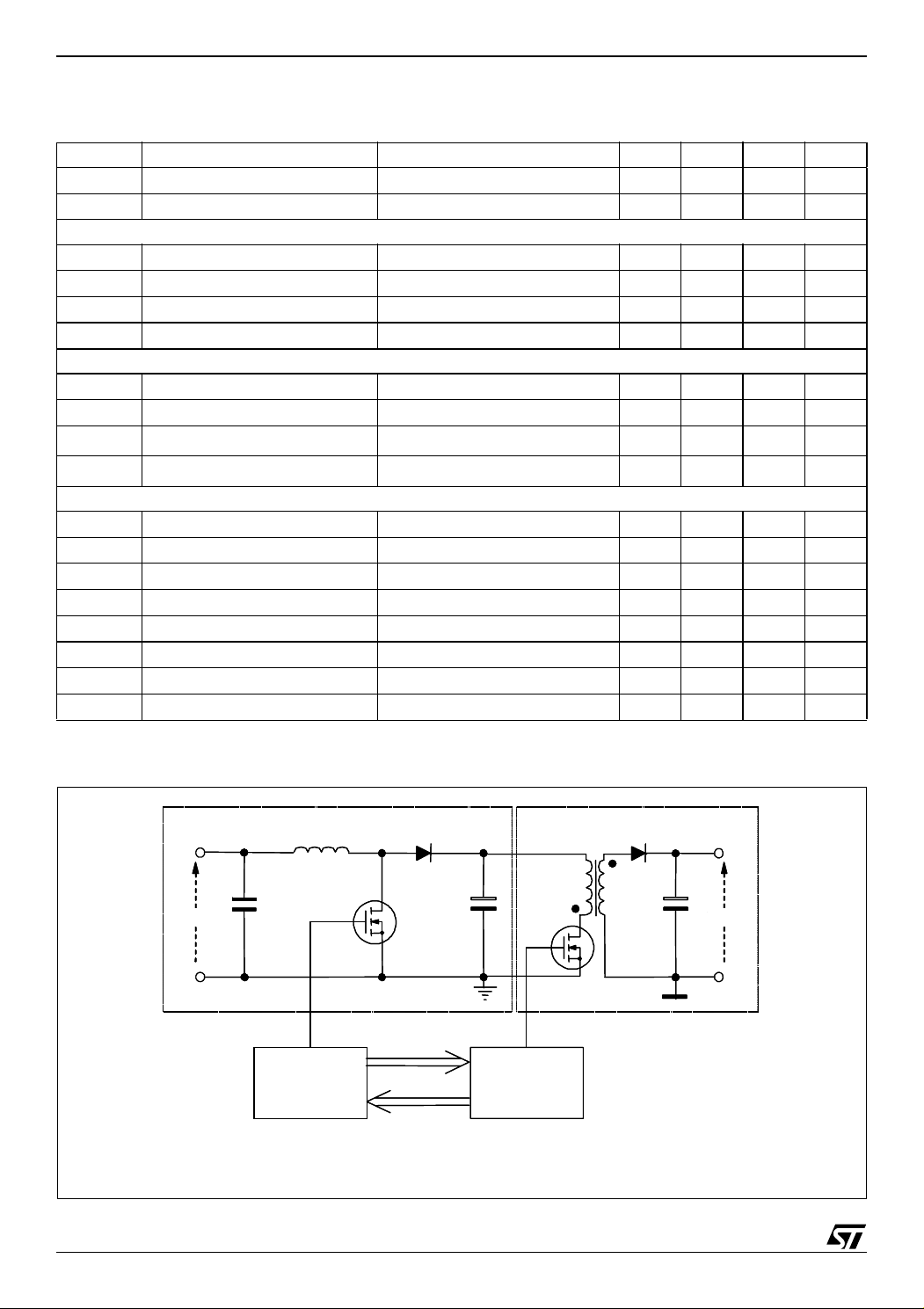
Figure 4. Typical System Block Diagram
PFC PRE-REGULATOR DC-DC CONVERTER
PFC PRE-REGULATOR DC-DC CONVERTER
V
V
inac
inac
PWM is turned off in case of PFC's
PWM is turned off in case of PFC's
anomalous operation, for safety
anomalous operation, for safety
L6561/2
L6561/2
or
or
L6563
L6563
PFC can be turned off at light
PFC can be turned off at light
load to ease compliance with
load to ease compliance with
energy saving regulations.
energy saving regulations.
6/23
L6668
L6668
V
V
outdc
outdc
3 Typical Electrical Performance
L6668
Figure 5. High-voltage generator ON-state sink current vs. Tj
HV
I
(pin 1)
1.2
[mA]
1
0.8
VHV = 100 V
0.6
0.4
0.2
-50 0 50 100 150
Vcc≥3V
Vcc = 0
Tj (°C)
Figure 6. High-voltage generator output (Vcc charge current) vs. Tj
Icc (pin 5)
120%
VHV = 100 V
110%
Figure 8. High-voltage generator start voltage vs. Tj
HV
120%
110%
100%
90%
Values normalized to VHV@ 25°C
80%
-50 0 50 100 150
Tj (°C)
Figure 9. High-voltage generator Vcc restart voltage vs. Tj
Vcc (pin 5)
14
[V]
12
while
latched off
100%
90%
Values normalized to Icc @ 25°C
80%
-50 0 50 100 150
Tj (°C)
Figure 7. High-voltage pin leakage vs. Tj
HV
I
(pin 1)
40
[µA]
VHV = 400 V
30
20
10
Vcc = 15V
0
-50 0 50 100 150
Tj (°C)
10
VHV = 100 V
8
6
4
-50 0 50 100 150
normal
operation
Tj (°C)
Figure 10. IC consumption vs. Tj
Icc (pin 5)
5
[mA]
3
2
1
Vcc = 15 V
Co = 1 nF
0.5
0.3
0.2
0.1
f = 100 kHz
Latched off
Before start-up (Vcc=12V)
-50 0 50 100 150
during burst-mode
Tj (°C)
Operating
Quiescent
Disa bled or
7/23

L6668
Figure 11. Start-up & UVLO vs. Tj
V
CC (pin 5)
(V)
14
ON
13
12
OFF while
latched off
11
10
9
8
OFF
-50 0 50 100 150
Tj (°C)
Figure 12. Vcc Zener voltage vs. Tj
Vcc
Z (pin 5)
(V)
26
25
24
23
22
21
Figure 14. COMP source current vs. Tj
(pin 10)
I
COMP
140%
120%
100%
80%
Values normalized to I
60%
-50 0 50 100 150
Tj (°C)
Vcc = 15 V
V
COMP
COMP
= 1 V
@ 25°C
Figure 15. COMP dynamic resistance vs. Tj
R
R
COMP (pin 1 0)
COMP (pin 1 0)
32
32
(kΩ)
(kΩ)
30
30
28
28
26
26
24
24
22
22
20
20
Vcc = 15 V
Vcc = 15 V
20
-50 0 50 100 150
Tj (°C)
Figure 13. COMP voltage upper clamp level vs. Tj
V
(pin 10)
COMP
7
8/23
(V)
6.5
6
5.5
5
-50 0 50 100 150
Tj (°C)
Vcc = 15 V
18
18
-50 0 50 100 150
-50 0 50 100 150
Tj (°C)
Tj (°C)
Figure 16. Max. duty-cycle vs. Tj
(%)
75
74
73
72
71
70
-50 0 50 100 150
Tj (°C)
Vcc = 15 V

L6668
Figure 17. Oscillator frequency vs. Tj
fsw
102%
101.5%
101%
100.5%
RT= 13.3 k
C
T = 1 nF
Ω
Vcc = 22V
Vcc = 15V
Vcc = 9.4V
100%
99.5%
Values normalized to fsw @ Tj=25°C, Vcc=15V
99%
-50 0 50 100 150
Tj (°C)
Figure 18. Oscillator ramp vs. Tj
Vpin14
3.5
(V)
3.0
2.5
Peak
Vcc = 15 V
Figure 20. Disable level on current sense vs. Tj
Vpin12
(V)
2.0
Vcc = 15 V
1.8
1.6
1.4
1.2
1.0
-50 0 50 100 150
Tj (°C)
Figure 21. Reference voltage vs. Tj
V
REF
(pin 8 )
(V)
5.1
Vcc = 15 V
5.05
2.0
1.5
Valley
1.0
0.5
-50 0 50 100 150
Tj (°C)
Figure 19. Current sense clamp vs. Tj
V
ISENx ( pin 12)
(V)
1
Vcc = 15 V
V
= Upper clamp
0.9
0.8
0.7
0.6
-50 0 50 100 150
COMP
Tj (°C)
5
4.95
4.9
-50 0 50 100 150
Tj (°C)
Figure 22. PFC_STOP open/low thresholds on
V
vs. Tj
COMP
V
COMP
(pin 10)
2.8
(V)
PFC_STOP low (voltage rising)
2.7
2.6
2.5
2.4
2.3
PFC_STOP open (voltage falling)
2.2
2.1
-50 0 50 100 150
Tj (°C)
Vcc = 15 V
9/23

L6668
Figure 23. Standby thresholds vs. Tj
V
COMP
(pin 10)
3.6
(V)
3.4
3.2
2.8
2.6
2.4
Disa ble (vo ltage risi ng)
3
Enable (voltage falling)
-50 0 50 100 150
Tj (°C)
Vcc = 15 V
Figure 24. Standby pin dropout vs. Tj
Vpin13 - Vpin10
0
(mV)
-5
-10
-15
-20
-25
Vcc = 15 V
V
= 2V
COMP
I
STBY = 0.8 mA
Figure 26. SKIPADJ hysteresis vs. Tj
Vpin9
100.0
(mV)
80.0
Vcc = 15 V
60.0
Vskipadj = 2.5 V
40.0
20.0
0.0
-50 0 50 100 150
Vskipadj = 1.4 V
Tj (°C)
Figure 27. SKIPADJ disable threshold vs. Tj
Vpin9
1.0
(V)
0.9
0.8
0.7
0.6
Vcc = 15 V
-30
-50 0 50 100 150
Tj (°C)
Figure 25. DIS threshold vs. Tj
V pin 7
2.5
(V)
2.4
2.3
2.2
2.1
2.0
-50 0 50 100 150
Tj (°C)
Vcc = 15 V
0.5
-50 0 50 100 150
Tj (°C)
Figure 28. Soft-start charge current vs. Tj
( pin11)
Iss
40.0
(µA)
30.0
20.0
10.0
Vcc = 15 V
0.0
-50 0 50 100 150
Tj (°C)
10/23

L6668
Figure 29. S-COMP ramp vs. Tj
Vpin15
2.0
(V)
Peak
1.5
Vcc = 15 V
R
S-SCOMP = 3 k
1.0
0.5
Valley
0.0
-50 0 50 100 150
Tj (°C)
Figure 30. UVLO saturation vs. Tj
Vpin4
1
(V)
0.9
0.8
Vcc = 0 V
Figure 32. Gate-drive output low saturation
V
pin4
[V]
5
4
Ω
3
2
1
0
0 200 400 600 800 1,000 1,200
Tj = 25 °C
Vcc = 12 V
SINK
IGD[mA]
Figure 33. Gate-drive output high saturation
V
pin4
[V]
Vcc - 2.0
Vcc - 3.0
Vcc - 4.0
Tj = 25 °C
Vcc = 12 V
SOURCE
0.7
0.6
0.5
-50 0 50 100 150
Tj (°C)
Figure 31. Gate-drive clamp vs. Tj
clamp
Vpin4
13
(V)
Vcc = 20 V
12.8
12.6
12.4
12.2
12
-50 0 50 100 150
Tj (°C)
Vcc - 5.0
Vcc - 6.0
0 200 400 600 800 1,000
IGD[mA]
11/23

L6668
4 Application Information
The L6668 is a versatile current-mode PWM controller specific for offline fixed-frequency, peak-currentmode-controlled flyback converters.
The device is able to operate in different modes (fig. 34), depending on the converter's load conditions:
1) Fixed frequency at heavy load. In this region the IC operates exactly like a standard current mode control
chip: a relaxation oscillator, externally programmable with a capacitor and a resistor, generates a sawtooth
and releases a clock pulse during the falling edge of the sawtooth; the power switch is turned on by the clock
pulses and is turned off by the control loop.
2) Frequency-foldback mode at medium and light load. As the load is reduced the oscillator frequency is reduced as well by slowing down the charge of the timing capacitor proportionally to the load itself.
3) Burst-mode control with no or very light load. When the load is extremely light or disconnected, the converter
will enter a controlled on/off operation with constant peak current. A load decrease will be then translated
into a frequency reduction, which can go down even to few hundred hertz, thus minimizing all frequencyrelated losses and making it easier to comply with energy saving regulations. Being the peak current very
low, no issue of audible noise arises.
Figure 34. Multi-mode operation of the L6668
Frequency foldback mode
Burs t mode
sw
f
0
0
in
P
Fixed-frequency mode
Pinmax
4.1 High-voltage start-up generator
Figure 35 shows the internal schematic of the high-voltage start-up generator (HV generator). It is made
up of a high-voltage N-channel FET, whose gate is biased by a 15 M
Ω resistor, with a temperature-com-
pensated current generator connected to its source.
Figure 35. High-voltage start-up generator: internal schematic
HV
3
GND
1
I
HV
Vcc
5
I
charge
L6668 15 M
Vcc_OK
Ω
HV_EN
CONTR OL
The HV generator is physically located on a separate chip, made with BCD off-line technology able to withstand 700V, controlled by a low-voltage chip, where all of the control functions reside.
12/23

L6668
With reference to the timing diagram of figure 36, when power is first applied to the converter the voltage
on the bulk capacitor (Vin) builds up and, as it reaches about 80V, the HV generator is enabled to operate (HV_EN is pulled high) so that it draws about 1 mA. This current, diminished by the IC consumption,
charges the bypass capacitor connected between pin Vcc (5) and ground and makes its voltage rise almost linearly.
Figure 36. Timing diagram: normal power-up and power-down sequences
Vin
Vin
V
V
HVstar t
HVstar t
regulation is lost here
Vcc
Vcc
Vcc
Vcc
Vcc
Vcc
Vcc
Vcc
ON
OFF
OFF
restart
restart
OUT
OUT
HV_EN
HV_EN
Vcc_OK
Vcc_OK
regulation is lost here
ON
t
t
t
t
t
t
t
t
I
1 mA
1 mA
I
HV
HV
Normal
Power-up Power-down
Power-up Power-down
Normal
operation
operation
t
t
t
t
As the Vcc voltage reaches the start-up threshold (13.5V typ.) the low-voltage chip starts operating and
the HV generator is cut off by the Vcc_OK signal asserted high. The IC is powered by the energy stored
in the Vcc capacitor until the self-supply circuit (typically an auxiliary winding of the transformer and a
steering diode) develops a voltage high enough to sustain the operation.
The residual consumption of this circuit is just the one on the 15M
Ω resistor (≈10 mW at 400 Vdc), typically
50-70 times lower, under the same conditions, as compared to a standard start-up circuit made with an
external dropping resistor.
Figure 37. Timing diagram showing short-circuit behavior
Short circuit occurs here
Short circuit occurs here
t
t
t
t
VccON
VccON
VccOFF
VccOFF
Vccrest
Vccrest
OUT
OUT
Vcc_OK
Vcc_OK
Vcc
Vcc
1 mA
1 mA
HV
HV
I
I
t
t
t
t
13/23

L6668
At converter power-down the system will lose regulation as soon as the input voltage is so low that either
peak current or maximum duty cycle limitation is tripped. Vcc will then drop and stop IC activity as it falls
below the UVLO threshold (8.7V typ.).
The Vcc_OK signal is de-asserted as the Vcc voltage goes below a threshold Vcc
5V. The HV generator can now restart but, if Vin < V
, as shown in figure 36, HV_EN is de-asserted
instart
too and the HV generator is disabled.
This prevents converter's re-start attempts and ensures monotonic output voltage decay at power-down.
The low restart threshold Vcc
ensures that, during short circuits, the restart attempts of the L6668 will
restart
have a very low repetition rate, as shown in the timing diagram of figure 37, and that the converter will
work safely with extremely low power throughput.
4.2 Frequency Foldback Block and operation at medium/light load
At heavy load, namely as the voltage on pin COMP (V
) is higher than 3V, the device works at a fixed
COMP
frequency like a standard current mode PWM controller.
As the load is reduced, and the V
voltage falls below 3V (approximately corresponding to 50% of the
COMP
maximum load in a fully DCM system), the oscillator frequency can be made dependent on converter's
load conditions - the lower the load, the lower the frequency and vice versa.
Figure 38. Frequency foldback function: oscillator frequency is a function of COMP voltage
located at about
restart
f
f
osc
STBY
STBY
T
T
osc
L6668
L6668
COMP
COMP
3.0V
3.0V
-
-
+
+
OSCILLATOR
OSCILLATOR
13
13
8
8
16
16
This is done by adding an external resistor R
STBY
STBY
Vref
Vref
R
R
R
R
T
T
RCT
RCT
C
C
between pins RCT (#16) and STBY (#13), which acti-
STBY
vates the circuit shown in figure 38.
When V
nected to a current sink, tracks V
is below 3 V (oscillator's peak voltage) the voltage on the STBY pin, which is internally con-
COMP
and then some of the current that charges CT is diverted to ground
COMP
through the STBY pin.
In this way the rate of rise of the voltage across C
the lower V
the lower the frequency. Instead, when V
COMP
high impedance and the oscillator frequency f
is slowed down and the oscillator frequency decreased,
T
will be determined by RT and CT. These components can
osc
is greater than 3 V the STBY pin features
COMP
be then calculated as it is usually done with this type of oscillator:
RTC
1.4
---------=
T
f
osc
R
R
STBY
STBY
1.4 3.0 4.4
1.4 3.0 4.4
V
V
COMP
COMP
14/23

Figure 39. Standby function: frequency shift vs. timing resistors (normalized quantities)
1
1
0.9
0.9
0.8
0.8
0.7
0.7
f
f
min
min
0.6
0.6
f
f
osc
osc
0.5
0.5
0.4
0.4
0.3
0.3
0.2
0.2
0. 1 10
0. 1 10
2.5V
2.5V
2.2V
2.2V
2V
2V
1.8V
1.8V
V(SKIPADJ) = 1.6V
V(SKIPADJ) = 1.6V
V(SKIPADJ) = 1.5V
V(SKIPADJ) = 1.5V
V(SKIPADJ) = 1.4V
V(SKIPADJ) = 1.4V
R
R
STBY
STBY
R
R
T
T
L6668
The determination of R
mode operation takes place (f
can be done assuming that the minimum switching frequency before burst-
STBY
) is specified. This value will be above the audible range to ensure a
min
noise-free operation. With the aid of the diagrams in figure 39, which show the relationship between the
frequency shift obtained and the ratio of R
possible to determine R
. Draw an horizontal line corresponding to the desired f
STBY
to RT for different values of the burst-mode threshold, it is
STBY
ratio as long as
min/fosc
it intercepts the characteristic corresponding to the voltage set at the pin SKIPADJ (#9). From there, draw
a vertical line: on the horizontal axis it is possible to read the required R
STBY/RT
ratio.
Note that the characteristic for V(SKIPADJ)=1.4V corresponds to the burst-mode operation not used (see
next section). Note also that, for a given V(SKIPADJ), there is both a lower limit to the R
STBY/RT
ratio and
a maximum frequency shift allowed. Not observing these limits will result in erratic behavior.
In applications where the switching frequency needs not be tightly fixed for some specific reason there is
no major drawback to this technique. In case this function is not desired, the STBY pin shall be left open.
4.3 Operation at no load or very light load
When the PWM control voltage at pin COMP falls about 50 mV below a threshold externally programmable via pin 9 (SKIPADJ), the IC is disabled with the MOSFET kept in OFF state and its consumption reduced at a very low value to minimize Vcc capacitor discharge. The soft-start capacitor is not discharged.
The control voltage now will increase as a result of the feedback reaction to the energy delivery stop, the
threshold will be exceeded and the IC will restart switching again. In this way the converter will work in
burst-mode with a constant peak current defined by the disable level applied at pin 9. A load decrease will
then cause a frequency reduction, which can go down even to few hundred hertz, thus minimizing all frequency-related losses and maximizing efficiency. This kind of operation is noise-free provided the peak
current, which is user-defined by the bias voltage at pin 9, is very low.
The timing diagram of figure 40 illustrates this kind of operation along with the other ones, showing the
most significant signals.
15/23

L6668
Figure 40. Load-dependent operating modes: timing diagram
COMP
3.0V
V(SKIPADJ)
50 mV
hyster.
f
osc
t
t
OUT
Fix. Fr eq.
Mode
Burst-mode
Frequency Foldback Mode
Fix. Fr eq.
t
Mode
The operating range of the voltage V(SKIPADJ) is practically limited upwards by the onset of audible
noise: typically, with a voltage above 2-2.1V some noise can be heard under some line/load conditions. If,
instead, V(SKIPADJ) is set below the low saturation value of the PWM control voltage (1.4V typ.) burstmode operation will never take place. Always bias the pin at some voltage, a floating pin will result in
anomalous behavior. The SKIPADJ pin doubles its function: if the voltage is pulled below 0.8V the IC is
disabled completely, except for the externally available reference voltage VREF, and its quiescent consumption reduced. The soft-start capacitor is discharged so that, when the voltage on the SKIPADJ pin is
pulled above 0.8V, the chip is soft-started just like exiting from UVLO. This function is useful for some kind
of remote ON/OFF control. The comparator referenced to 0.8V does not have hysteresis; hence make
sure that the voltage on the pin does not linger on the threshold to prevent uncertain behavior.
4.4 PWM control Block
The device is specific for secondary feedback. Typically, there is a TL431 at the secondary side and an
optocoupler that transfers output voltage information to the PWM control at the primary side, crossing the
isolation barrier. The PWM control input (pin #10, COMP) is driven directly by the phototransistor's collector (the emitter is grounded to GND) to modulate the duty cycle.
4.5 Current Comparator, PWM Latch and Hiccup-mode OCP
The current comparator senses the voltage across the current sense resistor (Rs) on pin 12 (ISEN) and,
by comparing it with the programming signal derived form the control voltage on pin 10 (COMP), determines the exact time when the external MOSFET is to be switched off. The PWM latch avoids spurious
switching of the MOSFET, which might result from the noise generated ("double-pulse suppression").
16/23

Figure 41. Hiccup-mode OCP: timing diagram
Secondary diode is shorte d here
Vcc
Vcc
Vcc
Vcc
Vcc
Vcc
OFF
OFF
V
V
OUT
OUT
OCP latch
OCP latch
Vcc_OK
Vcc_OK
ON
ON
re
re
1.5 V
CS
CS
1.5 V
Secondary diode is shorte d here
L6668
t
t
t
t
t
t
t
t
t
t
A second comparator senses the voltage on the current sense input and shuts the IC down if the voltage
at the pin exceeds 1.5 V. Such an anomalous condition is typically generated by either a short circuit of
the secondary rectifier or a shorted secondary winding or a saturated flyback transformer.
This condition is latched as long as the IC is supplied. When the IC is disabled, however, no energy is
coming from the self-supply circuit, then the voltage on the Vcc capacitor will decay and cross the UVLO
threshold after some time, which clears the latch. The internal start-up generator is still off, then the Vcc
voltage still needs to go below its restart voltage before the Vcc capacitor is charged again and the IC restarted.
Ultimately, either of the above mentioned failures will result in a low-frequency intermittent operation (Hiccup-mode operation), with very low stress on the power circuit. The timing diagram of figure 41 illustrates
this operation.
4.6 Power Management
The L6668 is specifically designed to minimize converter's losses under light or no-load conditions, and a
special function has been provided to help the designer meet energy saving requirements even in powerfactor-corrected systems where a PFC pre-regulator precedes the DC-DC converter.
Actually EMC regulations require compliance with low-frequency harmonic emission limits at nominal
load, no limit is envisaged when the converter operates with a light load. Then the PFC pre-regulator can
be turned off, thus saving the no-load consumption of this stage (0.5 to 1W).
To do so, the device provides the PFC_STOP (#14) pin: it is an open collector output, normally low, that
becomes open when the voltage V
falls below 2.2V.
COMP
This signal will be externally used for switching off the PFC controller and the pre-regulator as shown in
figure 42. To prevent intermittent operation of the PFC stage, 0.5V hysteresis is provided: the PFC_STOP
pin is re-asserted low (which will re-enable the PFC pre-regulator) when V
exceeds 2.7 V.
COMP
A capacitor (and a limiting resistor in the hundred ohms), shown in dotted lines, may be used if one wants
to delay PFC turn-off
When the L6668 is in UVLO (Vcc<8.7V) the pin is kept high so as to ensure that the PFC pre-regulator
will start up only after the DC-DC converter governed by the L6668 is activated.
17/23

L6668
Figure 43 shows a timing diagram where the PFC_STOP function operation is illustrated under different
operating conditions.
Figure 42. How the L6668 can switch off a PFC controller at light load
BC557
BC557
Vcc
Vcc
16
16
PFC_STOP14
L6668
L6668
PFC_STOP14
Figure 43. Operation of PFC_STOP function
Vcc
ON
Vcc
OFF
Vcc
10 k
10 k
2.2 k
2.2 k
Ω
Ω
8.2 V
8.2 V
Ω
Ω
Vcc
Vcc
PFC
PFC
controller
controller
PFC_STOP
COMP
2.2V
OUT
PFC
Gate
Drive
Star t-up Full -load Light- load Full- load
Figure 44. Operation after DIS pin activation: timing diagram
DIS
DIS
2.2V
2.2V
Vcc
Vcc
VccON
VccON
HV generator is tur ned on
VccON -0.5
VccON -0.5
VccOFF
VccOFF
Vccrest
Vccrest
OUT
OUT
HV generator is tur ned on
HV generator is disabled here
HV generator is disabled here
2.7V
Disabl e latch is rese t here
Disabl e latch is rese t here
t
t
t
t
t
t
t
t
t
18/23
V
V
Vin
Vin
HVstart
HVstart
Input source is removed here
Input source is removed here
t
t
t
t

L6668
4.7 Disable function
Latched OTP or OVP functions can be easily realized with the L6668: the IC is equipped with a comparator whose non-inverting input is externally available on pin #7 (DIS), and whose inverting input is internally referenced to 2.2V.
As the voltage on the pin exceeds the threshold the IC is immediately shut down and its consumption reduced at a low value. The information is latched and it is necessary to let the voltage on the Vcc pin go
below the UVLO threshold to reset the latch and restart the IC.
To keep the latch supplied as long as the converter is connected to the input source, the HV generator is
activated periodically so that Vcc oscillates between the start-up threshold V
then necessary to disconnect the converter from the input source to restart the IC. This operation is shown
in the timing diagram of figure 44. Activating the HV generator in this way cuts its power dissipation approximately by three and keeps peak silicon temperature close to the average value.
4.8 Slope compensation
A pin of the device (#15, S-COMP) provides a voltage ramp during MOSFET's ON-time which is a repetition of the oscillator sawtooth, buffered (0.8 mA min. capability) and level shifted down by one Vbe.
This ramp is intended for implementing additive slope compensation on current sense. This is needed to
avoid the sub-harmonic oscillation that arises in all peak-current-mode-controlled converters working in
continuous conduction mode with a duty cycle close to or exceeding 50%.
Figure 45. Slope compensation waveforms
ccON
and V
- 0.5V. It is
ccON
RCT
RCT
t
OUT
OUT
S-COMP
S-COMP
t
t
t
t
t
The compensation will be realized by connecting a programming resistor between this pin and the current
sense input (pin 12, ISEN). The pin has to be connected to the sense resistor with another resistor to make
a summing node on the pin.
Since no ramp is delivered during MOSFET OFF-time (see figure 45), no external component other than
the programming resistor is needed to ensure a clean operation at light loads. If slope compensation is
not required the pin shall be left floating.
19/23

L6668
Figure 46. Typical Application: 80W, WRM flyback; Electrical Schematic
T1: CORE E32/16/9, N67
T1: CORE E32/16/9, N67
PRIM. IND. 430µH; lgap = 1mm
PRIM. IND. 430µH; lgap = 1mm
R1
R1
3 MΩ
3 MΩ
R2
R2
3 MΩ
3 MΩ
R3 10Ω
R3 10Ω
R710Ω
R710Ω
R12 1kΩ
R12 1kΩ
D1
D1
1.5KE200
1.5KE200
D2
D2
STTH1L06
STTH1L06
D3 1N4148
D3 1N4148
R13A,B
R13A,B
0.56
0.56
1/2W
1/2W
N1
N1
56T
56T
N3
N3
8T
8T
Q1
Q1
STP9NK65
STP9NK65
T1
T1
C4
C4
100 nF
100 nF
F1 T2A250V
F1 T2A250V
J1
J1
88 to 264
88 to 264
Vac
Vac
4.03 kΩ
4.03 kΩ
R9
R9
6.2 kΩ
6.2 kΩ
3.3 nF
3.3 nF
C3 100 nF
C3 100 nF
R8
R8
C5
C5
STBY
STBY
RCT
RCT
NTC1
NTC1
VREF
VREF
16
16
13
13
N.C.
N.C.
82.5 kΩ
82.5 kΩ
BD1
BD1
DF04M
DF04M
C1
C1
100 µF
100 µF
400 V
400 V
R5 47kΩ
R5 47kΩ
S-COMP
S-COMP
815
815
L6668
L6668
6
R10
R10
6
9
9
47 kΩ
47 kΩ
56 nF
56 nF
R11
R11
R4
R4
330 k
330 k
Ω
Ω
C2
C2
25 V
25 V
47 µF
47 µF
R6
R6
9.1 kΩ
9.1 kΩ
VCC
VCC
DIS
DIS
11
11
SS
SS
C6
C6
HV
HV
OUT
OUT
57
57
4
4
1
1
ISEN
ISEN
12
12
10
10
3
3
COMPSKIPADJ
COMPSKIPADJ
GND
GND
OC1
OC1
PC817A
PC817A
C7
C7
2.2 nF
2.2 nF
D4
D4
STPS20150CT
STPS20150CT
N2
N2
10T
10T
C12
C12
2.2 nF
2.2 nF
Y1
Y1
R14
R14
4.3 kΩ
4.3 kΩ
OC1
OC1
PC817A
PC817A
TL431
TL431
1
1
2
2
3
3
C8A,B,C
C8A,B,C
680 µF
680 µF
25 V
25 V
1.2 kΩ
1.2 kΩ
R15
R15
C10
C10
100 nF
100 nF
R16
R16
47 kΩ
47 kΩ
R18
R18
1.3 kΩ
1.3 kΩ
C9
C9
100 nF
100 nF
8.06 kΩ
8.06 kΩ
R17
R17
18V/4.5A
18V/4.5A
GND
GND
J2
J2
Table 6. Light load measurements on the circuit of figure 46
Output power Test condition Input power
Pout = 0.5 W Vin= 110 Vac 0.71 W
Vin= 230 Vac 0.86 W
Pout = 0 W Vin= 110 Vac 0.09 W
Vin= 230 Vac 0.17 W
20/23

L6668
5 Package information
In order to meet environmental requirements, STMicroelectronics offers this device in ECOPACK® package. This package has a Lead-free second level interconnect. The category of second level Interconnect
is marked on the package and on the inner box label, in compliance with JEDEC Standard JESD97.
The maximum ratings related to soldering conditions are also marked on the inner box label. ECOPACK
is an STMicroelectronics trademark.
ECOPACK specifications are available at: www.st.com.
Figure 47. SO16 (Narrow) Mechanical Data & Package Dimensions
DIM.
A 1.75 0.069
a1 0.1 0.25 0.004 0.009
a2 1.6 0.063
b 0.35 0.46 0.014 0.018
b1 0.19 0.25 0.007 0.010
C 0.5 0 .020
c1 45° (typ.)
(1)
D
E 5.8 6.2 0.228 0.244
e 1.27 0.050
e3 8.89 0.350
(1)
F
G 4 .60 5.30 0.181 0.208
L 0.4 1.27 0.150 0.050
M 0.62 0.024
S8° (max.)
(1) "D" an d "F" do not i nclude mold f lash or protru sions - Mold
flash or protr usions shall not ex ceed 0.15mm (.006 inc.)
mm inch
MIN. TYP. MAX. MIN. TYP. MAX.
9.8 10 0.386 0.394
3.8 4.0 0.150 0.157
OUTLINE AND
MECHANICAL DATA
SO16 (Narrow)
0016020 D
21/23

L6668
6 Revision History
Table 7. Revision History
Date Revision Description of Changes
20-May-2005 1 First Issue.
15-July-2005 2 Modify values in Electrical Characteristics
28-July-2005 3 Changed the maturity from “Preliminary Data” to “Datasheet”.
13-Jan-2006 4 Absolute Maximum Rating Update (added ESD note for pin 1).
Modified value “DIS >2.2V” in the table 4 pin 14.
22/23

L6668
Information furnished is believed to be accurate and reliable. However, STMicroelectronics assumes no responsibility for the consequences
of use of such information nor for any infringement of patents or other rights of third parties which may result from its use. No license is granted
by implication or otherwise under any patent or patent rights of STMicroelectronics. Specifications mentioned in this publication are subject
to change without notice. This publication supersedes and replaces all information previously supplied. STMicroelectronics products are not
authorized for use as critical components in life support devices or systems without express written approval of STMicroelectronics.
The ST logo is a registered trademark of STMicroelectronics.
All other names are the property of their respective owners
© 2006 STMicroelectronics - All rights reserved
Australia - Belgium - Brazil - Canada - China - Czech Republic - Finland - France - Germany - Hong Kong - India - Israel - Italy - Japan -
Malaysia - Malta - Morocco - Singapore - Spain - Sweden - Switzerland - United Kingdom - United States of America
STMicroelectronics group of companies
www.st.com
23/23
 Loading...