

®
90V BCD MIXED TECHNOLOGY
SO24 PLASTIC SMD PACKAGE
4.5 TO 13.2V OPERATIVE VOLTAGE
±25 TO ±35V OUTPUT VOLTAGE RANGE
SELECTABLE BY EXTERNAL RES ISTO RS
FULL-WAVE RESONANT DC-DC CON-
VERTER USING SINGLE COIL FOR DUAL
HIGH VOLTAGE GENERATOR WITH OUTPUT SLEW RATE CONTROL AND SELF
CURRENT LIMITING FOR LOW EMI
±35V OR 0/+70V OPERATIVE VOLTAGE
DRIVING CONFIGURATION MODES:
1. SINGLE ENDED VOLTAGE MODE
2. DIFFERENTIAL VOLTAGE MODE
3. SINGLE ENDED CHARGE MODE
DOUBLE OPERATIONAL AM PLIFIERS WITH
500KHZ GAIN BANDWIDTH PRODUCT AND
LOAD DRIVING CAPABILITY FROM 0.4nF
UP TO 24nF
ANALOG VOLTAGE SHIFTING CIRCUITRY
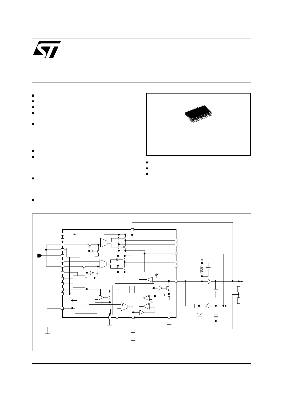
L6660
MILLI-ACTU A TO R DR IVER
PRODUCT PREVIEW
SO24(Shrink)
INTERNAL 2.5V VOLTAGE REFERENCE
POWER SAVING SLEEP MODE
USER SPECIFIED INPUT REFERENCE
(2.25V DC)
DESCRIPTION
The L6660 is a piezoelectric actuator driver.
BLOCK AND APPLICATION DIAGRAM
HVP
-
B
+
HVM
HVP
-
A
+
HVM
A-GND
Internal
Current
Bias
+
-
[12] GND-A [21] Vfdb [22] RCcomp [2] GND-P
From DAC
OUTPUT
[7] SLEEP
[17] INB(inv)
[16] INB(not inv)
[10] Vosh
[11] Vin0-5
[8] INA(inv)
[9] INA(not inv)
[15] WENA
[4] AorB
[1] AandB
[20] V5/12AP
[14] IN Vref
[13] Vref out
100nF
Shifter
Vosh=Vin-Vref
Controll
SLEEP
MUX
Logic
Digital
Pwr Supply
Internal Band-gap
and 2.5 reference Voltage
1
1
1
1
Back-Up
Oscill.
[24] HVP
K
K
K
K
DC-DC LOGIC
V5/12
[18] OUTK-B
[19] OUT1-B
[23] HVM
[6] OUTK-A
[5] OUT1-A
[3] COIL
V512
47µH
2.2nF
+35V
Rfdb1
220nF
Rs
:5
68nF
HVM
-35V
Rfdb2
220nF
47nF
HVP=VrefIN(1+Rfdb1/Rfdb2)
December 2000
This is preliminary information on a new product now in development. Details are subject to change without notice.
1/9
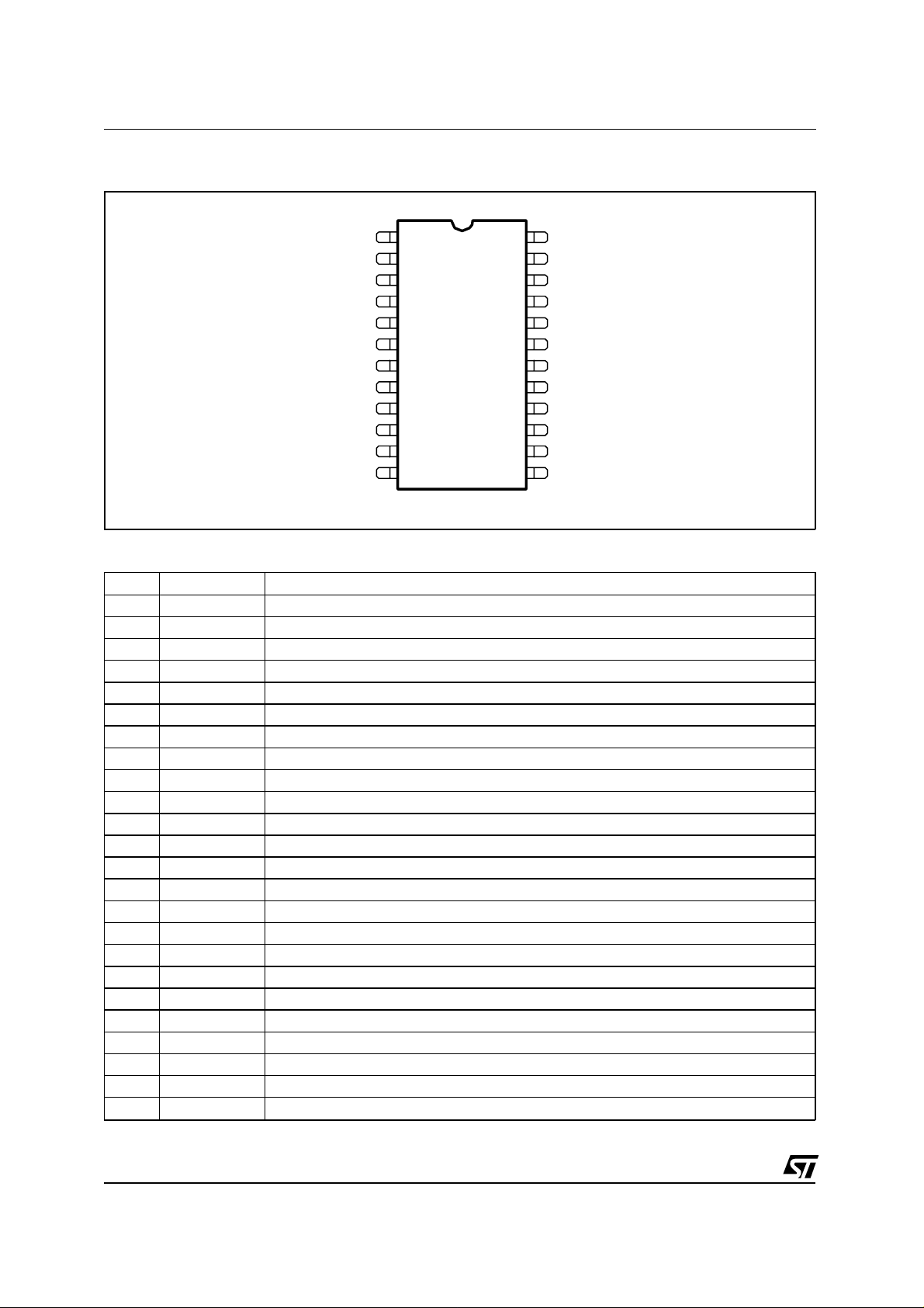
L6660
PIN CONNECTION SO24-SHIRINK (Top view)
A and B
GND-P
COIL
A or B.
OUT1-A
OUTK-A
SLEEP
INA(inv)
INA(not inv) INB(not inv)
V
OSH
Vin 0-5 Vref IN11 14
2
3
4
5
6
7
8
9
10
PINCON
24
23
22
21
20
19
18
17
16
15
1312GND-A V ref OUT
HVP1
HVM
RC comp
V
FDB
V5/12-AP
OUT1-B
OUTK-B
INB(inv)
WENA
PIN FUNCTIONS
N. Name Description
1 AandB MUX Enable (see Tab. 1).
2 GND-P Power ground.
3 COIL Coil for positive step UP and capacitor for negative charge.
4 AorB MUX command Aor B input selection (0 = A; 1 = B).
5 OUT1-A Output ampl.A.
6 OUTK-A Hi current output ampl.A.
7 SLEEP Sleep mode for stand-by condition (0=SLEEP 1=operative).
8 INA (inv) Inverting input of A-amplifier.
9 INA (not inv) Non Inverting input of A-amplifier.
10 Vosh Analog level shifter output Vin-Vref (-2.5 to +2.5 dynamic range)
11 Vin 0-5 Analog level shifter input positive voltage.
12 GND-A Analog ground.
13 V
14 V
15 WENA Multiplexer Enable, Falling Edge sensitive.
16 INB (not inv) Non Inverting input of B-amplifier.
17 INB (inv) Inverting input of B-amplifier.
18 OUTK-B Hi current output ampl.B.
19 OUT1-B Output ampl.B.
20 V5/12-AP Analog&Power voltage supply 5 to 12V.
21 Vfdb Feedback voltage for HVP regulator.
22 RC comp DC-DC converter compensation network.
23 HVM Negative High voltage generated op. amp. supply.
24 HVP Positive High voltage generated op. amp. supply.
OUT Precise 2.5V reference voltage.
ref
IN Input for external reference voltage.
ref
2/9
L6660
ABSOLUTE MAXIMUM RATINGS
Symbol Parameter Value Unit
V512 Supply voltage pin 17 referred to Ground 14 V
HVP Positive high voltage referred to HVM 75 V
HVM Negative high voltage referred to Ground -38 V
IN A&B Amplifier input voltage common mode
V Maximum difference between pin 20 and pins 8, 9, 16 & 17 17 V
∆
T
amb
T
stg
All the voltage value are referred to ground unless otherwi se spec i fied.
Operative Ambient Temperature -20 to +80 °C
Storage Temperature -40 to +125 °C
ELECTRICAL CHARACTERISTICS
(All the following parameters are specified @ 27°C and V5/12 = 12V ±5%, unless otherwise specified.)
Symbol Parameter Test Condition Min. Typ. Max. Unit
V
5/12
HVP
HVripple HVP, HVM ripple
I, hvp Output current (see figure 1)
I, hvm
T
op
F
switch
R
ds, on
I
boost
V
sup
DC gain OpAmp DC gain 130 dB
GBW OpAmp Gain Bandwidth
DCinp OpAmp Input dynamic voltage Double supply -3.5 4.5 V
V
out
DC, I
I
(3) OpAmp Dynamic Output
out
PSRR,P OpAmp Positive power supply
PSRR,N OpAmp Negative power supply
C
load
C
int
K OpAmp Current ratio
Main power supply 4.5 13.2 V
(1)
Output positive Voltage Double Supply Voltage V
Double Supply Voltage V
Single Supply Voltage V
Single Supply Voltage V
512
512
512
512
≥ 8
< 8
≥ 8
< 82718
27
18
External filter cap. 100nF
Characterized only, Not Tested
Time to operating condition 5 ms
(2)
Switching Frequency Refer to Block diagram
I
= 0mA 0.8 V
LOAD
page1/10
Boost transistor ON resistance 4
Boost transistor current limiting 850 mA
Minimum OpAmp supply
Voltage (HVP if externally
given)
Double Supply V512
+4
Single Supply V512
+4
Cload 0.4nF to 24nF
product
Double Supply Voltage
Single supply 1.2 5 V
OpAmp Output dynamic voltage Capacitive load HVM HVP V
OpAmp Bias supply current
bias
|HVP| = |HVM| = 35V 9 mA
(both)
-75 +75 mA
Average current with external
supply
@ 50kHz not tested in production -50 dB
rejection ratio
@ 50kHz not tested in production -50 dB
rejection ratio
OpAmp Load capacitance
Voltage mode Gain min 20dB 0.4 24 nF
range
OpAmp Integration capacitance Charge mode Gain min 20dB 0.4 24 nF
9.8 10 10.2
OUTK/OUT1
6V
±
35
35
70
35
V
V
V
V
300 kHz
Ω
V
V
500 KHz
3/9

L6660
ELECTRICAL CHARACTERISTICS
(continued)
Symbol Parameter Test Condition Min. Typ. Max. Unit
Vout0 OpAmp Output Voltage with 0V
Input Voltage
OUT Reference Voltage PIN13 2.4 2.5 2.6 V
V
ref
Reference Vol tage Outp ut Curren t -1 +1 mA
Filter capacitor at PIN13 10 100 nF
Voltage shift value
(V
PIN11
- V
PIN10
)
V
ref, cap
V
I
vref
shifted
Shifter Gain Analog Voltage Shifter DC
Voltage Gain
V
∆
10
V
∆
11
BW
Vshift
V
IN External reference voltage
ref
Shifter circuitry Band Width 3dB amplitude drop 2 MHz
External feedback programmed
for DC gain value <30V/V
1.0V ≤ Vin0-5 ≤ 3.5V V
V
V
G
PIN11
PIN11
V’’
=
= V
= V
10
0.1
− V’
→ V’
REFIN
+ 0.1V → V"
REFIN
10
10
10
-1 +1 V
IN
V
ref
-2%
IN V
ref
ref
+2%
IN
0.975 1.00 1.025
2.0 2.6 V
(PIN14)
I
sleep
EAoff DC-DC converter Error
Total current in Sleep Mode PIN7 at 0 logic 800
IN = 2.25V -12 +12 mV
V
ref
Amplifier Input voltage Offset
(V
PIN14-VPIN21
I
EA
Error amplifier Current
)
100
±
Capability
HVP% Total HVP precision V
V
logic0
Voltage level for 0 logic at
= 2.25V±0% -4 +4 %
ref
0.9 V
digital input pin (Pin 1-4-7-15)
V
logic1
Voltage level for 1 logic at
1.6 V
digital input pin (Pin 1-4-7-15)
Z
time
T
op
Decay period for ∆V = |19V| V
Operative period from Not
(Pin14) = 2.25V See Fig. 3
ref
0°C < T
case
< 80°C
140 340
4
Selected phase to Selected
phase for each driver
Note 1: Selectable by external resisto rs.
Note 2: Set by external Coil and Capacitor from 80 to 550KHz.
Note 3: Take into account the total power dissipation.
OPERATIONAL AMPLIFIERS DESCRIPTION
Each driver has two output stages scaled in cur-
Figure 1. Load Regulation
36
34
32
10V
9V
8V
12V
11V
rent by a factor K = 10.
In voltage mode configuration the two out puts ar e
shorted.
In charge mode configuration OUT1 drives a capacitor Cint and is closed in feedback, while
OUTK drives the piezo, mirroring the current supplied to Cint, with a current multipl ied by a K fac-
30
28
7V
tor (see Fig.2).
The supply voltage can be internally generated
by the DC-DC converter, or external, maintaining
the DC-DC converter in sleep mode (PIN3
HVP V oltage
26
6V
shorted to ground), in this case the supply voltage can be 0 to V5/12+4 minimum value up to
24
22
59
1
13 17 21 25 29 33 37 41 45 49 53 57 61 65
5V
Load DC C urrent (mA)
70V in single supply or V5/12+4 to 35V symmetrical to ground.
The drivers have 130dB DC gain and the Bandwidth is 500KHz. Stability is guaranteed with a
minimum gain of 20dB, for a capacitive load in
the range 0.4nF up to 24nF.
V
A
µ
A
µ
s
µ
s
µ
4/9

L6660
The drivers can be supplied with HVP-HVM (double supply mode) or with HVP-Ground (single
supply mode). In both cases they can achieve a
rail-to rail output dynamic range with an average
In double supply mode the input stage has 5V/+5V common mode dynamic range, while in
single supply configuration it has 1.2V up to 10V
input common mode dynamic range.
load current up to ±75mA.
Figure 2. Charge Mode Configuration (configuration example; the final application depends on
user needs according with Electrical Characteristics).
Qpiezo=K*[Cint*(1+Ra/Rb)+C]*Vdac
Qpiezo=Cost*Vdac
Cost=k*[Cint*(1+Ra/Rb)+C]
K
Cpiezo
K
Cint
D98IN970A
R
P
Vdac
Rb
HVP
+
-
HVM
Ra
C
1
1
Input Multiplexer
MULTIPLEXER is controlled by internal logic with 3 digital inputs, supplied by IntVref (2.5V), it is compatible to 3.3V and 5V logic command signals, it allows to perform the following configuration:
Table 1.
AandB
(PIN1)
AorB
(PIN4)
0 1 X INA+
0 0 X INA+
1 1 1 INA+
1 0 1 INA+
1 1 (F.E.) INA+
1 0 (F.E.) INA+
WENA
(PIN15)
INA+Status INB+Status Comment
connected to AGND
connected to PIN9
connected to PIN9
connected to AGND
connected to PIN9
connected to AGND
INB+
connected to AGND
INB+
connected to PIN16
INB+
connected to AGND
INB+
connected to PIN16
INB+
connected to AGND
INB+
connected to PIN16
Both drv. inp. are disconnected from ext
PIN and are connected to AGND
Both drv. inp. are accesible
(MUX is transparent)
INA is selected
INB is selected
From WENA Falling Edge, changes on
AorB (pin 4) will not change MUX state.
From WENA Falling Edge, changes on
AorB (pin 4) will not change MUX state.
F.E. = Falling Edge
The MUX is at NOT inv. Inputs, and NO current flows through the MUX switches, because the driver in-
put stage is designed with high impedance stage.
5/9

L6660
Figure 3. Not selected driver return to Zero Output voltage. Both drivers have the same behavior.
The device is in operative condition and AandB (Pin1) and WENA (Pin15) are at 1 logic
condition. The external feedback programmed for a DC gain value <30V/V.
Drivers
OUTPUT
Voltage
+20V
Deselected
Driver Output
Voltage
+2V
0
t
AorB
(PIN4)
AorB
PIN4
(
Drivers
OUTPUT
Voltage
-2V
Ztime
)
Ztime
0
t
Deselected
Driver Output
Voltage
6/9
-20V

L6660
Not selected Output return to 0V
Using the Multiplexer features and selecting just
one driver, the second one, leaves its output voltage and "goes" to 0V (have showed in Fig. 3) , in
"long time" with controlled slope see table 1.
Voltage reference
An internal 2.5V voltage reference generator is
connected to PIN13 (VrefOUT); it is based on an
internal Band-Gap reference with a total precision
of ±4% and a current capability of ±1.0mA, it is always present even in sleep mode condition.
This voltage is used to supply the internal MUX
logic, allowing both 3.3V or 5V logic input signals,
also the internal bias current is based on this reference.
The DC-DC converter reference voltage comes
from PIN14 (VrefIN), so that the user can use an
external voltage reference (from 2.0V up to 2.6V)
or the internal one, in this case, just shorting together VrefOUT and VrefIN (PIN13 and PIN14).
Voltage Shifter
A voltage shifter is inserted to allow a ground
symmetrical driving voltage on the piezo, starting
from a positive (0V up to 5V) input signal coming
from a positive supplied DAC. The DC Input-Output typical tranfer function is plotted in Fig. 4.
This
block works only in Double Supply mode, obviously it doesn’t work if no negat ive supply is present. The voltage shifter out put has not DC-current capability.
For more details see the application note.
DC-DC CONVERTER DESCRIPTION
The DC-DC converter inside t he c hip c an be supplied from 5V up to 12V and has two parts, one to
supply the positive and one to supply the negative voltage.
The DC-DC converter loop "measures" the HVP
voltage by the EXTERNAL voltage divider and
Figure 4. Shifter DC transfer function
Vos h
PIN10
IN,MAX
V
- VrefIN
0
VrefIN
V
IN,MAX
Vin0-5
PIN11
PIN21. The HVP voltage is programmed by two
external resistors as shown in the block diagram,
its value is:
R
V
HVP
V
=
PIN21
⋅ (1 +
fdb1
)
R
fdb2
The DC-DC control loop precision will be improved lower than ±4% respect external reference voltage and resistor voltage divider.
In Sleep Mode HVM is short ed to GND. When in
single supply, HVM must be connected to GND.
The topology is a standard resonant full-wave
boost one:
the LC oscillation is kept running all
the time and a set of comparators is used to synchronize turning on and off of the power MOS in
order to have zero current and zero voltage
switching and furthermore controlled rectification.
The step-up converter is designed to work in Linear mode, and an
AC compensation network is
required (RC-comp) to guarantee the s tabilit y in a
wide operative range (i.e. changing coil, load,
output and input voltage...).
According to the ouput voltage, the current
loaded into the coil is changing like a Voltage
Loop-Current Controlled system, and in every
pulse there is a regulated power transfer to the
load.
The resonant LC topology has been chosen in order to limit the voltage slew-rate across the coil
within reasonable values and so, to minimize radiation problems.
The negative converter is a simple charge transfer: it is supplied by the positive high voltage and
it capacitively translates this positive voltage
down to a negative one, obviously to limit radiation problems also the charge output has a limited slew-rate; moreover to reduce intermodulation phoenomenas the charge output is
synchronized with the LC oscillations of the resonant boost.
This negative voltage is (not counting drops on
external rectification diodes) in tracking with the
positive one and so the negative output controller
is not required.
If the drivers are supplied by HVP & HVM generated by external power supply
the error amplifier
output has to be connected to V5/12.
In the external supply configuration t he maximum
voltage between HVP and HVM (|HVP| + |HVM|)
must not exceed 70V and maximum voltage between GND and HVM must be lower than 35V.
0-VrefIN
V
IN,MAX
5.0V IF V
=
{
V5/12 - 0.5V IF V
5/12
> 5.5V
≤ 5.5V
5/12
7/9

L6660
mm inch
DIM.
MIN. TYP. MAX. MIN. TYP. MAX.
A 2.00 0.079
A1 0.25 0.010
A2 1.51 2.00 0.060 0.079
B 0.25 0.30 0.35 0.010 0.012 0.014
C 0.10 0.35 0.004 0.014
D 8.35 9.35 0.33 0.37
E 7.60 8.70 0.30 0.34
E1 5.02 6.10 6.22 0.20 0.24 0.244
e 0.65 0.025
k 0˚ (min), 10˚ (max)
L 0.25 0.50 0.80 0.010 0.020 0.031
OUTLINE AND
MECHANICAL DA T A
SSO24 (SHRINK)
8/9
A2 A
0.10mm
.004
Seating Plane
Be
A1
D
1324
E
112
K
L
C
E1
SSO24ME

L6660
Information furnished is believed to be accurate and rel i abl e. However, STMicroel ectronics assumes no responsibility for the consequences
of use of such informati on nor for any infringement of patents or other ri ghts of third parties which may result from its use. No license is
granted by im plica tion or otherw ise under any patent or pa tent right s of STMicr oelectronic s. Speci fication mentioned in this publication are
subject to c hange without notice. Thi s publication super sedes and replaces al l i nformation previously suppl ied. STMicroelectronics products
are not authorized for use as critical components in life support devices or systems without express written approval of STMicroelectronics.
The ST logo is a registered trademark of STMicroelectronics
© 2000 STMicroelectronics – Printed in Italy – All Rights Reserved
STMicroelectronics GROUP OF COMPANIES
Australia - Brazil - China - Finland - France - Germany - Hong Kong - India - Italy - Japan - Malaysia - Malta - Morocco -
Singapore - Spain - Sweden - Switzerland - United Kingdom - U.S.A.
http://www.st.com
9/9
 Loading...