

L6615
HIGH/LOW SIDE LOAD SHARE CONTROLLER
■ SSI SPECS COMPLIANT
■ HIGH/LOW SIDE CURRENT SENSING
■ FULLY COMPAT IBL E W ITH REMOTE
OUTPUT VOL TAGE SENSING
■ FULL DIFFERENTIAL LOW OFFSET
CURRENT SENSE
■ 2.7V TO 22V V
■ 32kΩ SHARE SENSE AMPLIFI ER INP U T
OPERATING RANGE
CC
IMPEDANCE
■ HYSTERETIC U VL O
APPLICATION
■ DISTRIBU TED PO WE R SYSTEMS
■ HIGH DENSITY DC-DC CONVERTERS
■ (N+1) REDUNDANT SYSTEMS, N UP TO 20
■ SMPS FOR (WEB) SERVERS
DESCRIPTION
This controller IC is specifically designed to
TYPICAL APPLICATION DIAGRAM
R
R
R
SENSE
SENSE
+OUT
+OUT
+OUT
+OUT_S
+OUT_S
+OUT_S
-OUT_S
-OUT_S
-OUT_S
-OUT
-OUT
-OUT
PS #1
PS #1
PS #1
+OUT
+OUT
+OUT
+OUT_S
+OUT_S
+OUT_S
-OUT_S
-OUT_S
-OUT_S
-OUT
-OUT
-OUT
PS #N
PS #N
PS #N
SENSE
R
R
R
G1RG2
G1RG2
G1RG2
R
R
R
SENSE
SENSE
SENSE
R
R
R
G1
G1
G1
(*)
(*)
R
R
R
ADJ
ADJ
ADJ
1
1
1
GND
GND
GND
VCC
VCC
VCC
CS-
CS-
CS-
2
2
2
CGA
CGA
CGA
CS+
CS+
CS+
3
3
3
SHARE
SHARE
SHARE
ADJ
ADJ
ADJ
4
4
4
COMP
COMP
COMP
L6615
L6615
L6615
(*)
(*)
R
R
R
ADJ
ADJ
ADJ
R
R
R
G2
G2
G2
1
1
1
GND
GND
GND
VCC
VCC
VCC
CS-
CS-
CS-
2
2
2
CGA
CGA
CGA
CS+
CS+
CS+
3
3
3
SHARE
SHARE
SHARE
ADJ
ADJ
ADJ
4
4
4
COMP
COMP
COMP
L6615
L6615
L6615
BCD TECHNOLOGY
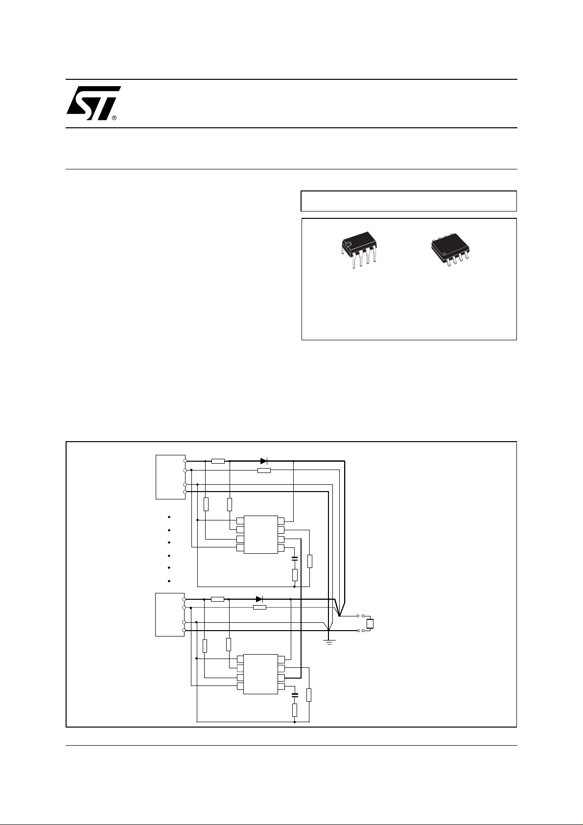
DIP8 SO8
ORDERING NUM BERS :
L6615N L6615D
L6615DTR(T & Reel)
achieve load sharing of paralleled and independent power supply m odules in distributed power
systems, by adding only few external components.
Current sharing is achieved through a single wire
connection (share bus) common to all of the paralleled modules.
8
8
8
7
7
7
6
6
6
5
5
5
C
C
C
C
C
C
R
R
R
CGA
CGA
CGA
R
R
R
C
C
C
+OUT
+OUT
+OUT
LOAD
LOAD
LOAD
GND
GND
GND
SHARE BU S
SHARE BU S
SHARE BU S
8
8
8
7
7
7
6
6
6
5
5
5
C
C
C
R
R
R
R
R
R
CGA
CGA
C
C
C
C
C
C
CGA
(*) OR-ing FET can
(*) OR-ing FET can
be used to reduce
be used to reduce
power dissipation
power dissipation
July 2003
1/20
L6615
DESCRIPTION (continued)
Load sharing is a technique used in all the systems in which the load requires low vol tage, high current
and/or redundancy; for this reason a modular power syst em is necessary in which t wo or more power supplies or DC-DC converters are paralleled.
The device is able to perform both high side and low side current sensing, that is the sense current resistor
can be placed either in series to the power supplies output or on the ground return.
The L6615 then drives the share bus to a voltage proportional to the output current of the master that is
to the highest amongst the output currents delivered by the paralleled power supplies.
The share bus dynamics is independent of the power supply output voltage and is clamped only by the
device supply voltage (V
The output voltage of the other paralleled power supplies (slaves) is then trimmed by the ADJ pin so that
they can support their amount of load current. The slave power supplies work as current-controlled current
sources.
Sharing the output currents is useful for equalizing also the thermal stress of the different modules and
providing an advantage in term of reliability.
Moreover the paralleled supplies architecture allows achieving redundancy; the failure of one of the modules can be tolerated until the capability of the remaining power supplies is enough to provide the required
load current.
PIN DESCRIPTION
N° Pin Function
1 GND Ground.
CC
).
2 CS- Input of current sense amplifier; it is connected to the negative side of the sense resistor through
a resistor (R
3 CS+ Input of current sense amplifier. A resistor (RG1, of the same value as RG2) is placed between
this pin and the positive side of the sense resistor: its value defines the transconductance gain
between I
4 ADJ Output of Adjust amplifier; it is connected to both the load (through a resistor R
positive remote sense pin of the power system. This pin is an open collector diverting (from the
feedback path) a current proportional to the difference between the current supplied to the load
by the relevant power supply and the current supplied by the master.
5 COMP Output of the current sharing (transconductance) error amplifier and input of ADJ amplifier.
Typically , a compensation network is placed between this pin and ground. The maximum voltage
is internally clamped to 1.5V (typ.)
6 SH Share bus pin. During the power supply
share bus. During power supply
proportional to the load current.
share
The
and GND could be useful to reduce the noise present on the share bus.
7 CGA Current Gain Adjust pin; current sense amplifier output. A resistor connected between this pin
8V
and ground defines the maximum voltage on the share bus and sets the gain of the current
sharing system.
Supply voltage of the IC.
CC
).
G2
and V
CGA
bus connects the SH pins of all the paralleled modules. A capacitor between this pin
SENSE
.
) and to the
ADJ
slave
operation, this pin acts as positive input from
master
operation, it drives the share bus to a voltage
2/20
ABSOLUTE MAXIMUM RATINGS
Symbol Pin Parameter Value Unit
L6615
V
CC
ICS+, ICS- Sense pin current 10 mA
VCS-, V
V
(V
All voltages are with re spect to pin 1. C urrents are positive into, negative out of t he specified t erminal.
(*) Maximum package power dissipation limits must be observed
, VSH,
CS+
, V
ADJ
CGA
V
COMP
) - (V
CS+
Ptot Total power dissipation @ Tamb = 70°C
Tstg Storage temperature -55 to +150 °C
) Differential input voltage (VCS+ from 0V to 22V) -0.7 to 0.7 V
CS-
Tj Junction temperature range -40 to +125 °C
8 Supply Voltage (*) (ICC<50mA) selflimit V
2, 3, 6, 4, 7 -0.3 to V
5 Error amplifier output -0.3 to 1.5 V
SO8
DIP8
CC
0.45
0.6
PIN CONNECTION
8
8
VCC
7
7
VCC
CGA
CGA
GND
GND
CS-
CS-
1
1
2
2
V
W
6
CS+
CS+
ADJ
ADJ
3
3
4
4
6
5
5
SH
SH
COMP
COMP
THERMA L D ATA
Symbol Parameter MINIDIP SO8 Unit
R
th j-amb
Thermal Resistance junction to ambient 90 120 °C/W
3/20
L6615
ELECTRICAL CHARACTERISTCS
(Tj = -40 to 85°C, Vcc=12V, V
V
SENSE
= IL * R
, RG1 = RG2 = 200Ω)
SENS E
Symbol Parameter Test Condition Min. Typ. Max. Unit
Vcc
V
V
CC, ON
V
CC,OFF
V
Vz I
Operating range 2.7 22 V
cc
Quiescent current VSH= 1V, V
I
cc
Turn-on voltage VSH= 0.2V, V
Turn-off voltage 2.35 2.5 2.65 V
Hysteresis 100 mV
H
CURRENT SENSE AMPLIFIER
V
V
I
CGAS
I
B(CS-)
I
B(CS+)
CMR Common mode dynamics range V
VTH
SW
Input offset voltage 0.1V ≤ VSH ≤ 10.0V -1.5 0.0 1.5 mV
OS
Out high voltage V
CGA
Short circuit current V
Input bias current (high side
sensing)
Input bias current (low side
sensing)
Switchover threshold low side to
CS+
high side sensing
Switchover hysteresis 0.16 V
H
SHARE DRIVE AMPLIFIER
HV
LV
α
α
V
SH, load
I
SR Slew rate V
SH high output voltage V
SH
SH low output voltage
SH
High side sensing mirror accuracy
(+)
(*)
Low side sensing mirror accuracy
(-)
(*)
Load regulation -1.0mA ≤ I
Short circuit current VSH= 0V, V
SC
= 12V, C
ADJ
= 5nF to GND, R
COMP
= 0V 5 6 mA
SENSE
= 0V 2.45 2.60 2.75 V
SENSE
= 20mA 24 26 V
CC
= 0.25V Vcc-2.2 V
SENSE
= 0V, V
CGA
V
V
V
V
= 0V, V
SENSE
= 0V, V
SENSE
CS-, VCS+
CS+
= 250mV, ISH= -1mA Vcc-2.2 V
SENSE
= 0mV, RSH= 200Ω
CGA
= 0.45V -1.5 -2.0 mA
SENSE
=+12V 1.0 µA
CS+
=0V -1.0 µA
CS+
= 16kΩ, unless otherwise specified;
CGA
0V
CC
1.6 V
45 mV
±1 ±5 %
±1 ±5 %
SDA(OUT)
SENSE
= -10mV to 90mV step,
SENSE
≤ -4mA 20 mV
= 25mV -20 -13.5 -8 mA
0.8 1.5 2.2 V/µs
RSH= 200Ω to GND
V
= 90mV to –10mV step,
SENSE
234V/µs
RSH= 200Ω to GND
V
SHARE SENSE AMPLIFIER
R
Input impedance 22.4 32 41.6
i
ERROR AMPLIFIER
G
V
4/20
Transconductance 3 4 5 mS
m
Input offset voltage V
os
=1V 30 50 70 mV
CGA
Ω
k
L6615
ELECTRICAL CHARACTERISTCS
(Tj = -40 to 85°C, Vcc=12V, V
V
SENSE
= IL * R
, RG1 = RG2 = 200Ω)
SENS E
= 12V, C
ADJ
(continued)
COMP
= 5nF to GND, R
= 16kΩ, unless otherwise specified;
CGA
Symbol Parameter Test Condition Min. Typ. Max. Unit
I
I
Source current V
OH
Sink current V
OL
COMP
V
SENSE
COMP
=1.5V, V
=-10mV
= 1.5V, V
≥ 300mV,
SH
SENSE
=-10mV
-150 -350 -400 µA
100 200 300 µA
200Ω resistor SH to GND
V
COMP(L
V
Low voltage 0.05 0.15 0.25
)
Clamp Zener voltage IZ = 1mA 1.5 V
Z
ADJ AMPLIFIER
I
ADJ
V
R
V
ADJ(MIN)
(*) Mirror accuracy is defined as :
Max. ADJ output current VSH= 1V, V
Threshold voltage I
T
Emitter resistor Guaranteed by design 60 100 140 Ω
A
Low saturation voltage I
----------------------------------------- 1–
V
SENSE
=10µA 0.7 V
ADJ
=5mA 1 V
ADJ
I
=1mA 0.4 V
ADJ
V
SH
R
CGA
---------------
⋅
R
G
= 0V 6.5 10 13 mA
SENSE
100⋅
and it represents the accuracy of the transfer between the voltage sensed and the voltage imposed on the
share bus.
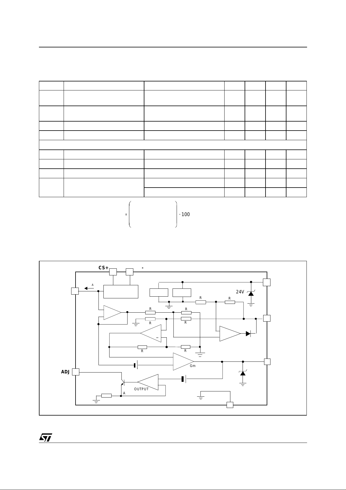
BLOCK DIAGRAM
CGA
CGA
7
7
ADJ
ADJ
4
4
I
I
CGA
CGA
CS+
CS+
CURRENT SENSE
CURRENT SENSE
AMPLIFIER (CSA)
AMPLIFIER (CSA)
+
+
_
_
SHARE SENSE
SHARE SENSE
AMPLIFIER (SSA)
AMPLIFIER (SSA)
R
R
A
A
CS-
CS-
23
23
R
R
40 mV
40 mV
ADJ OUTPUT
ADJ OUTPUT
AMPLIFIER (AOA)
AMPLIFIER (AOA)
R
R
R
R
UVLO
UVLO
+
+
_
_
+
+
_
_
BIAS
BIAS
R
R
R
R
R
R
+
+
_
_
AMPLIFIER (E/A)
AMPLIFIER (E/A)
0.7V
0.7V
R
R
Gm ERROR
Gm ERROR
24V
24V
R
R
_
_
+
+
SHARE DRIVE
SHARE DRIVE
AMPLIFIER (SDA)
AMPLIFIER (SDA)
1
1
GND
GND
1.5V
1.5V
8
8
6
6
5
5
V
V
CC
CC
SH
SH
COMP
COMP
5/20
L6615
Figure 1. Turn- o n and turn-off voltage
V
, V
CC(OFF)
[V]
CC(ON)
3
2.6
2.2
-50 0 50 100
TJ [OC]
Figure 2. Supply current vs. supply voltage
ICC [mA]
100
10
Figure 4. Max CGA current
I
[mA]
CGA(max)
2.8
2.6
2.4
2.2
2
1.8
-50 0 50 100
TJ [
O
C]
Figure 5. High side/low side sensing
switchover thresh old
VTH [V]
1.9
1.7
1
0.1
0.01
0.1 1 10 100
V
[V]
CC
Figure 3. Supply current
ICC [mA]
4.7
4.3
3.9
3.5
3.1
2.7
-50 0 50 100
TJ [
O
C]
1.5
1.3
-50 0 50 100
O
TJ [
C]
Figure 6. Max. share bus voltage at no load
V
[mV]
SH(LOW)
50
45
40
35
30
25
20
15
10
-50 0 50 100
TJ [OC]
6/20
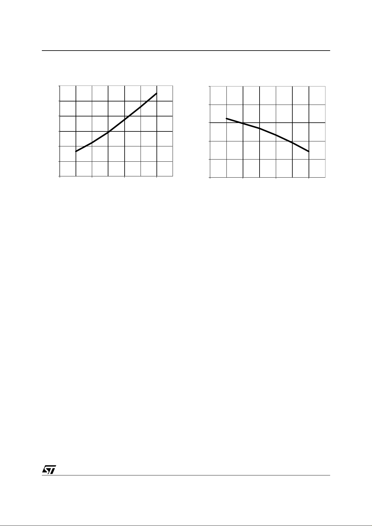
Figure 7. Share bus input impedance Figure 8. ADJ maximum current
RI [k ]
50
I
ADJ[MAX]
15
[mA]
L6615
45
40
35
30
25
20
-50 0 50 100
TJ [
O
C]
13
11
9
7
5
-50 0 50 100
TJ [
O
C]
7/20

L6615
APPLICATION INFORMATION
Index page
1. Introduction 8
2. Curren t sense section 9
3. Share drive section, error amplifier and adjust amplifier 10
4. Designing with L6615 10
5. Curren t sense methods 13
6. Application ideas 14
7. Low voltage buses 15
8. O ffset Trimming 16
1 INTRODUCTION
Power supply systems are often designed by paralleling converters in order to improve performance and
reliability.
To ensure uniform distribution of stresses, the total load current should be shared appropriately among
the converters.
A typical application is showed in fig. 9 for a series of N paralleled modules (PS#1 to PS#N): each of them
exhibits 4 terminals: two for the power output (+OUT, -OUT) and two for the remote sense signals
(+OUT_S, -OUT_S).
On the power lines are placed the sense resistors R
(to avoid that the failure of one module shorts the load out)
L6615 allows attaining an automatic master-slav e current sharing architecture: one L6615 i s associated to each
power supply and all these IC's are linked each other through the share bus (referred to the common ground).
This kind of system configuration is preferred to the systems in which a single current sharing controller is
used because of robustness, reliability and flexibility.
To configure a load share controller, few passive components are used. A brief device explanation will
follow with the formulas useful to set these external components.
(for the current sensing) and the OR-ing diodes
SENSE
Figure 9. Typical high side connection
R
R
SENSE
+OUT
+OUT
+OUT_S
+OUT_S
-OUT_S
-OUT_S
-OUT
-OUT
PS #1
PS #1
+OUT
+OUT
+OUT_S
+OUT_S
-OUT_S
-OUT_S
-OUT
-OUT
PS #N
PS #N
SENSE
R
R
G1RG2
G1RG2
R
R
SENSE
SENSE
R
R
G1
G1
R
R
ADJ
ADJ
1
1
VCC
GND
VCC
GND
CS-
CS-
2
2
CS+
CS+
3
3
ADJ
ADJ
4
4
R
R
G2
G2
1
1
GND
GND
CS-
CS-
2
2
CS+
CS+
3
3
ADJ
ADJ
4
4
L6615
L6615
R
R
ADJ
ADJ
SHARE
SHARE
L6615
L6615
CGA
CGA
SHARE
SHARE
COMP
COMP
VCC
VCC
CGA
CGA
COMP
COMP
8
8
7
7
6
6
5
5
8
8
7
7
6
6
5
5
C
C
C
C
R
R
C
C
C
C
C
C
R
R
C
C
R
R
CGA
CGA
SHARE BUS
SHARE BUS
R
R
CGA
CGA
+OUT
+OUT
GND
GND
LOAD
LOAD
8/20

L6615
2 CURRENT SENSE SECTION
A sense resistor is typically used to generate the voltage drop, proportional to the load current, measured
by the CSA (Current Sense Amplifier), whose input pins (pins #2 and #3) are connected across of R
through two identical resistors (RG1 and RG2).
The CSA consists of 2 s ections (see fig. 1 0), on e respons ible fo r the h igh side sens ing, th e other fo r low
side sensing. An internal comparator activates the relevant section in accordance with the voltage present
at CS+ pin: if this voltage is higher t han 1.6V (typ), then the hi gh side sensing section will be a ctivated
(fig10.a) otherwise the low side sensing one will (fig 10.b). For the sake of simplicity we will consider R
R
= RG.
G2
As the voltage drop I
OUT*RSENSE
is present at the input of the Sense Amplifier section, its output forces
the controlled current mirror to:
– sink current from the CS+ pin in case of high side sensing (neglecting input bias current, no current flows
through CS- pin);
– source current from th e CS- pin in case of l ow side sensing (neglecting inpu t bias current, no c urrent
flows through CS- pin).
The local feedback imposes the same v oltage at the cu rrent sense inp ut pins , so under closed loop condition V
SENSE
=VRG.
The current
I
⋅
I
CS
OUTRSENSE
-------------------------------------- -=
R
G
SENSE
G1
=
(ICS+ in case of high side, I
ing a drop across the R
in case of low side) is then internally mirrored and sent to the CGA pin caus-
CS-
external resistor: two internal buffers transfer V
CGA
V
SNS
SH
--------------
V
R
⋅=
R
G
CGA
signal on the share pin so:
CGA
Only the L6615 VCC limits the upper voltage at the CGA and SH pin, independently of the voltage present
at the current sense pins.
In noisy applications, two capacitors of small value (e.g. 1nF) connected between current sense pins and
ground could be useful to clean the signal at the input of the current sense amplifier.
For low voltage buses application, see paragraph 7.
Figure 10. Current sense section
LOAD(-) / GND
LOAD(-) / GND
R
R
I
I
OUT
OUT
V
SENSE
SENSE
PS-
PS-
V
V
V
R
R
G
G
SENSE
SENSE
RG
RG
R
R
CSA
CSA
+
+
HSA
CS+
CS+
CS-
CS-
G
G
HSA
-
-
CGA
L6615
L6615
CGA
I
I
CGA
CGA
R
R
CGA
CGA
COMPARE
COMPARE
1.6V
1.6V
-
-
LSA
LSA
+
+
SOURCE
SOURCE
I
I
CS-
CS-
CONTROLLED
CONTROLLED
CURRENT
CURRENT
MIRROR
MIRROR
1:1
1:1
I
I
OUT
OUT
R
R
SENSE
SENSE
LOAD(+)
LOAD(+)
PS+
PS+
V
V
R
R
V
V
SENSE
SENSE
R
R
I
I
CS+
G
G
CS+
CS+
RG
RG
CS-
CS-
G
G
CS+
SINK
+
+
HSA
HSA
-
-
COMPARE
COMPARE
1.6V
1.6V
-
-
LSA
LSA
+
+
SINK
1:1
1:1
CONTROLLED
CONTROLLED
CURRENT
CURRENT
MIRROR
MIRROR
CSA
CSA
L6615
L6615
CGA
CGA
I
I
CGA
CGA
R
R
CGA
CGA
a) high side sensing b) low side sensing
9/20

L6615
3 SHARE DRIVE SECTION, ERROR AMPLIFIER AND ADJUST AMPLIFIER
The gain between the output of CSA (CGA pin) and output of SDA (SH pin) is 1 (typ.) so, for the master
power supply, V
In the slave converters, being V
diagram) isolates the output this amplifier from the share bus.
The Share Sense Amplifier (SSA) reads t he bus v ol tage transferring the sig nal t o the non-i nverting input
of the error amplifier where it is compared with CGA voltage.
Whenever a controller acts as the master in the system, the voltage difference between the E/A inputs is
zero. To guarantee its output low in such condition, a 40mV offset is inserted in series with the inverting
input.
Instead in the slave converters the inp ut voltage difference is pro portional to the differenc e between the
master load current and the relevant slave load current.
The transconductance E/A converts the ∆V at its inputs in a current equal to
flowing in the compensation network connected between COMP pin and ground.
The E/A output voltage drives the adjust amplifier to sink current from the ADJ pin that is connected to the
output voltage through a small resistor along the sense path. The current sunk by ADJ pin is deviated from
feedback path of the slave power supply tha t reac ts increasing its duty cycle.
In steady state the current sunk by the ADJ pin is proportional to the value of error amplifier output.
= VSH; the voltage on the share bus is imposed by the master.
CGA
CGA(SLAVE)
< V
CGA(MASTER)
I
OUT
GM∆V⋅=
, the diode at the output of SDA (see block
4 DESIGNING WITH L6615
The first design step is usually the choice of the sense resistor whose maximum value is limited by power
dissipation; this constraint must be traded off against the precision of L6615 current sensing. In fact a small
sense resistance value lowers the power dissipation but reduc es t he signal available at the inputs of t he
L6615 current sense amplifier.
Once fixed R
specs: usually these specs define the share bus voltage (V
then the values for RG and R
SENSE
will be chosen in acc ordance with the appl ication
GCA
SH(MAX)
) and the number of paralleled power
supp li es.
Their value must comply with the constraints imposed by the L6615:
Figure 11. Simplified feedback block diagram.
I
I
R
R
α * R
α * R
--
--
OUT(2)
OUT(2)
SENSE
SENSE
CGA
CGA
/ R
/ R
POWER
POWER
STAGE 2
STAGE 2
G
G
PWM
PWM
CONTROLLER
CONTROLLER
POWER
POWER
STAGE 1
STAGE 1
PWM
PWM
CONTROLLER
CONTROLLER
R
R
α * R
α * R
I
I
OUT(1)
OUT(1)
SENSE
SENSE
CGA
CGA
V
V
OUT
OUT
Z
Z
L
L
SHARE BU S
/ R
/ R
G
G
SHARE BU S
+
+
Σ Σ
Σ Σ
I
I
LOAD
LOAD
+
+
10/20
+
-
-
K*V
K*V
Σ
Σ
OUT
OUT
+
V
V
REF
REF
(*)
(*)
+
GM*Z
(s)*R
GM*Z
GM*Z
GM*Z
COMP
COMP
R
R
(s)*R
(s)*R
A
A
ADJ
ADJ
(*) K depends on the
(*) K depends on the
feedback divid er ratio
feedback divid er ratio
K*V
K*V
Σ
Σ
OUT
OUT
+
+
-
-
(*)
(*)
+
+
V
V
REF
REF
COMP
COMP
R
R
(s)*R
A
A
ADJ
ADJ
+

L6615
– maximum share bus voltage is internally limited up to 2.2V below L6615 VCC voltage (pin#8);
–V
SH(MAX)
keeping in mind that every Vol t on the share bus wil l increase the master c ontroller's suppl y current
by approximately 4 5 µA for eac h s lave un it c onnect ed in paral lel; t his tot al current , prov ided by t he
master share drive amplifier, must be lower than its minimum output capabilty (8mA) so
This condition is not tough t o meet in normal applications, as one can easily see by us ing sensible
values for N (number of paralleled power supplies) and V
solving for N, we obtain Nmax=20;
– maximum share drive amplifier current capability (I
– for safety reasons the following relation must be met:
represents an up per limit but the designer should select the fu ll scale share bus voltage
R
iMIN()
V
SH MAX()
R
G
-------------------
V
1
out
---
---------------- 40–
⋅>
2
10mA
N
CGA(MAX)
8mA⋅<
SH(MAX)
=2mA);
. For example, with V
SH(MAX)
=8V,
in this way no fault will cause I
At full load, ∆V
R
I
OUT(MAX)
(typically few hundreds of millivolt).
SENSE
SENSE(MAX)
is the maximum current carried by each of the paralleled power supply; in non redundant sys-
= I
OUT(MAX
CS+
(or I
) · R
SENSE(MAX)
) to overcome its absolute maximum ratings.
CS-
is the maximum voltage drop across the resistor
tems composed by N power supplies, each of them works at its nominal current, so:
I
I
OUT MAX()
LOAD
--------------- -=
N
This relationship is true also in N+M redundant system, even if under normal condition each power supply
provides I
LOAD
/(N+M).
For example in a system composed by two paralleled power supplies 100% redundant (N=M=1), each
module is sized to sustain the entire load current (in normal operation it carries only one half): for this reason the sense resistor must be sized considering the whole load current.
The temperature variation of the sense resisto r (hence of its resistance value) has to be taken into account, so R
Once fixed V
SENSE(MAX)
SENSE(MAX)
is the value at maximum operating temperature to avoid saturating the share bus.
, the r a tio R
CGA/RG
(gain from the sens ing section to t he s hare bus ) can be cal-
culated:
where V
SH(MAX)
is defined by the application.
A small capacitor in parallel to R
R
CGA
---------------
R
G
is useful to reduce the noise.
CGA
V
SH MAX()
-------------------------------------=
V
SENSE MAX()
The effect of current sharing feedback loop is to force the voltages of the slave's CGA pins to be equal to
V
(that is to reduce the voltage difference a t the inputs of the L6615 error amplifier). For the sake of
SH
simplicity we consider 2 paralleled power supplies (as in fig. 11): under closed loop condition:
I
OUT 1()
R
SNS 1()
--------------------- -
⋅⋅ I
R
G1()
R
CGA 1()
OUT 2()
R
SNS 2()
--------------------- -
⋅⋅=
R
G2()
R
CGA 2()
Ideally all the external component and α are matched so:
I
LOAD
I
OUT 1()IOUT 2()
--------------- -==
2
Any mismatch will have repercussion on the sharing precisio n: in particular the maximum di fference between the output currents (sharing error) will be given by the sum of the mismatches amongst the relevant
values.
11/20

L6615
Figure 12. ADJ network
V
V
OUT
OUT
R
R
ADJ
ADJ
R
R
E/A
E/A
V
V
REF
REF
To set the R
(V
±∆VO); the maximum difference between master and slave output voltage is 2*∆VO and this amount
OUT
value it is necessary to know the tolerance required of the po wer supply output voltage
ADJ
I
I
ADJ
ADJ
to L6615
to L6615
ADJ pin
1
1
a) b)
a) b)
ADJ pin
R
R
2
2
Off the shelf
Off the shelf
POWER SUPPLY
POWER SUPPLY
E/A
E/A
V
V
OUT
OUT
R
R
ADJ
ADJ
V
V
REF
REF
I
I
ADJ
ADJ
to L6 615
to L6 615
ADJ pin
ADJ pin
represents the voltage that the L6615 must be able to correct.
Now two different approaches are feasible depending on whether the SMPS (whose out put current must
be shared) has to be completely designed or it is an "off the shelf" component and only the current sharing
section must be designed.
In the first case, the adjustment resistor (R
feedback divider R
(see fig.12.a): typically the first step consist of fixing the current flowing, under steady
H
state condition, through the feedback divider I
) can be considered as a fraction of the high resistor of the
ADJ
; by choosing the value for R2:
FB
V
I
FB
--------------=
REF
R
2
we will have:
V
R
H
It can be an useful rule of thumb to use R
R1R
+
ADJ
lower than (or equal to) one tenth of R1, considering that, in
ADJ
OUT
-------------- - 1–
V
REF
R
⋅==
2
worst cas e condition, it will b e:
V
∆
I
ADJ max()
OUT
------------------=
R
ADJ
This value must not exceed the one indicated in the "Electrical characteristic section" but this is very easy
to meet, as one can easily see by using sensible values for ∆V
OUT
and R2.
In the second case (fig 12.b), the feedback divider has been already designed by the SMPS manufacturer
and it is not possible to modify it: the design of R
maximum spread without signif icantly s hifting t he SMP S regul ati on poi nt. A m inimum R
must be done to make the L6615 able to correct the
ADJ
value can be
ADJ
found by:
V
∆
OUT
------------------------- -=
I
ADJ max()
where I
ADJ(max)
is 8mA.
R
ADJ min()
Especially for low voltage output buses it is important to avoid adjustment network saturation; the design
must satisfy the follo wing relationship:
where V
ADJ(MIN)
V
OUTRADJIADJIFB
can be found in the "Electrical characteristic section" for different I
+()V
>⋅–
ADJ MIN()
ADJ
values.
12/20

L6615
The last point is the des ign of the com pensation network ZC(s) connected between the COMP pin and
ground.
Besides the power supply feed back loop, the current shari ng system introduces anot her, outer loop. T o
avoid interaction between them it is important to design the bandwidth of the sharing loop at least one order of magnitude lower than the bandwidth of the power supply loop.
For the total system, th e loop gain is:
R
CGA
G
LOOP s()RSENSE
---------------
R
G
G
MZC
where
A
(s) is the transfer function of PWM controller and power stage (see fig. 11)
PWR
R
is the equivalent load resistance
LOAD
Typically the compensation network is built by a R-C series.
A resistor in series with C
at the load share loop crossover frequency, f
If f
is the share loop crossover frequency, then:
C(SH)
is required to boost the phase margin of the load share loop. The zero is placed
C
------------------------------- -
C
C
2πf
1
⋅⋅
⋅⋅⋅⋅=
CSH()
R
CGAGM
---------------------------- -
C(SH)
R
G
.
R
⋅
ADJ
------------- -
R
s()
A
R
ADJ
------------- -
R
A
R
SENSE
--------------------- -
R
LOAD
A
PWR
A
PWR f
1
------------------
⋅⋅⋅⋅⋅⋅=
s()
R
LOAD
()
CSH()
-------------------------------------------- -=
R
C
2πf
1
⋅⋅ ⋅
CSH()
C
C
5 CURRENT SENSE METHODS
Several are the metho ds to sense the p ower supply output c urrent; the simplest one i s to use a power
resistor (fig. 13a) but increasing load current could require expensive resistor to support the inherent power dissipation, imposing the use of several paralleled resistor.
Other methods to sense the output current are showed in fig. 13b and 13c:
1. R
as sense resistor (fig 13a): the L6615 sense pins will be connected, through R
: a power MOS is placed in series to the output and its channel resistance (R
DS(ON)
) is used
DS(ON)
resistors to the drain
G
and to the source of the M OS. Beside s p roviding the s ense res istor, the F ET is used as "ORi ng" element: driving properly its gate, it is possible isolate the power supply output from the load (the body
diode is reversed biased so it doesn't conduct).
This is useful whenever features like hot swap or hot plug are required; compared with the well-known
solution using ORing diode, the ORing FET greatly reduces the power dissipation, in particular:
2
⋅+⋅=
where V
P
DIODE()
P
MOS()
is the forward drop across the diode.
F
V
I
F
OUTRSENSEIOUT
R
DS O N()IOUT
2
⋅=
2. Current transformer: in case of very high load currents, a transformer allows s ensing a smaller cur-
rent, obtained through a s caling factor equal t o the transformer turn ratio. In this way , t he se nse resistor power dissipation requirements can be less tight: obviously this is paid with the cost of the
transformer.
In fig. 13c it is showed the simplified output stage of a power supply in forward configuration: through
two current transformers the load current is reproduced in the sensing circuit scaled by a factor N.
R
will read a ripple (at the switching frequency) superimposed on the average curren t value
SENSE
that doesn't affect the correct behaviour of the current sharin g system because its loop gain is designed with a low bandwidth - at least 2 order of magnitude lower than the switching frequency - that
will cut this high frequency.
13/20

L6615
Figure 13. Current sense methods.
L6615
L6615
CS+ CS-
CS+ CS-
R
R
G
G
L
L
O
O
A
A
D
D
POWER
POWER
SUPPLY
SUPPLY
POWER
POWER
SUPPLY
SUPPLY
R
R
G
G
R
R
SNS
SNS
I
I
OUT
OUT
L6615
L6615
CS+ CS-
CS+ CS-
R
R
G
G
ORing FET
ORing FET
I
I
OUT
OUT
GATE
GATE
CONTROL
CONTROL
CS+
CS+
R
R
G
G
L6615
R
R
SNS
SNS
1:N
1:N
1:N
R
R
G
G
L
L
O
O
A
A
D
D
1:N
L6615
R
R
CS-
CS-
G
G
SENSING
SENSING
CIRCUIT
CIRCUIT
I
I
OUT
OUT
L
L
O
O
A
A
D
D
a)
b)
c)
6 APPLICATION IDEAS
In fig. 14 is showed a single sect ion of a system in which several DC to DC modu les can be paral leled,
typical solution whenever the load requires high current at low voltage; the converter is designed for a step
down configuration using a synchronous rectification controller (for example L6910 [1] or L6911 [2] ST device).
The L6615 reads the drop acros s th e Rds( ON) of t he O R -ing FET and the LM2 93 drives it s gat e, pull ing
it down whenever a fault condition (e.g. short on the low side) appears.
A charge pump could be necessary to be sure that the ORing FET V
is higher than V
GS
GS(TH)
(depending
on the input and output voltage).
Figure 14. 0.9 to 5V DC-Dc converter with Current Sharing and output hot-pluggability
VIN
VIN
4
4
7
7
6
6
VOUT
VOUT
VCC
VCC
BOOT
BOOT
UGATE
UGATE
PHASE
PHASE
8
8
5
5
LM293
LM293
14/20
GND
GND
SS
SS
COMP
COMP
L6910
L6910
LGATE
LGATE
PGND
PGND
VFB
VFB
+S_OUT
CS-
L6615
L6615
CGA
CGA
CS-
Vcc
Vcc
SH
SH
CS+
CS+
ADJ
ADJ
GND
VIN
VIN
Q1R1
Q1R1
GND
COMP
COMP
+S_OUT
SH
SH
-SOUT
-SOUT
P_GND
P_GND
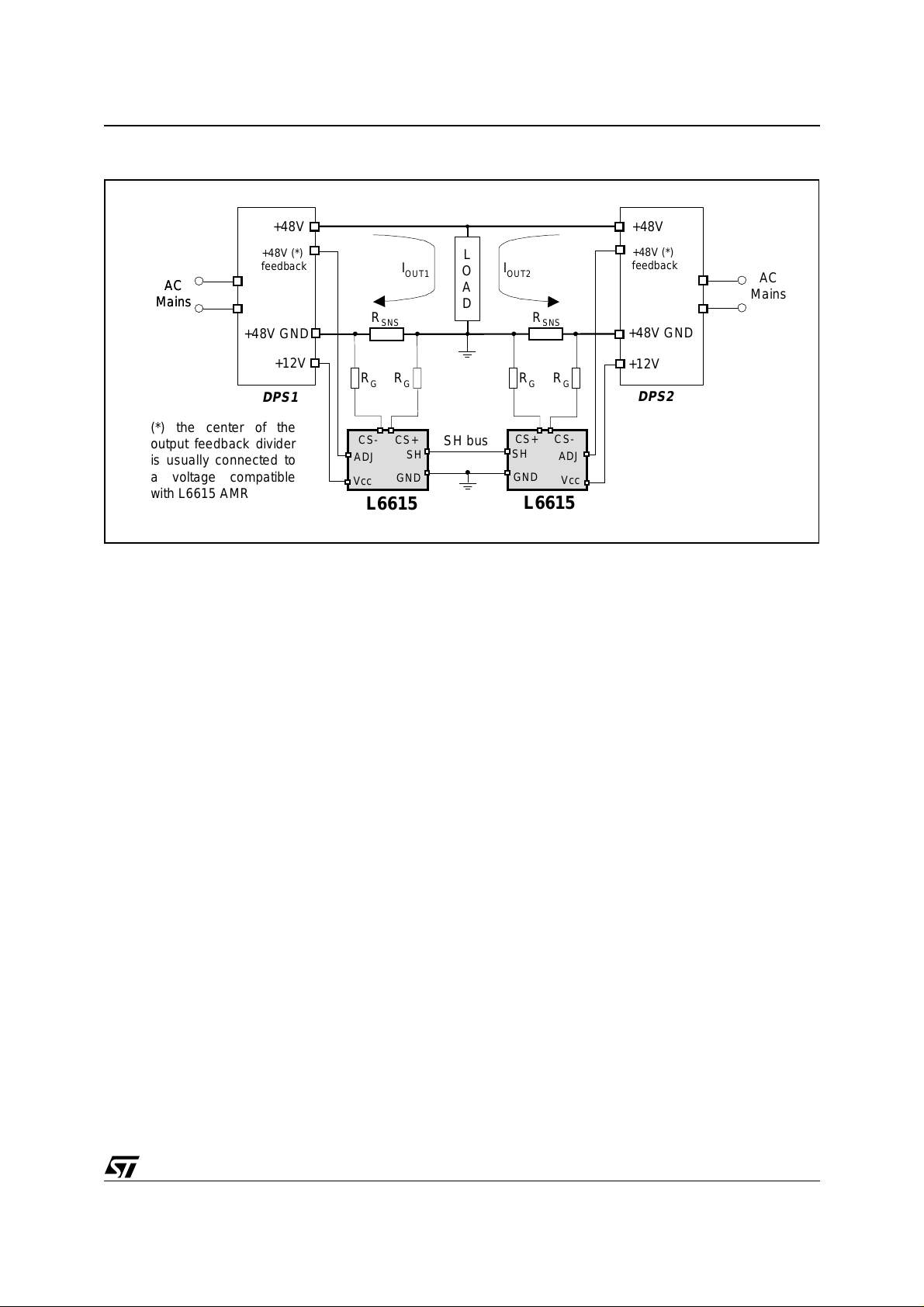
Figure 15. Distributed power system for +48V bus
000000000000000000000000000
0
00000
0
00000
0
00000
0
00000
0
00000
0
00000
0
00000
0
00000
0
00000
000000000000000000000000000
00000
00000
00000
00000
00000
00000
00000
00000
00000
L6615
000000000000000000000
+48V
000000000000000000000
000000000000000000000
+48V (*)
000000000000000000000
feedback
AC
AC
Mains
Mains
000000000000000000000
000000000000000000000
000000000000000000000
+48V GND
000000000000000000000
000000000000000000000
+12V
DPS1
(*) the center of the
output feedback divider
is usually connected to
a voltage compatible
with L6615 AMR
R
SNS
R
GRG
CS- CS+
ADJ
Vcc
L6615
I
OUT1
SH
GND
L
O
A
D
SH bus
I
OUT2
R
SH
GND
R
SNS
GRG
CS-CS+
ADJ
Vcc
L6615
00000000000000000000000
+48V
00000000000000000000000
00000000000000000000000
+48V (*)
00000000000000000000000
feedback
00000000000000000000000
00000000000000000000000
AC
Mains
00000000000000000000000
+48V GND
00000000000000000000000
00000000000000000000000
+12V
DPS2
In this application is inserted also a circuit for the square current limit protection in case of overcurrent (R1Q1): being the vo ltage a t the CGA pin directly proportional to t he cu rrent carried by the relevan t section,
it is possible to set the CGA resistor such that, until the output current is in the right range, the CGA voltage
is lower than V
+0.7. As soon as this value is overcome, then the bipolar pushes current in the feedback
REF
path, reducing the duty cycle and consequently the output voltage.
Current sharing can be required in AC to DC application like distributed power system (DPS) for telecom
applications: if the output voltage is hi gher than the absol ute maximum rating for the current sense pins
(CS+ and CS-) high side sens ing can not be performed unless adding other c omponents; the current
sense is performed on the ground return.
To maintain high side sensing t wo resistor d ividers (between the edge of R
and ground) could be
SENSE
introduced to translate the sense signal in the L6615 input pin common mode range.
In fig.15 two AC-DC converters supply the same load through a +48V bus; these converters usually exhibit
also a +12V auxiliary output useful to supply the L6615 whose ADJ pin works on the +48V feedback section (COMP pin and CGA pin connections are not showed) in figure 15.
7 LOW VOLTAGE BUSES
The L6615 has a "doubled" sense structure, designed to perform both high side and low side sensing: the
first solution is usually conside red m ore convenient. Actually low side se nsing mea ns t o spl it t he g round
return as many times as the power supplies paralleled are: on each of these paths it is then necessary to
place the sense resistor introducing a drop between the power supply ground and the common load negative reference.
The voltage at CS+ pi n is read by an internal comparat or a nd c om pared with a reference corresponding
to the switchover threshold V
whose value is typically 1.6V. If such value is overcome, then the com-
THcs+
parator triggers the High Side Amplifier (HSA); bein g t he thres hol d provided by hysteresis, then t he Low
Side Amplifier (LSA) will be triggered as VCS+ is lower than 1.44V (typ.).
Hence V
defines the threshold between the operating range of LSA, (referring to fig.10) and the op-
THcs+
erating range of HSA; usually LSA is operating when the sense resistor is placed on the ground return,
between the negative load terminal and the negative powe r supply output (fig 10.b) and HSA when the
sense resistor is placed between the power supply positive output and the load.
It is however possible to perform high side sensing for applications whose output voltage is close to V
threshold (or even lower) exploiting the low sense internal structure (LSA).
THcs+
15/20
L6615
Consider, for example an application with V
= 1.2V and the sense resistor placed high side; the voltage
OUT
at CS+:
V
CS+
= V
OUT
- ∆V
SENSE
is lower than 1.6V so the internal comparator triggers on the LSA structure and the pin CS- sources the
curre nt I
(see paragraph "2. CURRENT SEN SE SECTION"). The IC works properly bec ause the dy-
CS
namics of LSA spreads down to zero: in this case it is necessary to pay at tention to the design of ADJ
network.
Now consider, for example, an application with V
=1.5V where, because of the drop across R
OUT
SNS
, the
voltage at CS+ pin could be very close to the t hreshold : if such v oltage i s overco me (start-up, loa d regulation, overvoltage,…) , then the HSA structure will be activated; as nominal conditions are rest ored, t he
hysteresis will then keep HSA acti ve (unles s V
falls under the lower threshold).
CS+
8 OFFSE T TR IMMING
The current sharing accuracy strongly depends on the unbalance between the relevant parameters of the
paralleled sections. Ea ch perc entage point on the rel ev ant param eters tolerance introduces a maxi mum
error equal to the double of the tolerance.The L6615 introduces an inherent error in current sharing due
to the 40mV offset at the negative input of the error amplifier; this offset is necessary to guarantee the low
value of the master COMP pin.
Considering perfectly matched all other parameters, the offset introduces a percentage error equal to 4%
divided by the voltage on the share bus. In particular:
40mA
1
--------------- -–
⋅=
V
SH
CGA/RG
, higher are the currents
Being V
I
SLAVEIMASTER
directly proportional to the load current and f ixed the ratio R
SH
involved in the sharing, lower is the error.
Another error is introduced by the current sense amplifier due to its in put offset whose amplitude can be
±1mV: being typically the drop across R
about one hundred mV at full load, the offset could lead to an
SNS
error of some percentage point.
Whenever the application requires very high current sharing accuracy, it is possible to correct these offsets
through a triggering process, introducing a trimmer (R
) between current sense input pins.
K
Referring to fig. 16, in case of high side sensing, the equations governing the circuit are:
V
–
OUTVM
---------------------------- -
R
G
V
M
---------------------------- -=
1 δ–()R
⋅
K
V
OUTVSENSEVP
-------------------------------------------------------- -
R
VP = VM + V
–+
G
O
V
P
-------------- -– I
δ RK⋅
=
G
where VO is the current sense amplifier input offset.
Solving fo r I
Ideally I
, we get:
G
+⋅
G
δ R
KRG
----------------------------- -
⋅⋅
δ R
KRG
V
OVOUT
⋅+⋅–=
δ R
1 δ–()R
K
+⋅[]⋅
2 δ 1–⋅
--------------------------------------------------------
G
V
G
SENSE
--------------------- -
R
I
should be equal only to the first term: this current will be sunk by CS+ pin, internally mirrored
G
with 1:1 ratio and sent to CGA pin.
Imposing that the sum of two latter terms is zero it is possible to find the value of δ deleting the ef fect of
the offset:
16/20
δ
OPT
1
-- -
2
2V
----------------------------------------------------------------------------------------------------------------------------------------------------------- -–=
OUTRG
4V
2
OUT
2
R
G
⋅⋅
2V
ORK
2
2
V
R
O
K
4V
⋅⋅⋅+⋅+⋅⋅–⋅⋅
2
O
RGR
K
Figure 16. Offset Trimming
V
V
OUT+VSENSE
OUT+VSENSE
L6615
I
I
LOAD
LOAD
_
+
+
R
R
G
G
_
R
R
SNS
SNS
V
V
OUT
OUT
R
R
G
G
δ R
δ R
I
I
G
G
V
V
P
P
CS+
CS+
CGA
CGA
R
R
CGA
CGA
K
K
L6615
L6615
(1-δ) R
(1-δ) R
K
K
V
V
M
M
CS-
CS-
Because of the tolerance of the output voltage, it is not possible to delete completely the effect of the offset
on CGA pin on all the allowed output voltage range: if the trimming operation is performed at V
then on pin CGA the maximum residual voltage will be present at V
⋅⋅
R
CGAVOUT MAX()
V
–()
OUT MI N()
---------------------------------------------------------------------------- -
δ
OPTRKδOPTRK
12δ
OUT(MAX)
and its value will be:
⋅–
OPT
– RG–⋅()⋅
OUT(MIN)
To simplify the procedure, the following step-by step process can be used:
■ a trimmer has to be placed between sense pins of each section: the value of the trimmer resistance
must be at least one order of magnitude higher than R
and it has to be set at one half of its range
G
(δ=0.5);
■ once the application is running at a load defined by the designer based on the required sharing
accuracy, the master section has to be located;
■ on the slave sections it is then necessary to operate on the trimmer to make equal the output currents.
REFERENCE
,
[1] "L6910 - Adjustable step down controller with synchronous rectification" (Datasheet)
[2] "L6911 - 5 bit programmable step down controller with synchronous rectification" (Datasheet
17/20
L6615
mm inch
DIM.
MIN. TYP. MAX. MIN. TYP. MAX.
A 3.32 0.131
a1 0.51 0.020
B 1.15 1.65 0.045 0.065
b 0.356 0.55 0.014 0.022
b1 0.204 0.304 0.008 0.012
D 10.92 0.430
E 7.95 9.75 0.313 0.384
e2.54 0.100
e3 7.62 0.300
e4 7.62 0.300
F 6.6 0.260
OUTLINE AND
MECHANICAL DATA
I 5.08 0.200
L 3.18 3.81 0.125 0.150
Z 1.52 0.060
Minidip
18/20

L6615
DIM.
D (1) 4.8 5.0 0.189 0.197
F (1) 3.8 4.0 0.15 0.157
(1) D and F do not include mold flash or protrusions. Mold flash or
potrusions shall not exceed 0.15mm (.006inch).
MIN. TYP. MAX. MIN. TYP. MAX.
A 1.75 0.069
a1 0.1 0.25 0.004 0.010
a2 1.65 0.065
a3 0.65 0.85 0.026 0.033
b 0.35 0.48 0.014 0.019
b1 0.19 0.25 0.007 0.010
C 0.25 0.5 0.010 0.020
c1 45° (typ.)
E 5.8 6.2 0.228 0.244
e 1.27 0.050
e3 3.81 0.150
L 0.4 1.27 0.016 0.050
M 0.6 0.024
S8° (max.)
mm inch
OUTLINE AND
MECHANICAL DATA
SO8
19/20

L6615
Information furnished is believed to be accurate and reliable. However, STMicroelectronics assumes no responsibility for the consequences
of use of such information nor for any infringement of patents or other rights of third parties which may result from its use. No license is granted
by implic ation or oth erwise unde r any paten t or patent ri ghts of STMi croelectronics. Spec i fications me ntioned in this publication are s ubj ect
to change without notice. This publication supersedes and replaces all information previously supplied. STMicroelectronics product s are not
authorized for use as critical components in life su pport device s or systems without express written approval of STMicroelectronics.
The ST logo is a registered trademark of STMicroelectronics
2003 STMicroelectr oni cs - All Rights Reserved
Austra lia - Brazil - Canada - China - F i nl and - France - Germany - Hong Kong - India - Israel - Ital y - J apan -Malay sia - Malta - Morocco -
Singap ore - Spain - Sw eden - Switzerl and - United K i ngdom - United States.
STMicroelectronics GROUP OF COMPANIES
http://www.s t. com
20/20
 Loading...