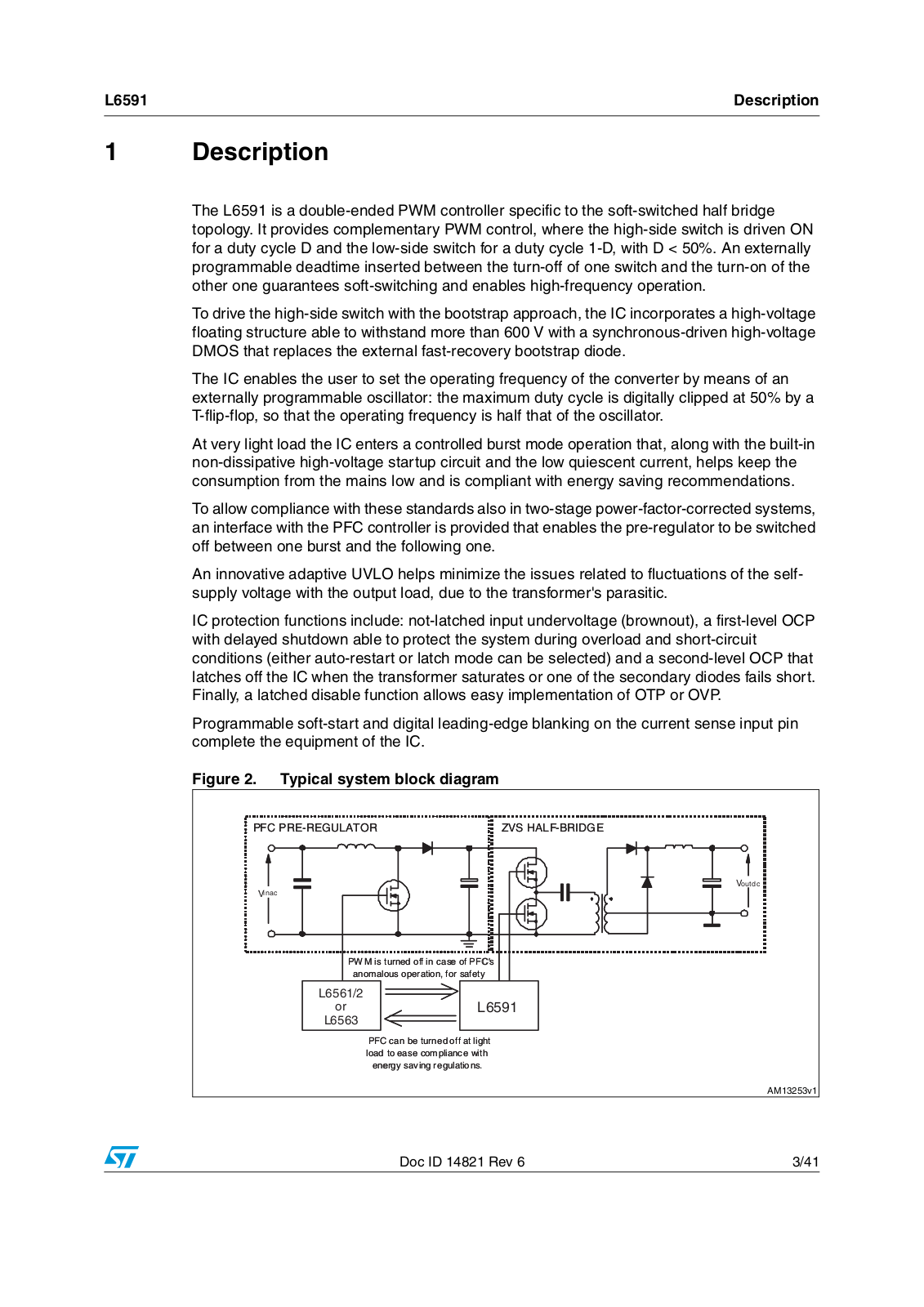
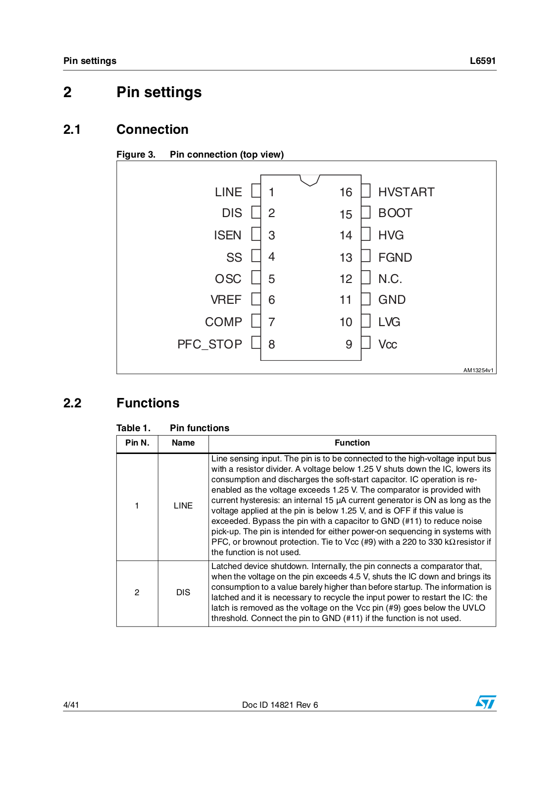
ST L6591 User Manual

L6591

PWM controller for ZVS half bridge

Features

Complementary PWM control for soft-switched half bridge with programmable deadtime

Up to 500 kHz operating frequency

Onboard high-voltage startup

Advanced light load management

Adaptive UVLO

Pulse-by-pulse OCP

OLP (latched or autorestart)

Transformer saturation detection

Interface with PFC controller

Latched disable input

Input for power-on sequencing or brownout protection

Programmable soft-start

Figure 1. Block diagram

Datasheet production data

SO16 narrow

4% precision external reference

600 V-rail compatible high-side gate driver with integrated bootstrap diode and high dV/dt immunity

SO16N package

Applications

High power AC-DC adapter/charger

Desktop PC, entry-level server

Telecom SMPS


HV

VCC


16

9


5

CLK


OSC


TIMING

25 V


Vref


HV generator ON/O FFa nd

VREG


a daptive UV LOmanagement


Vcc_OK


2


R

Low


DIS

+


UVLO


S

Q


4.5V

-


DIS


1.5V

HICCUP


-


BLANKI NG

S

Q

P WM _CT L


ISEN

+


R


tment


3


+


8


S

PWM

LI NE_ OK


timedadjus

&logic


OCP2

Vc c_O K


R

-

DIS

S HUT DO WN


PFC_STOP


Q


Dea


OCP2


BURST- M ODE CTRL


VREG


DI S


Ilimref


+


0.32mA


+


0.8 V max.


1.25V

OCP


-


LI NE_OK

-


1

-


1.75V


-


LINE

+


3R


15µA


SOFT-START

R


+


2.0V


4


7


SS


COMP


6


VREF


Sync hronou s


bootstra p diode


15


BOOT

LEVEL

14

HVG

SHIFTER


13


FGND

V CC

10

LV G

Low

11

UV LO

GND

August 2012

Doc ID 14821 Rev 6

1/41

This is information on a product in full production.

www.st.com

Contents

L6591


Contents

1

Description . . . . . . . . . . . . . . . . . . . . . . . . . . . . . . . . . . . . . . . . . . . . . . . .

. 3

2

Pin settings . . . . . . . . . . . . . . . . . . . . . . . . . . . . . . . . . . . . . . . . . . . . . . .

. 4


2.1

Connection . . . . . . . . . . . . . . . . . . . . . . . . . . . . . . . . . . . . . . . . . . . . . . . . .

4


2.2

Functions . . . . . . . . . . . . . . . . . . . . . . . . . . . . . . . . . . . . . . . . . . . . . . . . . .

4

3

Electrical data . . . . . . . . . . . . . . . . . . . . . . . . . . . . . . . . . . . . . . . . . . . . . .

7


3.1

Maximum ratings . . . . . . . . . . . . . . . . . . . . . . . . . . . . . . . . . . . . . . . . . . . .

7


3.2

Thermal data . . . . . . . . . . . . . . . . . . . . . . . . . . . . . . . . . . . . . . . . . . . . . . .

7

4

Electrical characteristics . . . . . . . . . . . . . . . . . . . . . . . . . . . . . . . . . . . . .

8

5

Typical characteristics . . . . . . . . . . . . . . . . . . . . . . . . . . . . . . . . . . . . . .

12

6

Application information . . . . . . . . . . . . . . . . . . . . . . . . . . . . . . . . . . . . .

21

6.1 High-voltage startup generator . . . . . . . . . . . . . . . . . . . . . . . . . . . . . . . . . 22 6.2 Operation at no load or very light load . . . . . . . . . . . . . . . . . . . . . . . . . . . 24 6.3 PWM control block . . . . . . . . . . . . . . . . . . . . . . . . . . . . . . . . . . . . . . . . . . 26 6.4 PWM comparator, PWM latch and hiccup mode OCP . . . . . . . . . . . . . . . 26 6.5 Latched shutdown . . . . . . . . . . . . . . . . . . . . . . . . . . . . . . . . . . . . . . . . . . 27 6.6 Oscillator and deadtime programming . . . . . . . . . . . . . . . . . . . . . . . . . . . 28 6.7 Adaptive UVLO . . . . . . . . . . . . . . . . . . . . . . . . . . . . . . . . . . . . . . . . . . . . . 30 6.8 Line sensing function . . . . . . . . . . . . . . . . . . . . . . . . . . . . . . . . . . . . . . . . 31 6.9 Soft-start and delayed latched shutdown upon overcurrent . . . . . . . . . . . 32

7

Summary of L6591 power management functions . . . . . . . . . . . . . . .

34

8

ECOPACK® . . . . . . . . . . . . . . . . . . . . . . . . . . . . . . . . . . . . . . . . . . . . . . . . . . . . . . . . . . . .

. 37

9

Order codes . . . . . . . . . . . . . . . . . . . . . . . . . . . . . . . . . . . . . . . . . . . . . . .

39

10

Revision history . . . . . . . . . . . . . . . . . . . . . . . . . . . . . . . . . . . . . . . . . . .

40

2/41

Doc ID 14821 Rev 6

L6591

Description


1 Description

The L6591 is a double-ended PWM controller specific to the soft-switched half bridge topology. It provides complementary PWM control, where the high-side switch is driven ON for a duty cycle D and the low-side switch for a duty cycle 1-D, with D < 50%. An externally programmable deadtime inserted between the turn-off of one switch and the turn-on of the other one guarantees soft-switching and enables high-frequency operation.

To drive the high-side switch with the bootstrap approach, the IC incorporates a high-voltage floating structure able to withstand more than 600 V with a synchronous-driven high-voltage DMOS that replaces the external fast-recovery bootstrap diode.

The IC enables the user to set the operating frequency of the converter by means of an externally programmable oscillator: the maximum duty cycle is digitally clipped at 50% by a T-flip-flop, so that the operating frequency is half that of the oscillator.

At very light load the IC enters a controlled burst mode operation that, along with the built-in non-dissipative high-voltage startup circuit and the low quiescent current, helps keep the consumption from the mains low and is compliant with energy saving recommendations.

To allow compliance with these standards also in two-stage power-factor-corrected systems, an interface with the PFC controller is provided that enables the pre-regulator to be switched off between one burst and the following one.

An innovative adaptive UVLO helps minimize the issues related to fluctuations of the selfsupply voltage with the output load, due to the transformer's parasitic.

IC protection functions include: not-latched input undervoltage (brownout), a first-level OCP with delayed shutdown able to protect the system during overload and short-circuit conditions (either auto-restart or latch mode can be selected) and a second-level OCP that latches off the IC when the transformer saturates or one of the secondary diodes fails short. Finally, a latched disable function allows easy implementation of OTP or OVP.

Programmable soft-start and digital leading-edge blanking on the current sense input pin complete the equipment of the IC.

Figure 2. Typical system block diagram

PFC PRE-REGULATOR

ZVS HALF-BRIDGE

Voutd c

Vinac

PW M is turned off in case of PFC's anomalous operation, for safety

L6561/2

or L6591

L6563

PFC can be turned off at light load to ease compliance with energy saving regulations.

AM13253v1

Doc ID 14821 Rev 6

3/41

Pin settings

L6591


2 Pin settings

2.1Connection

Figure 3. Pin connection (top view)

LINE


1

16


HVSTART


DIS


2

15


BOOT


ISEN


3

14


HVG


SS


4

13


FGND


OSC


5

12


N.C.


VREF


6

11


GND


COMP


7

10


LVG


PFC_STOP


8

9


Vcc


AM13254v1

2.2Functions

Table 1.

Pin functions

Pin N.

Name

Function


Line sensing input. The pin is to be connected to the high-voltage input bus


with a resistor divider. A voltage below 1.25 V shuts down the IC, lowers its


consumption and discharges the soft-start capacitor. IC operation is re-


enabled as the voltage exceeds 1.25 V. The comparator is provided with

1

LINE

current hysteresis: an internal 15 µA current generator is ON as long as the

voltage applied at the pin is below 1.25 V, and is OFF if this value is


exceeded. Bypass the pin with a capacitor to GND (#11) to reduce noise


pick-up. The pin is intended for either power-on sequencing in systems with


PFC, or brownout protection. Tie to Vcc (#9) with a 220 to 330 kΩ resistor if


the function is not used.


Latched device shutdown. Internally, the pin connects a comparator that,


when the voltage on the pin exceeds 4.5 V, shuts the IC down and brings its

2

DIS

consumption to a value barely higher than before startup. The information is

latched and it is necessary to recycle the input power to restart the IC: the


latch is removed as the voltage on the Vcc pin (#9) goes below the UVLO


threshold. Connect the pin to GND (#11) if the function is not used.


4/41

Doc ID 14821 Rev 6

L6591


Pin settings


Table 1.

Pin functions (continued)


Pin N.

Name

Function


Current sense (PWM comparator) input. The voltage on this pin is internally


compared with an internal reference derived from the voltage on the COMP


pin and, when they are equal, the high-side gate drive output (previously


asserted high by the clock signal generated by the oscillator) is driven low to


turn off the upper Power MOSFET; the lower MOSFET is turned on after a


delay programmed by the timing capacitor at the OSC pin (#5). The pin is


3

ISEN

equipped with 200 ns blanking time for improved noise immunity. A second


comparator, referenced at 0.8 V, turns off the upper MOSFET if the voltage


at the pin exceeds the threshold, overriding the PWM comparator (pulse-by-


pulse OCP). A third comparison level located at 1.5 V shuts the device


down and brings its consumption almost to a “before startup” level (hiccup


mode OCP) to prevent uncontrolled current rise. A logic circuit improves


sensitivity to temporary disturbances.


Soft-start. An internal 20 µA generator charges an external capacitor


connected between the pin and GND (#11) generating a voltage ramp.


During the ramp, the internal reference for pulse-by-pulse OCP (see pin #3,


ISEN) rises linearly starting from zero to its final value, therefore causing


4

SS

the duty cycle of the upper MOSFET to rise starting from zero as well, and


all the functions monitoring the COMP pin (#7) are disabled. The same


capacitor is used to delay IC shutdown (latch-off or auto-restart mode


selectable) after detecting an overcurrent condition. The SS capacitor is


quickly discharged as the chip goes into UVLO.


Oscillator pin. A resistor to VREF (#6) and a capacitor from the pin to GND


(#11) define the oscillator frequency. The maximum duty cycle is limited


5

OSC

below 50% by an internal T-flip-flop. As a result, the switching frequency is


half that of the oscillator. The capacitor value defines the deadtime


separating the conduction state of either MOSFET. This capacitor should


not be lower than 220 pF.


Voltage reference. An internal generator furnishes an accurate voltage


reference (5 V±4%, all inclusive) that can be used to supply up to 5 mA to


6

VREF

an external circuit. A small film capacitor (0.1 µF typ.), connected between


this pin and GND (#11) is recommended to ensure the stability of the


generator and to prevent noise from affecting the reference.


Control input for PWM regulation. The pin is to be driven by the


phototransistor (emitter-grounded) of an octocoupler to modulate the


voltage by modulating the current sunk from (sourced by) the pin (0.4 mA


typ.). It is recommended to place a small filter capacitor between the pin


7

COMP

and GND (#11), as close to the IC as possible, to reduce switching noise


pick-up, and to set a pole in the output-to-control transfer function. A voltage


lower than 1.75 V shuts down the IC and reduces its current consumption.


The chip restarts as the voltage exceeds 1.8 V. This function realizes burst


mode operation at light load.


Open-drain ON/OFF control of PFC controller. This pin is intended for


temporarily stopping the PFC controller at light load in systems comprising


a PFC pre-regulator, during burst mode operation (see pin COMP, #7). The


8

PFC_STOP

pin, normally open, goes low if the voltage on COMP is lower than 1.75 V


and opens when the voltage on the COMP pin exceeds 1.8 V. Whenever the


IC is shut down (SS > 5 V, DIS > 4.5, ISEN > 1.5 V) the pin is low as well,


provided the supply voltage of the IC is above the restart threshold


(typ. 5 V). It is open during UVLO. Leave the pin open if not used.


Doc ID 14821 Rev 6

5/41

Pin settings


L6591


Table 1.

Pin functions (continued)


Pin N.

Name

Function


Supply voltage of both the signal part of the IC and the low-side gate driver.


The internal high-voltage generator charges an electrolytic capacitor


connected between this pin and GND (#11) as long as the voltage on the


pin is below the startup threshold of the IC, after that, it is disabled and the


9

Vcc

chip turns on. Sometimes a small bypass capacitor (0.1 µF typ.) to GND


may be useful to get a clean bias voltage for the signal part of the IC. The


minimum operating voltage (UVLO) is adapted to the loading conditions of


the converter to ease burst mode operation, during which the available


supply voltage for the IC drops.


Low-side gate-drive output. The driver is capable of 0.3 A min. source and


10

LVG

0.8 A min. sink peak current to drive the gate of the lower MOSFET of the


half bridge leg. The pin is actively pulled to GND (#11) during UVLO.


Chip ground. Current return for both the low-side gate-drive current and the


11

GND

bias current of the IC. All of the ground connections of the bias components


should be tied to a track going to this pin and kept separate from any pulsed


current return.


High-voltage spacer. The pin is not connected internally to isolate the group


12

N.C.

of high-voltage pins and comply with safety regulations (creepage distance)


on the PCB.


High-side gate-drive floating ground. Current return for the high-side gate-


13

FGND

drive current. Layout carefully the connection of this pin to avoid too large


spikes below ground.


High-side floating gate-drive output. The driver is capable of 0.3 A min.


14

HVG

source and 0.8 A min. sink peak current to drive the gate of the upper


MOSFET of the half bridge leg. A pull-down resistor between this pin and


pin 13 (FGND) makes sure that the gate is never floating during UVLO.


High-side gate-drive floating supply voltage. The bootstrap capacitor


15

BOOT

connected between this pin and pin 13 (FGND) is fed by an internal


synchronous bootstrap diode driven in-phase with the low-side gate-drive.


This patented structure can replace the normally used external diode.


High-voltage startup. The pin is to be connected directly to the rectified


mains voltage. A 0.8 mA internal current source charges the capacitor


connected between pin Vcc (#9) and GND (#11) until the voltage on the Vcc


16

HVSTART

pin reaches the startup threshold. Normally it is re-enabled when the


voltage on the Vcc pin falls below 5 V, except under latched shutdown


conditions, in which case it is re-enabled as the Vcc voltage falls 1 V below


the startup threshold to keep the latch active.


6/41

Doc ID 14821 Rev 6

L6591

Electrical data


3 Electrical data

3.1Maximum ratings

Table 2.

Absolute maximum ratings


Symbol

Pin

Parameter

Value

Unit


VHVSTART

16

Voltage range (referred to ground)

-0.3 to 700

V

IHVS

16

Input current

Self-limited

A

VBOOT

15

Floating supply voltage

-1 to 618

V

VFGND

13

Floating ground voltage

-3 to VBOOT -18

V

dVFGND/dt

13

Floating ground slew rate

50

V/ns

VCC

9

IC supply voltage (Icc = 20 mA)

Self-limited

V

IHVG, ILVG

10, 14

Gate drive peak current

Self-limited

A

IPFC_STOP

8

Max. sink current (VPFC_STOP = 25 V)

Self-limited

A

VLINEmax

1

Maximum pin voltage (Ipin 1 mA)

Self-limited

V

-

2 to 7

Analog inputs and outputs

-0.3 to 7

V


ISEN

3

Current sense input

-3 to 7

V


PTOT


Power dissipation @ TA = 50 °C

0.75

W

TJ


Junction temperature operating range

-40 to 150

°C

TSTG


Storage temperature

-55 to 150

°C

3.2Thermal data

Table 3.

Thermal data


Symbol

Parameter

Value

Unit


R

Thermal resistance junction-to-ambient (1)

120

°C/W

thJA


1. Value depending on PCB copper area and thickness.

Doc ID 14821 Rev 6

7/41

Electrical characteristics

L6591


4 Electrical characteristics

TJ = 0 to 105 °C, Vcc = 15 V, VBOOT = 12 V, CHVG = CLVG = 1 nF; RT = 22 kΩ, CT = 330 pF; unless otherwise specified.

Table 4.

Electrical characteristics


Symbol

Parameter

Test condition

Min.

Typ.

Max.

Unit


IC supply voltage


Vcc

Operating range after

VCOMP > VCOMPL

11.3


22

V

turn-on

VCOMP = VCOMPL

9.2


22


VccOn

Turn-on threshold

(1)


13

14

15

V


VccOff

Turn-off threshold

(1) VCOMP > VCOMPL

9.7

10.5

11.3

V

(1) V

COMP

= V

8.2

8.7

9.2


COMPL


Hys

Hysteresis

VCOMP > VCOMPL

3.0

3.5


V

VZ

Vcc clamp voltage

Icc = 15 mA

22

25

28

V

Supply current


Istartup

Startup current

Before turn-on,


190

250

µA

Vcc = 12.5 V


Iq

Quiescent current

After turn-on


2.8

3.5

mA


Icc

Operating supply current


5.3

8

mA


VDIS > 4.5 V,


0.35

mA

Iqdis

Shutdown quiescent

VISEN > 1.5 V


current

VCOMP = 1.64 V


2.2

mA


VLINE < 1.25 V


0.35

mA

High-side floating gate-drive supply


VBOOT

Operating supply voltage

Referred to FGND pin


17

V

IqBOOT

Quiescent current

VFGND = 0


500

800

µA

ILK

High-voltage leakage

VFGND = VBOOT =


10

µA

VHVG = 600 V


RDS(on)

Synchronous bootstrap

VLVG = HIGH


125


diode on-resistance


High-voltage startup generator


VHV

Breakdown voltage

IHV < 100 µA

700


V

VHVstart

Start voltage

IVcc < 100 µA

60

75

90

V

Icharge

Vcc charge current

VHV > VHvstart,

0.55

0.75

1

mA

Vcc > 3 V


8/41

Doc ID 14821 Rev 6

L6591


Electrical characteristics


Table 4.

Electrical characteristics (continued)


Symbol

Parameter

Test condition

Min.

Typ.

Max.

Unit


VHV > VHvstart,


1.6


IHV, ON

ON-state current

Vcc > 3 V


mA


VHV > VHvstart, Vcc = 0


0.8


IHV, OFF

Leakage current (OFF-state)

VHV = 400 V


40

µA


VCCrestart

HV generator restart voltage

(1)

4.4

5

5.6

V


(1) After DIS tripping

12.2

13.2

14.2

V


Reference voltage


VREF

Output voltage

(1) TJ = 25 °C;

4.9

5

5.1

V


IREF = 1 mA


VREF

Total variation

Vcc= 9.2 to 22 V,

4.8


5.2

V


IREF = 1 to 5 mA


IREF

Short-circuit current

VREF = 0

10


30

mA


Sink capability in UVLO

Vcc = 6 V;


0.2

0.5

V


Isink = 0.5 mA


Current sense comparator


IISEN

Input bias current

VISEN = 0


-1

µA


tLEB

Leading edge blanking

After VHVG low-to-high


200


ns


transition


td(H-L)

Delay to output


170

ns


Gain


3.8

4

4.2

V/V


VISENx

Maximum signal

(1) VCOMP = 5 V

0.76

0.8

0.84

V


VISENdis

Hiccup mode OCP level

(1)

1.4

1.5

1.65

V


PWM control and burst mode control


VCOMPH

Maximum level

ICOMP = 0

5.5


V


ICOMP

Source current

VCOMP = 2 V

210

300

400

µA


RCOMP

Dynamic resistance

VCOMP = 2 to 4 V


25


kΩ


VCOMPBon

Burst mode on threshold

(1) VCOMP falling

1.68

1.75

1.82

V


Hys

Burst mode hysteresis

VCOMP rising


70


mV


Dmax

Maximum duty cycle

VCOMP = 5 V

46


50

%


Adaptive UVLO


VCOMPL

UVLO shift threshold

(1)

1.9

2

2.1

V


Line sensing


Vth

Threshold voltage

Voltage rising or falling

1.22

1.25

1.28

V


IHys

Current hysteresis

Vcc > 5 V

13.2

14.7

16.2

µA


Vclamp

Clamp level

ILINE = 1 mA

2.8

3


V

Doc ID 14821 Rev 6

9/41

Electrical characteristics


L6591


Table 4.

Electrical characteristics (continued)


Symbol

Parameter

Test condition

Min.

Typ.

Max.

Unit


DIS function


IOTP

Input bias current

VDIS = 0 to Vth


-1

µA


Vth

Disable threshold


4.275

4.5

4.725

V


Oscillator and deadtime programming


fosc

Oscillation frequency

TJ = 25 °C

170

180

190

kHz


Vcc = 9.2 to 22 V

168

180

192

kHz


Vpk

Oscillator peak voltage

(1)

2.85

3

3.15

V


Vvy

Oscillator valley voltage

(1)

0.75

0.9

1.05

V


Deadtime


0.42


(VHVG high-to-low to VLVG


CT = 1 nF


1.0


Tdead

low-to-high transition)


µs


Deadtime (VLVG high-to-low


0.42


to VHVG low-to-high


CT = 1 nF


1.0


transition)


Soft-start


TJ = 25 °C, VSS < 1.5 V,

14

18

22


ISSC

Charge current

VCOMP = 4 V


µA


TJ = 25 °C, VSS > 1.5 V,

3.4

4.7

5.6


VCOMP = VCOMPH


ISsdis

Discharge current

VSS > 1.5 V

3.4

4.7

5.6

µA


VSsclamp

High saturation voltage

VCOMP = 4 V


2


V


VSSDIS

Disable level

(2) VCOMP = VCOMPH

4.85

5

5.15

V


VSSLAT

Latch-off level

VCOMP = VCOMPH


6.4


V


PFC_STOP function


Ileak

High level leakage current

VPFC_STOP = Vcc,


1

µA


VCOMP = 2 V


VL

Low saturation level

IPFC_STOP = 2 mA


0.1

V


VCOMP = 1.5 V


Low-side gate driver (voltages referred to GND)


VLVGL

Output low-voltage

Isink = 200 mA


1.0

V


VLVGH

Output high-voltage

Isource = 5 mA

12.8

13.3


V


Isourcepk

Peak source current (2)


-0.3


A


I

Peak sink current (2)


0.8


A


sinkpk


10/41

Doc ID 14821 Rev 6

L6591


Electrical characteristics


Table 4.

Electrical characteristics (continued)


Symbol

Parameter

Test condition

Min.

Typ.

Max.

Unit


tf

Fall time


40


ns


tr

Rise time


80


ns


UVLO saturation

Vcc = 0 to VccOn,


1.1

V


Isink = 1 mA


High-side gate driver (voltages referred to FGND)


VHVGL

Output low-voltage

Isink = 200 mA


1.5

V


VHVGH

Output high-voltage

Isource = 5 mA

11

11.9


V


Isourcepk

Peak source current (2)


-0.3


A


I

Peak sink current (2)


0.8


A


sinkpk


tf

Fall time


40


ns


tr

Rise time


80


ns


Pull-down resistor


25


kΩ


1.Parameters tracking each other.

2.Parameters guaranteed by design.

Doc ID 14821 Rev 6

11/41

Typical characteristics

L6591


5 Typical characteristics

Figure 4. High-voltage generator ON-state

Figure 5. High-voltage generator output

sink current vs. Tj

(Vcc charge current) vs. Tj


ϭ͘Ϯ


ϭϭϬй


ϭ


ϭϬϱй


sĐĐш ϯs


Ϭ͘ϴ


ϭϬϬй


sĐĐ ш ϯs


й


ŵ/,s


sĐĐ с Ϭs


Ϭ͘ϲ


Z',

ϵϱй


/


Ϭ͘ϰ


ϵϬй


Ϭ͘Ϯ


ϴϱй


Ϭ


ϴϬй


ϱϬ

Ϭ

ϱϬ

ϭϬϬ

ϭϱϬ


ϱϬ

Ϭ

ϱϬ

ϭϬϬ

ϭϱϬ


dũ Σ


dũ Σ


". W


". W

Figure 6. High-voltage generator start

Figure 7. High-voltage generator Vcc restart

voltage vs. Tj

voltage vs. Tj

ϭϭϬй


ϭϰ


ϭϮ


ϭϬϱй


ϭϬ


s


ĂĨƚĞƌ /^ƚƌŝƉƉŝŶŐ


ϴ


ŶŽƌŵĂů ŽƉĞƌĂƚŝŽŶ


ϭϬϬй


ƌĞƐƚĂƌƚ


s,sƐƚĂƌƚй


ϲ


s


ϵϱй


ϰ


Ϯ


ϵϬй


Ϭ


ϱϬ

Ϭ

ϱϬ

ϭϬϬ

ϭϱϬ


ϱϬ

Ϭ

ϱϬ

ϭϬϬ

ϭϱϬ


dũ Σ


dũ Σ


". W


". W

12/41

Doc ID 14821 Rev 6

ST L6591 User Manual

L6591

Typical characteristics


Figure 8. IC consumption during normal

Figure 9. IC consumption under protection

operation vs. Tj

and before turn-on vs. Tj


ϲ


Ϭ͘ϯϱ


ϱ


Ϭ͘ϯ


KƉĞƌĂƚŝŶŐ


Ϭ͘Ϯϱ


ϰ


YƵŝĞƐĐĞŶƚ


ƵƌƐƚŵŽĚĞ


/ĐĐ ŵ

Ϭ͘Ϯ


/ĐĐ ŵ


ϯ


Ϭ͘ϭϱ


Ϯ


>/E ф ϭ͘ϰϰs


Ϭ͘ϭ


/^ хϰ͘ϱs


/^ E хϭ͘ϱs


ϭ


Ϭ͘Ϭϱ


ĞĨŽƌĞƚƵƌŶŽŶ ;sĐĐсϭϮ͘ϱs


Ϭ


Ϭ


ϱϬ

Ϭ

ϱϬ

ϭϬϬ

ϭϱϬ


ϱϬ

Ϭ

ϱϬ

ϭϬϬ

ϭϱϬ


dũ Σ


dũ Σ


". W


". W

Figure 10. Startup & UVLO vs. Tj

Figure 11. Vcc Zener voltage vs. Tj

s s

ϭϲ


ϭϰ


ϭϮ

s KDW хs KDW>


ϭϬ


ϴ

s KDW сs KDW>


ϲ sĐĐͺŽŶ

sĐĐͺŽĨĨ

ϰ sĐĐͺŽĨĨͺůŽǁ

Ϯ

Ϭ

ϱϬ

Ϭ

ϱϬ

ϭϬϬ

ϭϱϬ

dũ Σ

". W


ϯϬ


Ϯϱ


ϮϬ


s s

ϭϱ


/ĐĐсϭϱ ŵ


ϭϬ


ϱ


Ϭ


ϱϬ

Ϭ

ϱϬ

ϭϬϬ

ϭϱϬ


dũ Σ


". W

Doc ID 14821 Rev 6

13/41

Loading...
+ 28 hidden pages