


FULLY INTEGRATED POWER SUPPL Y
■ WIDE-RANGE MAINS OPERATION
■ "ON-CHIP" 700V V (BR)DSS POWER MOS
■ 65 kHz INTERNAL OSCILLA TOR
■ 2.5V ± 2% INTERNAL REFERENCE
■ STANDBY MODEFOR HIGH EFFICIENCY AT
LIGHT LOAD
■ OVERCURRENT AND LATCHED
OVERVOLTAGE PROTECTION
■
NON DISSIPATIVE BUILT-IN START-UP CIRCUIT
■ THERMAL SHUTDOWN WITH HYSTERESIS
■ BROWNOUTPROTECTION (SMD PACKAGE
ONLY)
L6590
MINIDIP SO16W
ORDERING NUMBERS:
L6590N L6590D
- HOME APPLIANCES/LIGHTING
■ LINE CARD, DC-DC CONVERTERS
MAIN APPLICATIONS
■ WALL PLUG POWER SUPPLIES UP TO 15 W
■ AC-DC ADAPTERS
■ AUXILIARYPOWER SUPPLIES FOR:
- CRT AND LCD MONITOR (BLUE ANG EL)
- DESKTOP PC/SERVER
- FAX, TV, LASER PRINTER
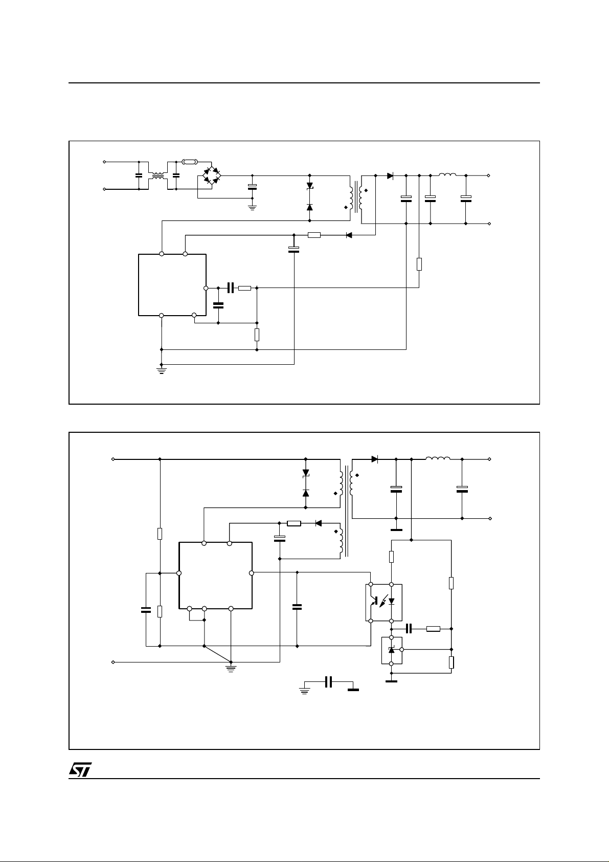
TYPICAL APPLICATION CIRCUIT
AC line
88 to 264 Vac
GND
DRAIN
L6590
1
Vcc
3
56, 7,8
4
VFBCOMP
Pout
up to 15W
DESCRIPTION
The L6590 is a monolithic switching regulator designed in BCD OFF-LINEtechnology, able to operate
with wide range input voltage and to deliver up to
15Woutput power. The internal power switch is a lateral power MOSFET with a typical R
and a V
AC line
88 to 264 Vac
(BR)DSS
of 700V minimum.
DRAIN
1
GND
L6590
VFB COMP
3
56, 7, 8
4
Vcc
DS(on)
of 13
Pout
up to 15W
Ω
October 2000
Primary Feedback
Secondary Feedback
1/23

L6590
D
DESCRIPTION
(continued)
The MOSFET is source-grounded, thus it is possible
to build flyback, boost and forward converters.
The device can work with secondary feedback and a
2.5V±2%internal reference,in addition to a high gain
error amplifier, makes possible also the use in applications either with primary feedback or not isolated.
Theinternalfixedoscillator frequencyandthe integrated
non dissipative start-up generator minimize the external
component count and power consumption.
The device is equipped with a standby function that
automatically reduces the oscillator frequency from
65 to 22 kHz under light load conditions to enhance
BLOCK DIAGRAM
DRAIN
(1)
[1]
START-UP
THERMAL
SHUTDOWN
+
-
GND
(6,7,8)
PGND
[9, ..., 16]
OCP
STANDBY
65/22kHz
efficiency (P
<1W@P
in
= 0.5W with wide range
out
mains).
Internal protections like cycle-by-cycle current limiting,
latched output overvoltage protection, mains undervoltage protection (SMD version only) and thermal shutdown generate a 'robust' design solution.
TheIC usesa special leadframe with the ground pins
(6, 7 and 8 in minidip, 9 to16 in SO16W package) internally connected in order for heat to be easily removed from the silicon die. An heatsink can then be
realized by simply making provision of few cm
copper on the PCB. Furthermore, the pin(s) close to
the high-voltage one are not connected to ease compliance with safety distances on the PCB.
[x] : L6590D (SO16W)
CC
V
(3)
SGN
[5]
BOK
[6]
VFB
(5)
[4]
[8]
OSC
SUPPLY
&UVLO
PWM
VREF
+
-
OVP
BROWNOUT
VREF
+
-
+
2.5V
2.5V
2
of
PIN CONNECTIONS
DRAIN
COMP
2/23
(Top view)
N.C.
Vcc
MINIDIP
L6590
GND
GND
GND
VFB
DRAIN
N.C.
N.C.
Vcc
SGND
BOK
COMP
VFB
COMP
[7]
(4)
PGND
PGND
PGND
PGND
PGND
PGND
PGND
PGND
SO16W
L6590D

L6590
PIN FUNCTIONS
Pin#
L6590 L6590D
1 1 DRAIN Drain connection of the internal power MOSFET. The internal high voltage start-up
2 2, 3 N.C. Not internally connected. Provision for clearance on the PCB.
34V
47
5 8 VFB Inverting input of the Error Amplifier.The non-inverting one is internally connected to a
6 to 8 - GND Connection of both the source of the internal MOSFET and the return of the bias current
- 6 BOK Brownout Protection. If the voltage applied to this pin is lower than 2.5V the PWM is
- 5 SGND Current return for the bias current of the IC.
- 9 to 16 PGND Connection of the source of the internal MOSFET. Pins connected to the metal frame to
Name Description
generator sinks current from this pin.
Supply pin of the IC. An electrolytic capacitor is connected between this pin and ground.
CC
The internal start-up generator charges the capacitor until the voltage reaches the startup threshold. The PWM is stopped if the voltage at the pin exceeds a certain value.
COMP
Output of the Error Amplifier. Used for control loop compensation or to directly control
PWM with an optocoupler.
2.5V± 2% reference. This pin can be grounded in some feedback schemes.
of the IC. Pins connected to the metal frame to facilitate heat dissipation.
disabled. This pin is typically used for sensing the input voltage of the converter through
a resistor divider. If not used, the pin can be either left floating or connected to Vcc
through a 15 kΩ resistor.
facilitate heat dissipation.
THERMAL DATA
Symbol Parameter Minidip SO16W Unit
R
thj-amb
R
thj-pins
(*) Value depending on PCB copper area and thickness
Thermal Resistance Junction to ambient (*) 35 to 60 40 to 65 °C/W
Thermal Resistance Junction to pins 15 20 °C/W
.
ABSOLUTE MAXIMUM RATINGS
Symbol Parameter Value Unit
V
I
V
I
clamp
P
T
T
stg
ds
d
cc
tot
Drain Source Voltage -0.3 to 700 V
Drain Current 0.7 A
IC Supply Voltage 18 V
VccZener Current 20 mA
Error Amplifier Ouput Sink Current 3 mA
Voltage on Feedback Input 5 V
BOK pin Sink Current 1 mA
Power Dissipation at T
2
, 2 oz copper dissipating area on PCB
3cm
Operating Junction Temperature -40 to 150 °C
j
< 50°C (Minidip and SO16W)
amb
1.5 W
Storage Temperature -40 to 150 °C
3/23

L6590
ELECTRICAL CHARACTERISTCS
(Tj= -25 to 125°C, Vcc= 10V; unless otherwise specified)
Symbol Parameter Test Condition Min. Typ. Max. Unit
POWER SECTION
V
(BR)DSS
I
R
DS(on)
Drain Source Voltage Id< 200 µA; Tj= 25 °C 700 V
Off state drain current Vds= 560V; Tj= 125 °C 200 µA
dss
Drain-to-Source on resistance
R
vs. Tj: see fig. 20
DS(on)
I
= 120mA; Tj=25°C 13 16 Ω
d
= 120mA; Tj= 125 °C 23 28
I
d
ERROR AMP SECTION
V
Input Voltage Tj= 25 °C 2.45 2.5 2.55 V
FB
= 125°C 2.4 2.5 2.6
T
j
Ib E/A Input Bias Current V
= 0 to 2.5 V 0.3 5 µA
FB
Avol DC Gain open loop 60 70 dB
B Unity Gain Bandwidth 0.7 1 MHz
SVR Supply voltage Rejection f = 120 Hz 70 dB
I
I
source
Output Sink Current V
sink
Output Source Current V
=1V 1 mA
COMP
= 3.5V; VFB = 2V -0.5 -1 -2.5 mA
COMP
V
COMPH
V
COMPL
Vout High I
Vout Low I
OSCILLATOR SECTION
F
D
D
Oscillator Frequency Tj=25°C 58 65 72 kHz
osc
Min. Duty Cycle V
min
Max. Duty Cycle V
max
DEVICE OPERATION SECTION
I
I
chargeVCC
V
CCclampVCC
V
Operating Supply Current fsw = Fosc 4.5 7 mA
op
I
Quiescent Current MOS disabled 3.5 6 mA
Q
charge Current Vcc=0VtoV
clamp Voltage I
Start Threshold
ccon
voltage
= -0.5mA; VFB=2V 3.8 4.50 V
source
= 1mA ; VFB=3V 1 V
sink
52 65 74
=1V 0 %
COMP
=4V 67 70 73 %
COMP
- 0.5V;
V
= 100 to 400V; Tj=25°C
ds
=0VtoV
V
cc
ccon
ccon
- 0.5V;
-3 -4.5 -7 mA
-2.5 -4.5 -7.5 mA
Vds= 100 to 400V
= 10mA (*) 16.5 17 17.5 V
clamp
(*) 14 14.5 15 V
V
4/23
V
ccoff
dsmin
Min operating voltage after Turnon(*) 6 6.5 7 V
Drain start voltage 40 V

L6590
ELECTRICAL CHARACTERISTICS
(continued)
Symbol Parameter Test Condition Min. Typ. Max. Unit
CIRCUIT PROTECTIONS
I
pklim
OVP Overvoltage Protection I
Pulse-by-pulse Current Limit di/dt = 120 mA/ µs 550 625 700 mA
= 10 mA (*) 16 16.5 17 V
cc
LEB Masking Time After MOSFET turn-on (**) 120 ns
STANDBY SECTION
F
I
pksb
Oscillator Frequency 19 22 25 kHz
SB
Peak switch current for Standby
Transition from F
osc
to F
SB
80 mA
Operation
I
pkno
Peak switch current for Normal
Transition from FSBto F
osc
190 mA
Operation
BROWNOUT PROTECTION (L6590D only)
V
I
V
Threshold Voltage Voltage either rising or falling 2.4 2.5 2.6 V
th
Current Hysteresis V
Hys
Clamp Voltage I
CL
= 3V -30 -50 -70 µA
pin
= 0.5 mA 5.6 6.4 7.2 V
pin
THERMAL SHUTDOWN (***)
Threshold 150 165 °C
Hysteresis 40 °C
(*) Parameters tracking one the other
(**) Parameter guaranteed by design, not tested in production
(***) Parameters guaranteed by design, functionality tested in production
Figure 1. Start-up & UVLO Thresholds Figure 2. Start-up Current Generator
Vcc [V]
16
14
Start-up
12
10
8
6
-50 0 50 100 150
Tj [°C]
UVLO
Icc [mA]
5.5
5
Vdrain = 40 V
4.5
4
3.5
3
024681012
Vcc [V]
Tj = -25°C
Tj = 25 °C
Tj = 125 °C
5/23

L6590
Figure 3 . Start-up Current Generator
Icc [mA]
5.5
Vdrain = 60 V
Tj = -25 °C
5
Tj = 25°C
4.5
4
Tj = 125°C
3.5
3
024681012
Vcc [V]
Figure 4. IC Consumption Before Start-up
Icc [µA]
700
600
500
400
300
200
Tj = 125°C
Tj = -25 °C
Tj = 25 °C
Figure 6. IC Operating Current
Icc [mA]
5
VFB = 2.3 V
fsw = 65 kHz
4.5
4
Tj = 125°C
Tj = 25 °C
Tj = -25°C
3.5
3
7 8 9 10 11 12 13 14 15
Vcc [V]
Figure 7. IC Operating Current
Icc [mA]
4.4
VFB = 2.3 V
4.2
4
3.8
3.6
3.4
3.2
fsw = 22 kHz
Tj = 125 °C
Tj = 25 °C
Tj = -25°C
100
7 8 9 101112131415
Vcc [V]
Figure 5. IC Quiescent Current
Icc [mA]
4
VFB = 2.7 V
3.8
3.6
3.4
Tj = 125°C
Tj = -25°C
3.2
3
6 8 10 12 14 16 18
Vcc [V]
6/23
Tj = 25°C
3
7 8 9 10 11 12 13 14 15
Vcc [V]
Figure 8. S witching Frequency vs.
Temperature
fsw [kHz]
80
70
60
50
40
30
20
10
-50 0 50 100 150
Normal operation
Standby
Tj [°C]

L6590
Figure 9 . Vcc clamp vs. Temperature
VCCclamp [V]
18
17.8
17.6
I
clamp
=20mA
17.4
Iclamp =10mA
17.2
17
-50 0 50 100 150
Tj [°C]
Figure 10. OV P Threshold vs. Temperature
Vth [V]
16
15.8
15.6
15.4
Figure 12. OCP threshold vs. Temperat ure
Ipklim / (Ipklim@ Tj = 25°C)
1.1
1.08
di/dt = 120 mA/µs
1.06
1.04
1.02
1
0.98
-50 0 50 100 150
Tj [°C]
Figure 13. Internal E/A Referenc e Voltage
Vref [V]
2.6
2.55
2.5
15.2
15
-50 0 50 100 150
Tj [°C]
Figure 11. OCP Threshold vs. Current Slope
Ipklim / (Ipklim @ di/dt = 120 mA/µs)
1.06
1.04
1.02
1
0.98
0.96
50 100 150 200 250
Tj = 25°C
dI/dt[mA/µs]
2.45
2.4
-50 0 50 100 150
Tj [°C]
Figure 14. Error Amplifier Slew Rate
VCOMP [V]
5
= 100 pF
L
open loop
Ω
4
3
VCOMP
V
FB
RL =10k
C
2
1
0
0 2 4 6 8 10121416
t[µs]
7/23

L6590
Figure 15. COMP pin Characteristic
VCOMP [V]
6
VFB =0
5
Tj = 25 °C
4
3
2
1
0
0 0.2 0.4 0.6 0.8 1 1 .2 1.4
ICOMP [mA]
Figure 16. COM P pin Dynamic Resistance vs.
Temperature
RCOMP[kOhm]
10.5
10
VFB =0
Figure 18. Breakdown Voltage vs. Temperature
BVDSS / (BVDSS @ Tj = 25°C)
1.08
1.06
Idrain = 200 µA
1.04
1.02
1
0.98
0.96
0.94
0.92
-50 0 50 100 150
Tj [°C]
Figure 19. Drain Leakage vs. Drain Voltage
Idrain [µA]
50
40
Tj = 125 °C
Tj = 25 °C
9.5
9
8.5
8
-50 0 50 100 150
Tj [°C]
Figure 17. Error Amplifier Gain and Phase
dB
100
50
0
Phase
Gain
1 10 100 1k 10k 100k
1M
f[Hz]
m
φ
90
180
30
Tj = -25°C
20
10
100 200 300 400 500 600 700
Vdrain [V]
Figure 20. Rds(ON) vs. Tempe rature
Rds(ON) / (Rds(ON) @ Tj=25°C)
1.8
°
0
1.6
Idrain = 120 mA
1.4
1.2
1
0.8
0.6
-50 0 50 100 150
Tj [°C]
8/23
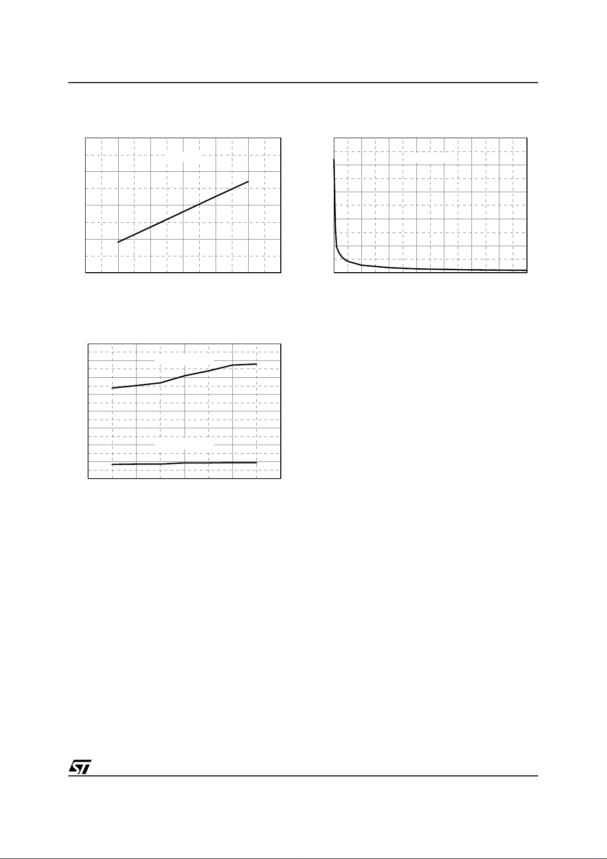
Figure 21. Rds(ON) vs. Idrain Figure 22. Coss vs. Drain Voltage
L6590
Rds(ON) / (Rds(ON) @ Idrain=120 mA)
1.3
Tj = 25 °C
1.2
1.1
1
0.9
0 100 200 300 400 500 600
Idrain [mA]
Figure 23. Standby Function Thresholds
DrainPeak Current[mA]
220
200
180
160
140
120
100
80
60
-50 0 50 100 150
22 kHz → 65 kHz
65 kHz→22 kHz
Tj [°C]
Coss [pF]
250
200
Tj = 25 °C
150
100
50
0
0 100 200 300 400 500 600 700
Vdrain [V]
9/23
L6590
)
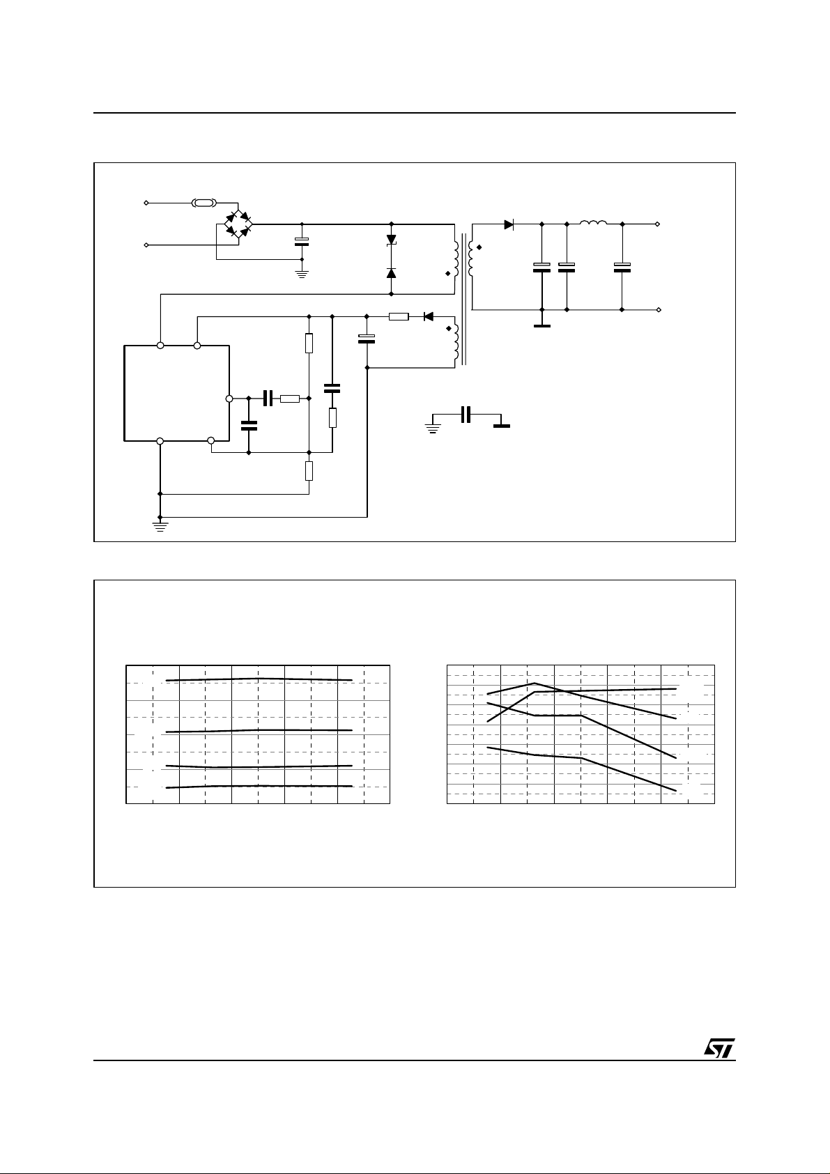
Figure 24. Test Board (1) with Primary Feedback: Electri cal Schematic
F1
Vin
88 to 264 Vac
L6590
6, 7, 8
2A/250V
IC1
31
4
5
BD1
DF06M
C5
680 nF
C1
22 µF
400 V
5.6 kΩ
1.1 kΩ
C6
10 nF
R2
R3
BZW06-154
STTA106
100 nF
110
R4
1.5 kΩ
C4
R5
D1
D2
Ω
T1
D4 BYW100-100
C7, C8
330 µF
16 V
R1 68 Ω
D3
C2
1N4148
22 µF
25 V
C7
2.2 nF
Y
T1 specification
Core E20/10/6, ferrite 3C85 or N67 or equivalent
≈
0.5 mm gap for a primary inductance of 2.9 mH
leakage
<90 µH
L
Primary : 180 T, 2 series windings 90T each, AWG33(∅0.22 mm
Sec : 19 T, AWG30 (∅0.3 mm)
Aux : 19 T, AWG33
L1
4.7 µH
C9
100 µF
16 V
Vo =12 V ± 10%
Po= 1 to 10 W
Figure 25. Test Board (1) Evaluation Data
Output Voltage [V]
13.5
1W
13
2.5 W
12.5
5W
12
out =
P
10 W
11.5
50 100 150 200 250 300
Load & Line regulation
Input Voltage[Vac]
Efficiency [%]
Efficiency
86
out =
84
82
80
P
10 W
5W
78
76
74
72
50 100 150 200 250 300
InputVoltage [Vac]
2.5 W
1W
10/23

Figure 26. Test Board (1) Main Waveforms
Ch3: Idrain
L6590
Ch3: Idrain
Vin=100V
DC
Pout = 10 W
Ch2: Vdrain
Ch3: Idrain
Ch2: Vdrain
Vin = 100 V
Pout = 1 W
DC
Ch2: Vdrain
Ch3: Idrain
Ch2: Vdrain
Figure 27. Test Board (2) with Secondary Feedback: Electrical Schematic
F1
2A/250V
Vin
88 to 264
Vac
Cx
100 nF
L
A
22 mH
CxB
100 nF
6, 7, 8
IC1
L6590
BD1
DF06M
31
5
C1
22 µF
400 V
4
STT A106
C2
22 µF
25V
D2
R1 10
D1
BZW06-154
Ω
D3
1N4148
C3
22 nF
6.8 k
T1
OP1
PC817
R6
Ω
C4
2.2 nF
Y1
class
D4 1N5822
C5, C6, C7
470 µF
16V
RubyconZL
4
3
1
2
560
1
2
3
R2
100 nF
TL431
Ω
C9
IC2
2k
R5
L1
4.7 µH
C8
220 µF
10V
Rubycon
ZL
Ω
Vin=400V
Pout = 10 W
Vin=400V
Pout = 1 W
5Vdc/2A
R3
Ω
2.43 k
R4
Ω
2.43 k
DC
DC
Core E20/10/6,ferrite 3C85 or N67 or equivalent
T1 specification
≈
0.6 mm gap for a primary inductance of 1.4 mH
leakage
<30 µH
L
Primary : 128 T, 2 series windings64T each, AWG32(∅0.22mm)
Sec : 6 T, 4xAWG32
Aux : 14 T, AWG32
11/23
L6590
Figure 28. Te st B oard (2) evaluation data
Output Voltage [V]
Load & Line regulation
5
4.98
4.96
AC
4.94
4.92
4.9
0.003 0.01 0.03 0.1 0.3 1 3
Input Power [mW]
Light-load Consumption
Load Current [A]
220 V
110 V
AC
1,000
800
600
400
200
0
50 100 150 200 250 300 350 400 450
DC InputVoltage [V]
264 V
88 V
AC
AC
out
P
0.5W
0.25W
0.1W
0.05W
0W
Efficiency [%]
80
Efficiency
88 VAC
70
60
AC
110 V
50
264 V
AC
220V
AC
40
30
20
0.003 0.01 0.03 0.1 0.3 1 3
Pdiss [W]
5
Rthj-amb= 58 °C/W @ 1.5W
2
Load Current [A]
Device Power Dissipation
AC
264 V
88 V
1
AC
0.5
0.2
220 V
110 V
0.1
0.05
0.003 0.01 0.03 0.1 0.3 1 3
Load Current [A]
AC
AC
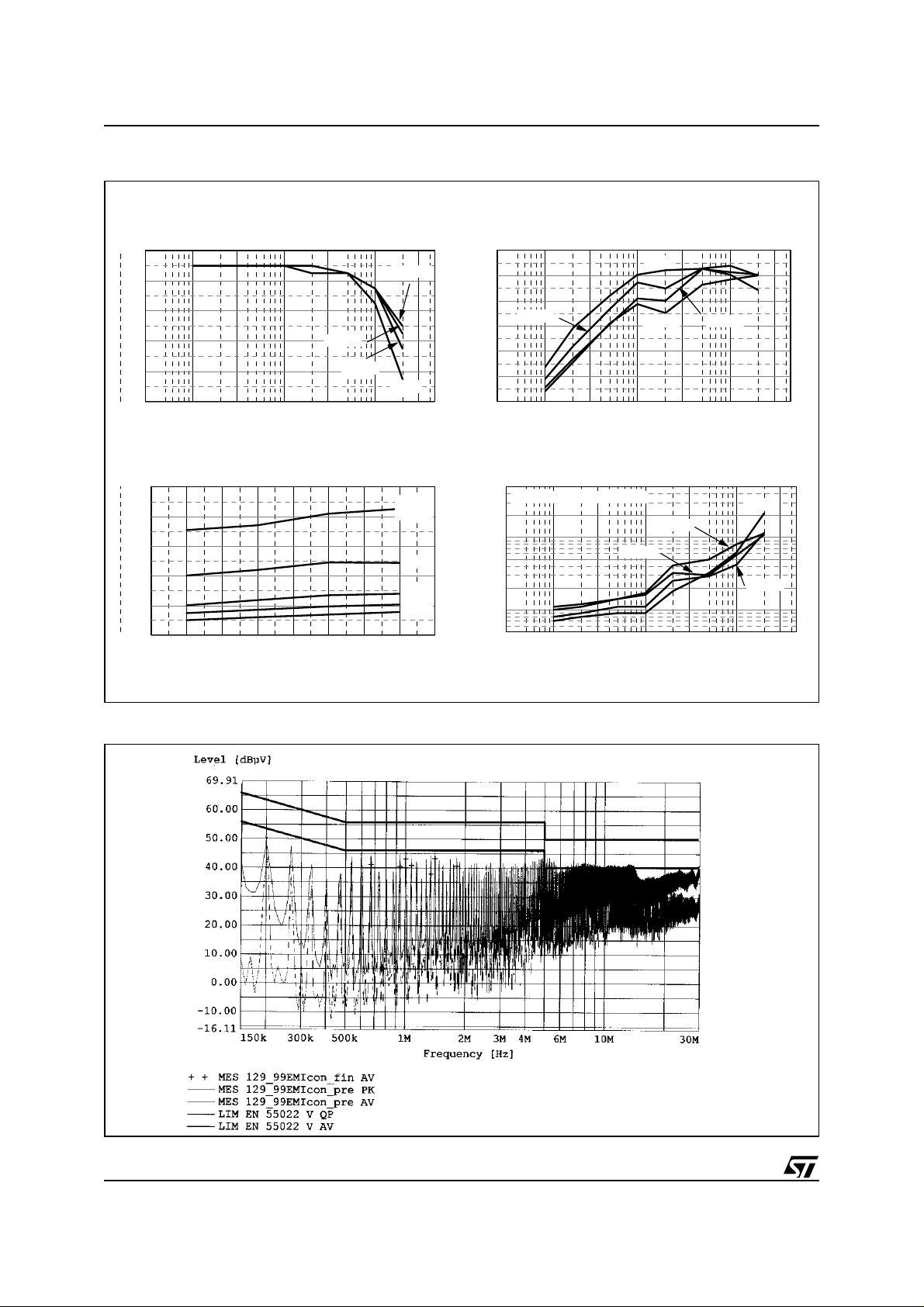
Figure 29. Te st B oard (2) EMI Characterization
12/23
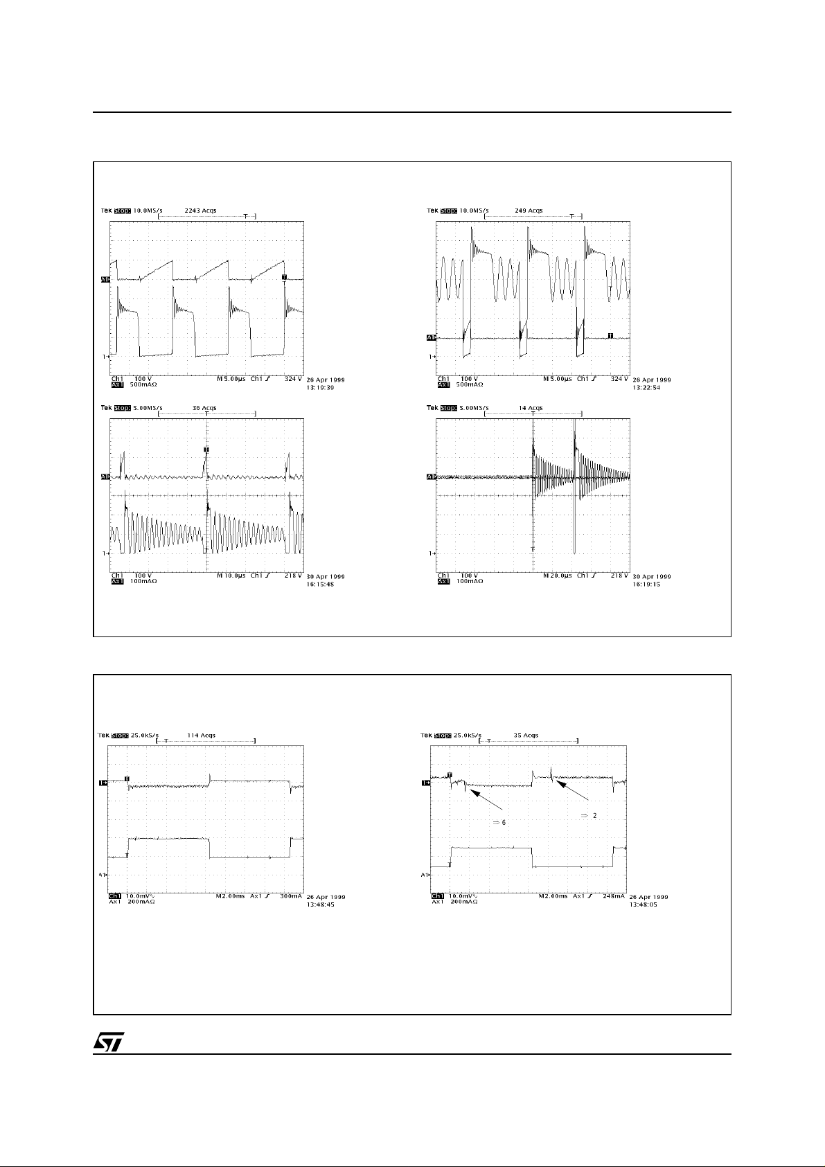
Figure 30. Test Board (2) Main Waveforms
A1: Idrain
L6590
Ch1: Vdrain
Vin=100V
DC
Iout = 2 A
Ch1: Vdrain
A1: Idrain
Vin=100V
DC
Iout = 50 mA
Ch1: Vdrain
Figure 31. Test Board (2) Load Transient Response
A1: Idrain
A1: Idrain
Ch1: Vdrain
Vin = 400 V
Iout = 2 A
Vin = 400 V
Iout = 50 mA
DC
DC
Vout
Standby Function
is not tripped
Iout
Vin = 200 V
DC
Iout = 0.2↔0.4 A
transition
⇒
22
65 kHz
Standby Function
is tripped
Vout
65
Iout
transition
⇒
22 kHz
Vin=200V
DC
Iout= 0.1↔0.3 A
13/23

L6590
APPLICATION INFORMATION
In the following sections the functional blocks as well as the most important internal functions of the device will
be described.
Start-up Circuit
When power is first applied to the circuit and the voltage on the bulk capacitor is sufficiently high, an internal
high-voltage current generator is sufficiently biased to start operating and drawing about 4.5 mA through the
primary winding of the transformer and the drainpin. Most of this current charges the bypass capacitor connected between pin Vcc (3) and ground and makes its voltage rise linearly.
As the Vcc voltage reaches the start-up threshold (14.5V typ.) the chip, after resetting all its internal logic, starts
operating, the internal power MOSFET is enabled to switch and the internal high-voltage generator is disconnected. The IC is powered by the energy stored in the Vcc capacitor until the self-supply circuit (typically an
auxiliary windingof the transformer) developsa voltagehighenough to sustain the operation.
As the IC is running, the supply voltage, typically generated by a self-supply winding, can range between 16 V
(Overvoltage protection limit, see the relevant section) and 7 V, threshold of the Undervoltage Lockout. Below
this value the device is switched off (and the internal start-up generator is activated). The two thresholds are in
tracking.
The voltage on the Vcc pin is limited at safe values by a clamp circuit. Its 17V threshold tracks the Overvoltage
protection threshold.
Figure 32. Start-up circu it internal schematic
DRAIN
POWER
MOSFET
GND
Vcc
15 M
UVLO
Ω
17 V
150
Ω
Power MOSFET and Gate Driver
The power switch is implemented with a lateral N-channel MOSFET having a V
ical R
of 13Ω. It has a SenseFET structure to allow a virtually lossless current sensing (used only for pro-
DS(on)
(BR)DSS
of 700V min. and a typ-
tection).
During operation in Discontinuous Conduction Mode at low mains thedrain voltage is likely to go belowground.
Any risk of injecting the substrate of the IC is prevented by an internal structure surrounding the switch.
The gate driver of the power MOSFET is designed to supply a controlled gate current during both turn-on and
turn-off in order to minimize common mode EMI.
Under UVLO conditions an internal pull-down circuit holds the gate low in order to ensure that the power MOS-
FET cannot be turned on accidentally.
14/23

Figure 33. PWM Control internal schematic
L6590
Max.Duty cycle
E/A
+
-
S
R
from OCP
comparator
VFB
to gate
Q
driver
OSCILLATOR
+
PWM
-
COMP
Clock
Oscillator and PWM Control
PWMregulation is accomplished by implementingvoltage modecontrol. As shown in fig. 33, this block includes
an oscillator, a PWM comparator, a PWM latch and an Error Amplifier.
The oscillator operates at a frequency internally fixed at 65 kHz with a precision of ± 10 %. The maximum duty
cycle is limited at 70% typ.
The PWM latch (reset dominant) is set by the clock pulses of theoscillator and is reset by either the PWM comparator or the Overcurrent comparator.
The Error Amplifier (E/A) is an op-amp with a MOS input stage and a class AB output stage. The amplifier is
compensated for closed loop stability at unity gain, has a small-signal DC gain of 70 dB (typ.) and a gain-bandwidth product over 1 MHz.
In case of overcurrent the error amplifier output saturates high and the conduction of the power MOSFET is
stopped by the OCP comparator instead of the PWM comparator.
Under zero load conditions the error amplifier is close to its low saturation and the gate drive delivers as short
pulses as it can, limited by internal delays. They are howevertoo longto maintainthe long-termenergy balance,
thus from time to time some cycles need being skipped and the operation becomes asynchronous. This is automatically done by the control loop.
Standby Function
The standby function, optimized for flyback topology, automatically detects a light load condition for the converter and decreasestheoscillator frequency. The normal oscillationfrequency is automatically resumed when the
output load builds up and exceeds a defined threshold.
This function allows to minimize power losses related to switching frequency, which represent the majority of losses
in a lightly loaded flyback, without giving up the advantages of a higher switching frequency at heavy load.
The Standby function is realizedby monitoringthe peak current in the power switch. If the loadis low that it does
not reach a threshold (80 mA typ.), the oscillator frequency will be set at 22 kHz typ.
When the load demands more power and the peak primary current exceeds a second threshold (190 mA typ.)
theoscillator frequency is reset at 65 kHz. This 110 mA hysteresis prevents undesired frequency change when
power is such that the peak current is close to either threshold.
The signal coming from the sense circuit is digitally filtered to avoid false triggering of this function as a result of
large load changes or noise.
15/23

L6590
Figure 34. Standby Function timing diagram
Pout
Peak
80 mA
190mA
Primary
Current
Load
regulation
Vout
small glitch
STANDBY
(before filter)
STANDBY
2ms 1ms
(filtered)
65 kHz
sw
f
22 kHz
Brownout Protection (L6590D only)
Brownout Protection is basically a not-latched device shutdown functionality. It will typically be used to detect a
mains undervoltage (brownout). This condition may cause overheating of the primary power section due to an
excess of RMS current.
Figure 35. Brownout Protection Function internal schematic an d timing diagram
HV Input bus
ON
V
OFF
V
16/23
HV Input bus
BOK
50 µA
6.4 V
2.5 V
Vcc
+
-
VinOK
L6590D
VinOK
Vcc
PWM
Vout

L6590
Another problem is the spurious restarts that are likely to occur during converter power down if the input voltage
decays slowly (e.g. with a large input bulk capacitor) and that cause the output voltage not to decay to zero
monothonically.
Converter shutdown can be accomplished with the L6590D by means of an internal comparator that can be
used to sense the voltage across the input bulk capacitor. This comparator is internally referenced to 2.5V and
disables the PWM if the voltage applied at its non-inverting input, externally available, is below the reference.
PWM operation is re-enabled as the voltage at the pin is more than 2.5V.
The brownout comparator is provided with current hysteresis instead of a more usual voltage hysteresis: an internal 50 µA current generator is ON as long as the voltage applied at the non-inverting input exceeds 2.5V and
is OFF if the voltage is below 2.5V. This approach provides an additional degree of freedom: it is possible to set
the ON threshold and the OFF threshold separately by properly choosing the resistors of the external divider,
which is not possible with voltage hysteresis.
Overvoltage Protection
The IC incorporatesan Overvoltage Protection (OVP) thatcan be particularly useful to protect the converter and
the load against voltage feedback loop failures. This kind of failure causes the output voltage to rise with no
control and easily leads to the destruction of the load and of the converter itself if not properly handled.
If such an event occurs, the voltage generated by the auxiliary winding that supplies the IC will fly up tracking
the output voltage. An internal comparator continuously monitors the Vcc voltage and stops the operation of the
IC if the voltage exceeds 16.5 V. This condition is latched and maintained until the Vcc voltage falls below the
UVLO threshold. The converter will then operate intermittently.
Figure 36. OVP internal schematic
Vcc DRAIN
to
MOSFET
to OVP
+
OVP
-
latch
GND
Overcurrent Protection
Thedevice uses pulse-by-pulse current limiting for Overcurrent Protection (OCP), in order to prevent overstress
of the internal MOSFET: its current during the ON-time is monitored and, if it exceeds a determined value, the
conductionis terminated immediately. TheMOSFETwillbe turned on again in the subsequentswitchingcycle.
As previously mentioned, the internal powerMOSFET has a SenseFET structure: the source of a few cells are
connectedtogether and kept separate from the othersourceconnections so as to realize a 1:100 current divider.
The "sense" portion is connected to a ground referenced, sense resistor having a low thermal coefficient. The
OCP comparator senses the voltage drop across the sense resistor and resets the PWM latch if the drop exceeds a threshold, thus turning off the MOSFET. In this way the overcurrent threshold is set at about 0.65 A
(typical value).
17/23

L6590
At turn-on, there are large current spikes due to the discharge of parasitic capacitances and, in case of Continuos Conduction Mode operation, to secondary diode reverse recovery as well, which could falsely trigger the
OCP comparator. To increase noise immunity the output of the OCP comparator is blanked for a short time
(about120 ns) just after the MOSFETis turnedon, so that any disturbancewithin this time slotis rejected(Leading Edge Blanking).
Figure 37. OCP internal schem atic
DRAIN
Max. Duty cycle
OSCILLATOR
+
PWM
-
Clock
Clock
S
R
Q
OCP
LEB
Driver
1
1/100
+
Rsense
-
0.5 V
GND
Thermal Shutdown
Overheating of the device due to an excessive power throughput or insufficient heatsinking is avoided by the
Thermal Shutdown function. A thermal sensor monitors the junction temperature close to the power MOSFET
and, when the temperature exceeds 150 °C (min.), sets an alarm signal that stops the operation of the device.
This is a not-latched function and the power MOSFET is re-enabled as the temperature falls about 40 °C.
18/23
APPLICATION IDEAS
Figure 38. 10W AC-DC adapter with no isolation
F1
2A/250V
Vin
88 to 264 Vac
Cx
100 nF
A
L
22 mH
100 nF
3(4)1
L6590
(L6590D)
6, 7, 8
(9 to16)
CxB
5(8)
BD1
DF06M
C1
22 µF
400 V
IC1
C4
R3
100 nF
4
(7)
27 k Ω
C5
2.2 nF
BZW06-154
STTA106
R4
1kΩ
D1
D2
R1 10 Ω
C2
22 µF
25 V
T1
D3
1N4148
D4 S TPS3L60S
C7, C8
330 µF
16 V
R2
3.9 kΩ
L1
4.7 µH
C9
100 µF
16 V
Vo =12 V ± 3%
Io= 0 to 0.8 A
L6590
Figure 39. 15W Auxiliary SMPS for PC
Vin = 200 to 375 Vdc
R2
Ω
1.8 M
41
IC1
67
L6590D
9,..., 16
5
R3
20 k
8
Ω
C1
10 nF
BZW06-154
STTA106
C2
22 µF
25 V
D1
D2
R1 10
Ω
1N4148
C3
47 nF
Core E20/10/6, ferrite 3C85 or N67 or equivalent
≈
0.5 mm gap for a primary inductance of 1.6 mH
leakage
L
<30 µH
Primary : 130 T, 2series windings65T each, AWG33(∅0.22 mm)
T1 specification
Sec : 14 T,AWG26(∅0.4 mm)
T1
D4 STPS10L25D
C5, C6, C7
470 µF
10 V
L1
4.7 µH
C8
100 µF
10V
5Vdc/3A
D3
R4
Ω
560
R5
Ω
2.43 k
1
4
470 nF
IC2
TL431
C9
240
R7
Ω
R6
2.43 k
3
2
1
3
2
C4
2.2 nF
Y
OP1
PC817
Ω
CoreE20/10/6, ferrite 3C85or N67 or equivalent
≈
0.9 mm gap for a primary inductance of 2 mH
leakage
<50 µH
L
T1 specification
Primary : 200 T, 2 serieswindings 100T each, AWG33(∅0.22 mm)
Sec : 9 T, 2 xAWG23 (∅0.64 mm)
Aux : 21 T,AWG33
19/23

L6590
,
Figure 40. 7.2V/7W Battery Charger
Vin
88 to 264 Vac
A
Cx
100 nF
L6590
(L6590D)
6, 7, 8
(9 to 16)
F1
2A/250V
L
22 mH
CxB
100 nF
R2
Ω
5.6 k
3(4)1
5
(8)
4(7)
R4 10 kΩ
C3 10 nF
Core E20/10/6, ferrite 3C85 or N67 or equivalent
≈
1 mm gap for a primary inductance of 2.6 mH
leakage
L
<60 µH
Primary : 230 T, 2 series windings 115T each, AWG36(∅0.16 mm)
Sec : 13 T, AWG23 (∅0.64 mm)
Aux : 60 T
AWG36
BD1
DF06M
22 µF
400 V
R1
39
Ω
C3
10 µF
25V
R3
Ω
1.5 k
T1 specification
C1
D2
STTA106
34
C2
220 nF
BZW06-154
OP1
PC817
C4
2.2 nF
Y1 class
D1
D3 BAV21
T1
16:1
R12
1k
D4 1N5821
1
2
Ω
1N4148
C5, C6
330 µF
16V
R7
620
1N4148
1N4148
D6
D7
D5
Ω
R5
4.7 k
D8
BZX79C12
R6
Ω
0.1
R8
560
C8 680 nF
R11
11.8 k
5
7
Ω
Ω
Ω
6
IC2
TSM103
421
C9 330 nF
Q1
BC337
22.6 k
R10
Ω
6.8 k
8
3
C7
10 µF
25V
R9
Ω
7.2 Vdc / 1 A
R13
12 k
Ω
REFERENCES
[1] “Getting Familiar with the L6590 Family, High-voltage Fully Integrated Power Supply” (AN1261)
[2] “Offline Flyback Converters Design Methodology with the L6590 Family” (AN1262)
20/23

L6590
21/23
L6590
22/23

L6590
Information furnished is believed to be accurate and reliable. However, STMicroelectronics assumes no responsibility for the consequences
of use of such information nor for any infringement of patents or other rights of third parties which may resultfrom its use. No licenseisgranted
by implication or otherwise under any patent or patent rights of STMicroelectronics. Specifications mentioned in this publication are subject
to change without notice. This publication supersedes and replaces all information previously supplied. STMicroelectronics products are not
authorized for use as critical components in life support devices or systems without express written approval of STMicroelectronics.
The ST logo is a registered trademark of STMicroelectronics
2000 STMicroelectronics - All Rights Reserved
Australia - Brazil - China - Finland - France - Germany - Hong Kong - India - Italy - Japan - Malaysia - Malta - Morocco - Singapore - Spain
STMicroelectronics GROUP OF COMPANIES
- Sweden - Switzerland - United Kingdom - U.S.A.
http://www.st.com
23/23
 Loading...