

CFL/TL BALLAST DRIVER PREHEAT AND DIMMING
■ HIGH VOLTAGE RAIL UP TO 600V
■ dV/dt IMMUNITY ± 50 V/ns IN FULL
TEMPERATURE RANGE
■ DRIVER CURRENT CAPABILITY:
250mA SOURCE
450mA SINK
■ SWITCHING TIMES 80/40ns RISE/FALL
■ WITH 1nF LOAD
■ CMOS SHUT DOWN INPUT
■ UNDER VOLTAGE LOCK OUT
■ PREHEAT AND FREQUENCY SHIFTING
TIMING
■ SENSE OP AMP FOR CLOSED LOOP
CONTROL OR PROTECTION FEATURES
■ HIGH ACCURACY CURRENT CONTROLLED
OSCILLATOR
■ INTEGRATED BOOTSTRAP DIODE
■ CLAMPING ON VS.
■ SO16, DIP 16 PACKAGES
DESCRIPTION
In order to ensure voltage ratings in excess of
600V, the L6574 is manufactured with BCD OFF
LINE technology, which makes it well suited for
lamp ballast applications.
L6574
SO16N DIP16
ORDERING NUMBERS:
L6574D L6574
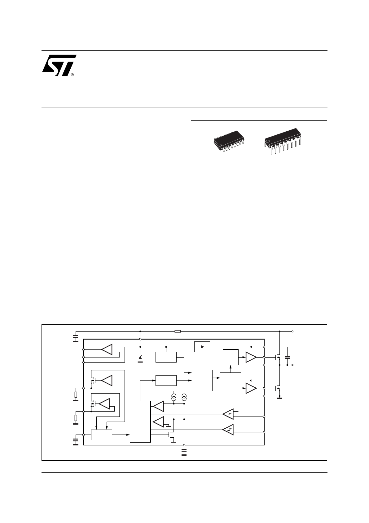
The device is intended to drive two power MOSFETS, in the classical half bridge topology, ensuring all the features needed to drive and properly
control a fluorescent bulb.
A dedicated timing section in the L6574 allows the
user set the necessary parameters for proper preheat and ignition of the lamp.
Also, an OP AMP is available to implement closed
loop control of the lamp current during normal
lamp burning.
An in teg rat ed boo tst r ap s ect io n, e li min ati ng th e no rmally required bo otstra p diode an d the zener clamping on Vs, makes the L6574 well suited for low cost
applica tions where few ad ditional co mponents are
needed to build a high performance ballast.
BLOCK DIAGRAM
OPOUT
OPIN-
OPIN+
R
ING
R
PRE
Cf
September 2003
OP AMP
Imin
Imax
VCO
V
S
V
+
-
V
REF
V
REF
CONTROL
LOGIC
UV
DETECTION
DEAD
TIME
Ifs
+
Vthpre
-
+
-
Ipre
DRIVER
DRIVING
LOGIC
C
PRE
HVG
DRIVER
LEVEL
SHIFTER
LVG DRIVER
+
-
+
-
V
V
THE
V
THE
D97IN493A
BOOT
HVGBOOTSTRAP
OUT
S
LVG
GND
EN1
EN2
H.V.
C
BOOT
LOAD
1/10
L6574
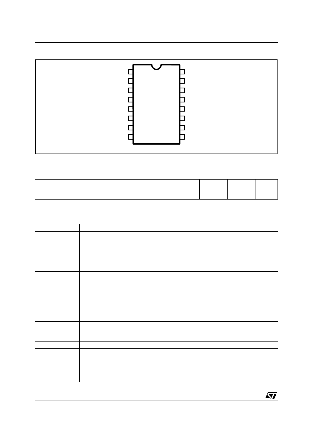
PIN CONNECTION (top view)
CPRE
RPRE
CF
RING
OPOUT
OPIN-
OPIN+
1
2
3
4
5
6
7 GND
15
14
13
12
11
10
VBOOT16
HVG
OUT
N.C.
V
S
LVG
EN1 8 EN29
D97IN492
THERMA L D ATA
Symbol Parameter DIP16 SO16N Unit
R
th j-amb
Thermal Resistance Junction to ambient Max. 80 120 °C/W
PIN DESCRIPTION
N° Pin Function
1 CPRE Preheat Timing Capacitor. The capacitor C
according to the relations: t
PRE
= K
PRE
· C
0.15s/µF). This feat ure is obtained by chargin g CPRE with two different cu rrents. During tPRE
this current is independent of the external components, so CPRE is charged up to 3.5V (preheat
timing comparato r threshol d). During t
ence between f
PRE
and f
). In this way tSH is always set at 0.1t
IGN
SH
at pin 1 is 5V.
2 RPRE Maximum Oscillation Frequency Setting. The resistance connected between this pin and ground
sets the fPRE value, fixing the difference betwe en f
Start-up procedure, the effect current drown from R
V
=2V.
REF
3 CF Oscillator Frequency Setting. The capacitor C
In normal operation this pin shows a triangular wave.
4 RIGN Minimum Oscilla tion Fre quen cy Set ting. Th e resis tance connect ed betw een th is pin a nd grou nd
sets the f
value. The voltage at this pin is fixed at V
IGN
5 OPout Out of the operational amplifier. To implement a feedback control loop this pin can be connected
to the RIGN pin by means an appropriate circuitry.
6 OPin- Inverting Input of the operational amplifier.
7 OPin+ Non Inverting Input of the operational amplifier.
8 EN1 Enable 1. This pin (active high), forces the device in a latched shutdown state (like in the under
voltage conditions). There are two ways to resume normal operation:
– the first is to reduce the supply voltage below the undervoltage threshold and then
increase it again until the valid supply is recognised.
– the second is activating EN2 input.
The enable 1 is especially designed for strong fault (e.g. in case of lamp disconnection).
sets the preheating a nd the frequ ency shift tim e,
PRE
and tSH = KFS · C
PRE
the curren t depends on R
and f
PRE
is over. The voltage at this pin is fixed at
PRE
, along with to R
F
=2V.
REF
(typ. K
PRE
PRE
. In steady state the voltage
PRE
(f
PRE
> f
PRE
and R
IGN
= 1.5s/µF, KFS =
PRE
value (i.e. on the differ-
). At the end of the
IGN
, sets f
IGN
PRE
and f
ING
.
2/10
PIN DESCRIPTION (continued)
N° Pin Function
9 EN2 Enable 2. EN2 input (active high) restarts the start-up procedure (preheating and ignition
sequence). This features is useful if the lamp does not turn-on after the first ignition sequence .
10 GND Ground.
11 LVG Low Side Driver Output. This pin must be connected to the low side power MOSFET gate of the
half bridge. A resistor connected b etween this pin and the p ower MOS gate can be used to
reduce the peak current.
12 VS Supply Voltage. This pin, connected to the supply filter capacitor, is internally clamped (15.6V
typical).
13 N.C. Non Connected. This pin set a distance between the pins related to the HV and those rela ted to
the LV side.
14 OUT High Side Driver Floating Reference. This pin must be connected close to the source of the high
side power MOS or IGBT.
15 HVG High Side Driver Output. This pin must be connected to the high side power MOSFET gate of the
half bridge. A resistor connected b etween this pin and the p ower MOS gate can be used to
reduce the peak current.
16 VBOOT Bootstrapped Supply Voltage. Between this pin and VS must be connected the bootstrap capac-
itor. A patented integrated cir cuitry replaces the exte rnal bootstrap diode, by m eans of a high
voltage DMOS, synchronously driven with the low side power MOSFET.
L6574
ABSOLUTE MAXIMUM RATINGS
Symbol Parameter Value Unit
I
S
V
LVG
V
OUT
V
HVG
V
BOOT
dV
BOOT
dV
OUT
V
V
, V
V
EN1
, I
I
EN1
V
opc
V
opd
V
opo
T
stg
T
amb
(*) The device has an internal Clamping Zener between GND and the V
Supply Current (*) 25 mA
Low Side Output -0.3 to Vs +0.3 V
High Side Reference -1 to VBOOT -18 V
High Side Output -1 to VBOOT V
Floating Supply Voltage -1 to 618 V
/dt V
pin Slew rate (repetitive) ±50 V/ns
BOOT
/dt OUT pin Slew Rate (repetitive) ±50 V/ns
Forced Input Voltage (pins Ring, Rpre) -0.3 to 5 V
ir
Forced Input Voltage (pins Cpre, Cf) -0.3 to 5 V
ic
Enable Input Voltage -0.3 to 5 V
EN2
Enable Input Current ±3mA
EN2
Sense Op Amp Common Mode Range -0.3 to 5 V
Sense Op Amp Differential Mode Range ±5V
Sense Op Amp Output Voltage (forced) 4.6 V
, TjStorage Temperature -40 to +150 °C
Ambient Temperature -40 to +125 °C
pin, it must not be supplied by
CC
a Low Impedance Voltage Source.
Note: ESD immunity for pins 14, 15 and 16 is guaranteed up to 900V (Human Body Model)
3/10
 Loading...