

■ HIGH VOLTAGE RAIL UP TO 600V
■ BCD OFF LINE TECHNOLOGY
■ 15.6V ZENER CLAMP ON V
■ DRIVER CURRENT CAPABILITY:
S
- SINK CURRENT = 270mA
- SOURCE CURRENT = 170mA
■ VERY LOW START UP CURRENT: 150µA
■ UNDER VOLTAGE LOCKOUT WITH
HYSTERESIS
■ PROGRAMMABLE OSCILLATOR
FREQUENCY
■ DEAD TIME 1.25µs (L6571A) or 0.72µs
(L6571B)
■ dV/dt IMMUNITY UP TO ±50V/ns
■ ESD PROTECTION
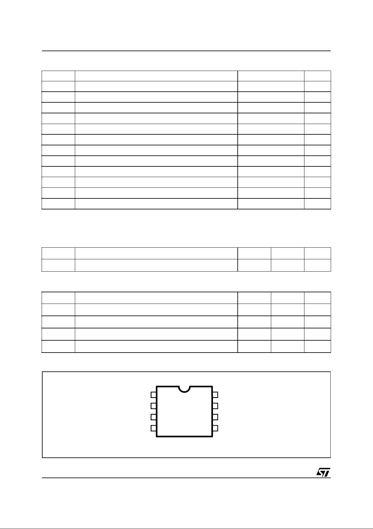
DESCRIPTION
The device is a high voltage half bridge driver with
built in oscillator. The frequency of the oscillator can
be programmed using external resistor and capaci-
L6571A
L6571B
HIGH VO LTAGE HALF BRIDGE
DRIVER WITH OSCILLATOR
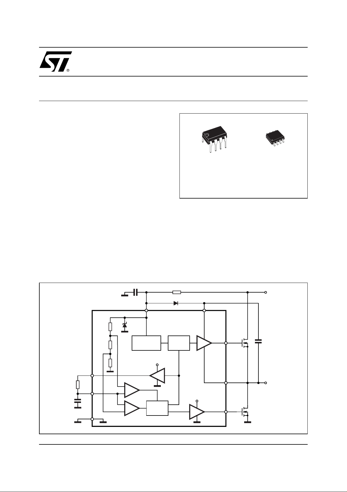
Minidip SO8
ORDERING NUMBERS:
L6571A L6571AD
L6571B L6571BD
tor. The internal circuitry of the device allows it to be
driven also by external logic signal.
The output drivers are designed to drive external nchannel power MOSFET and IGBT. The internal logic assures a dead time to avoid cross-conduction of
the power devices.
Two version are available: L6571A and L6571B.
They differ in the internal dead time: 1.25
µ
s(typ.)
0.72
µ
s and
BLOCK DIAGRAM
R
R
F
C
C
F
GND
September 2000
D96IN433
C
H.V.
BOOT
LOAD
R
C
VS
S
1
BIAS
REGULATOR
V
S
2
F
3
F
4
COMP
COMP
BUFFER
LOGIC
HV
LEVEL
SHIFTER
BOOTV
8
V
S
LOW SIDE
HIGH
SIDE
DRIVER
DRIVER
7
HVG
6
OUT
LVG
5
1/8
L6571A L6571B
ABSOLUTE MAXIMUM RATINGS
Symbol Parameter Value Unit
(*) Supply Current 25 mA
I
S
V
CF
V
LVG
V
OUT
V
HVG
V
BOOT
V
BOOT/OUT
dV
BOOT
dV
OUT
T
stg
T
T
amb
(*)The device has an internal zener clamp between GND and VS (typical 15.6V).Therefore the circuit should not be driven by a DC low im-
pedance power source.
Note: ESD immunity for pins 6, 7 and 8 is guaranteed up to 900 V (Human Body Model)
Oscillator Resistor Voltage 18 V
Low Side Switch Gate Output 14.6 V
High Side Switch Source Output -1 to V
High Side Switch Gate Output -1 to V
-18 V
BOOT
BOOT
Floating Supply Voltage 618 V
Floating Supply vs OUT Voltage 18 V
/dt VBOOT Slew Rate (Repetitive) ± 50 V/ns
/dt VOUT Slew Rate (Repetitive) ± 50 V/ns
Storage Temperature -40 to 150 °C
Junction Temperature -40 to 150 °C
j
Ambient Temperature (Operative) -40 to 125 °C
V
THERMAL DATA
Symbol Parameter Minidip SO8 Unit
R
th j-amb
Thermal Resistance Junction-Ambient Max 100 150 °C/W
RECOMMENDED OPERATING CONDITIONS
Symbol Parameter Min. Max. Unit
Supply Voltage 10 V
CL
Floating Supply Voltage - 500 V
High Side Switch Source Output -1 V
BOOT-VCL
Oscillation Frequency 200 kHz
V
BOOT
V
V
OUT
f
out
S
PIN CONNECTION
V
RF
C
GND
S
F
1
2
3
4 LVG
7
6
5
BOOT8
HVG
OUT
V
V
2/8
D94IN059
PIN FUNCTION
N° Pin Description
1 VS Supply input voltage with internal clamp [typ. 15.6V]
L6571A L6571B
2 RF Oscillator timing resistor pin.
A buffer set alternatively to V
and GND can provide current to the external resistor RF
S
connected between pin 2 and 3.
Alternatively, the signal on pin 2 can be used also to drive another IC (i.e. another L6569/71 to
drive a full H-bridge)
3 CF Oscillator timing capacitor pin.
A capacitor connected between this pin and GND fixes (together with R
) the oscillating
F
frequency
Alternatively an external logic signal can be applied to the pin to drive the IC.
4 GND Ground
5 LVG Low side driver output.
The output stage can deliver 170mA source and 270mA sink [typ.values].
6 OUT Upper driver floating reference
7 HVG High side driver output.
The output stage can deliver 170mA source and 270mA sink [typ.values].
8 BOOT Bootstrap voltage supply.
It is the upper driver floating supply.
ELECTRICAL CHARACTERISTCS
(VS= 12V; V
BOOT-VOUT
= 12V; Tj= 25°C; unless otherwise specified.)
Symbol Pin Parameter Test Condition Min. Typ. Max. Unit
V
SUVP
V
SUVN
V
SUVH
V
CL
I
SU
I
q
I
BOOTLK
1 VS Turn On Threshold 8.3 9 9.7 V
VS Turn Off Threshold 7.3 8 8.7 V
VS Hysteresis 0.7 1 1.3 V
VS Clamping Voltage IS= 5mA 14.6 15.6 16.6 V
Start Up Current VS<V
Quiescent Current VS>V
8 Leakage Current BOOT pin vs
SUVN
SUVP
V
=580V 5 µA
BOOT
150 250 µA
500 700 µA
GND
I
OUTLK
6 Leakage Current OUT pin vs
V
=562V 5 µA
OUT
GND
I
HVG SO
I
HVG SI
I
LVG SO
I
LVG SI
V
RFO
V
RF OFF
V
CFU
V
CFL
t
d
7 High Side Driver Source Current V
High Side Driver Sink Current V
5 Low Side Driver Source Current V
Low Side Driver Sink Current V
N 2 RF High Level Output Voltage IRF=1mA
RF Low Level Output Voltage IRF= -1mA 50 200 mV
3 CF Upper Threshold 7.7 8 8.2 V
CF Lower Threshold 3.80 4 4.3 V
Internal Dead Time L6571A
= 6V 110 175 mA
HVG
= 6V 190 275 mA
HVG
= 6V 110 175 mA
LVG
= 6V 190 275 mA
LVG
L6571B
VS-0.05
0.85
0.50
VS-0.2 V
1.25
0.72
1.65
0.94
µs
µs
3/8
 Loading...