

■
HIGH VOLTAGE RAIL UP TO 600V
■
BCD OFF LINE TECHNOLOGY
■
INTERNAL BOOTSTRAP DIODE
STRUCTURE
■ 15.6V ZENER CLAMP ON V
■
DRIVER CURRENT CAPABILITY:
S
- SINK CURRENT = 270mA
- SOURCE CURRENT = 170mA
■
VERY LOW START UP CURRENT: 150µA
■ UNDER VOLTAGE LOCKOUT WITH
HYSTERESIS
■
PROGRAMMABLE OSCILLATOR
FREQUENCY
■
DEAD TIME 1.25µs
■ dV/dt IMMUNITY UP TO ±50V/ns
■
ESD PROTECTION
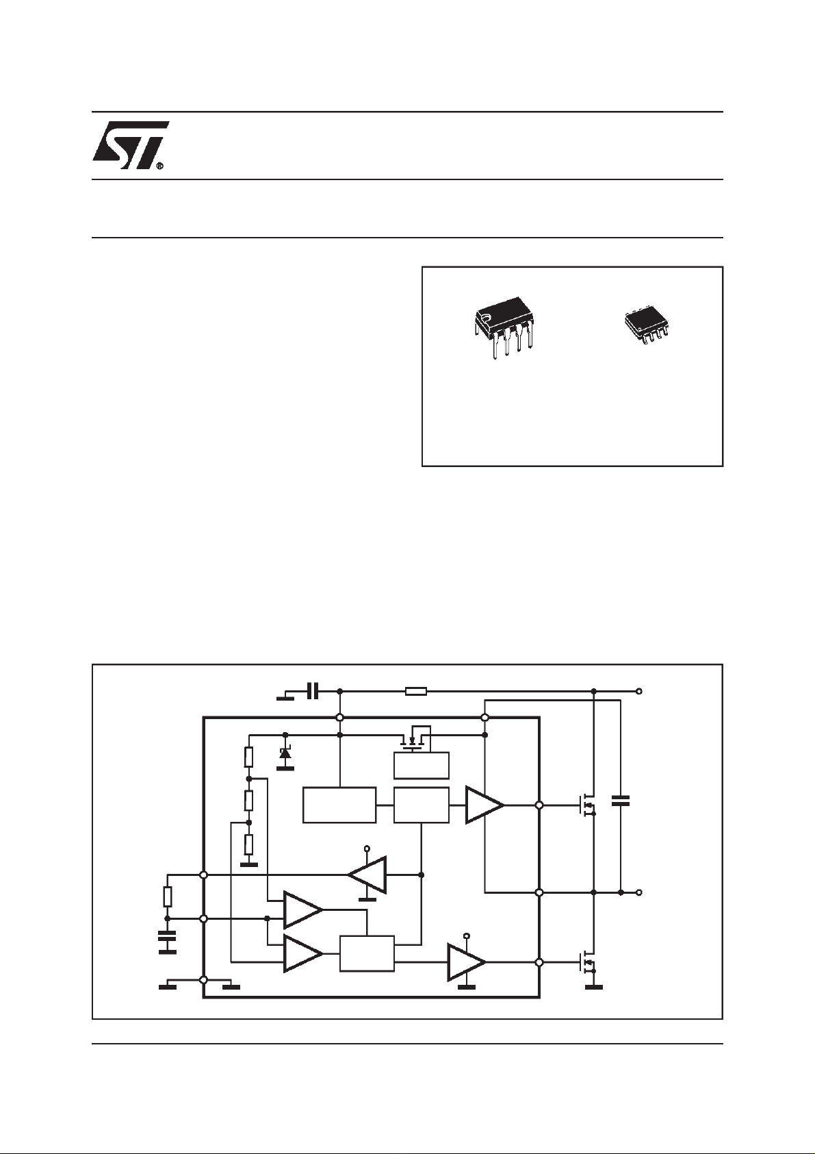
DESCRIPTION
The device is a high voltage half bridge driver with
built in oscillator. The frequency of the oscillator can
L6569
L6569A
HIGH VOLTAGE HALF BRIDGE
DRIVER WITH OSCILLATOR
Minidip SO8
ORDERING NUMBERS:
L6569 L6569D
L6569A L6569AD
be programmed using external resistor and capacitor. The internal circuitry of the device allows it to be
driven also by external logic signal.
The output drivers are designed to drive external nchannel power MOSFET and IGBT. Theinternal log-
µ
ic assures a dead time [typ. 1.25
conduction of the power devices.
Two version are available: L6569 and L6569A. They
differ in the low voltage gate driver start up sequence.
s] to avoid cross-
BLOCK DIAGRAM
R
C
VS
REGULATOR
2
F
R
F
C
3
F
C
F
GND
BUFFERR
COMP
COMP
S
18
Source
BIAS
V
S
LOGIC
June 2000
This ispreliminary information ona new product now in development. Details are subject to change without notice.
HV
CHARGE
PUMP
LEVEL
SHIFTER
BOOTV
HVG
7
HIGH
SIDE
DRIVER
OUT
6
V
S
LOW SIDE
DRIVER
LVG
54
D94IN058D
C
BOOT
H.V.
LOAD
1/13
L6569 L6569A
ABSOLUTEMAXIMUM RATINGS
Symbol Parameter Value Unit
(*) Supply Current 25 mA
I
S
V
CF
V
LVG
V
OUT
V
HVG
V
BOOT
V
BOOT/OUT
dV
BOOT
dV
OUT
T
stg
T
T
amb
(*)The device has an internal zener clamp between GND and VS (typical 15.6V).Therefore the circuit should not be driven by a DC low im-
pedance power source.
Note:
ESD immunity for pins 6, 7 and 8 is guaranteed up to 900 V (Human Body Model)
Oscillator Resistor Voltage 18 V
Low Side Switch Gate Output 14.6 V
High Side Switch Source Output -1 toV
High Side Switch Gate Output -1 to V
-18 V
BOOT
BOOT
Floating Supply Voltage 618 V
Floating Supply vs OUT Voltage 18 V
/dt VBOOT Slew Rate (Repetitive)
50 V/ns
±
/dt VOUT Slew Rate (Repetitive) ± 50 V/ns
Storage Temperature -40 to 150 °C
Junction Temperature -40 to 150 °C
j
Ambient Temperature (Operative) -40 to 125 °C
V
THERMAL DATA
Symbol Parameter Minidip SO8 Unit
R
th j-amb
Thermal Resistance Junction-Ambient Max 100 150 °C/W
RECOMMENDED OPERATINGCONDITIONS
Symbol Parameter Min. Max. Unit
Supply Voltage 10 V
CL
Floating Supply Voltage - 500 V
High Side Switch Source Output -1 V
BOOT-VCL
Oscillation Frequency 200 kHz
V
BOOT
V
V
S
OUT
f
out
PIN CONNECTION
V
RF
C
GND
S
F
1
2
3
4 LVG
7
6
5
BOOT8
HVG
OUT
V
V
2/13
D94IN059
PIN FUNCTION
N° Pin Description
1 VS Supply input voltage with internal clamp [typ.15.6V]
L6569 L6569A
2 RF Oscillator timing resistor pin.
A buffer set alternatively to V
and GND can provide current to the external resistor RF
S
connected between pin 2 and 3.
Alternatively, the signal on pin 2 can be used also to driveanother IC (i.e. another L6569 to drive
a full H-bridge)
3 CF Oscillator timing capacitor pin.
A capacitor connected between this pin and GND fixes (together with R
) the oscillating
F
frequency
Alternatively an external logic signal can be applied to the pin to drive the IC.
4 GND Ground
5 LVG Low side driver output.
The output stage can deliver 170mA source and 270mA sink [typ.values].
6 OUT Upper driver floating reference
7 HVG High side driver output.
The output stage can deliver 170mA source and 270mA sink [typ.values].
8 BOOT Bootstrap voltage supply.
It is theupper driver floating supply. The bootstrap capacitor connected between this pin and pin
6 can be fed by an internal structure named “bootstrap driver” (a patented structure). This
structure can replace the external bootstrap diode.
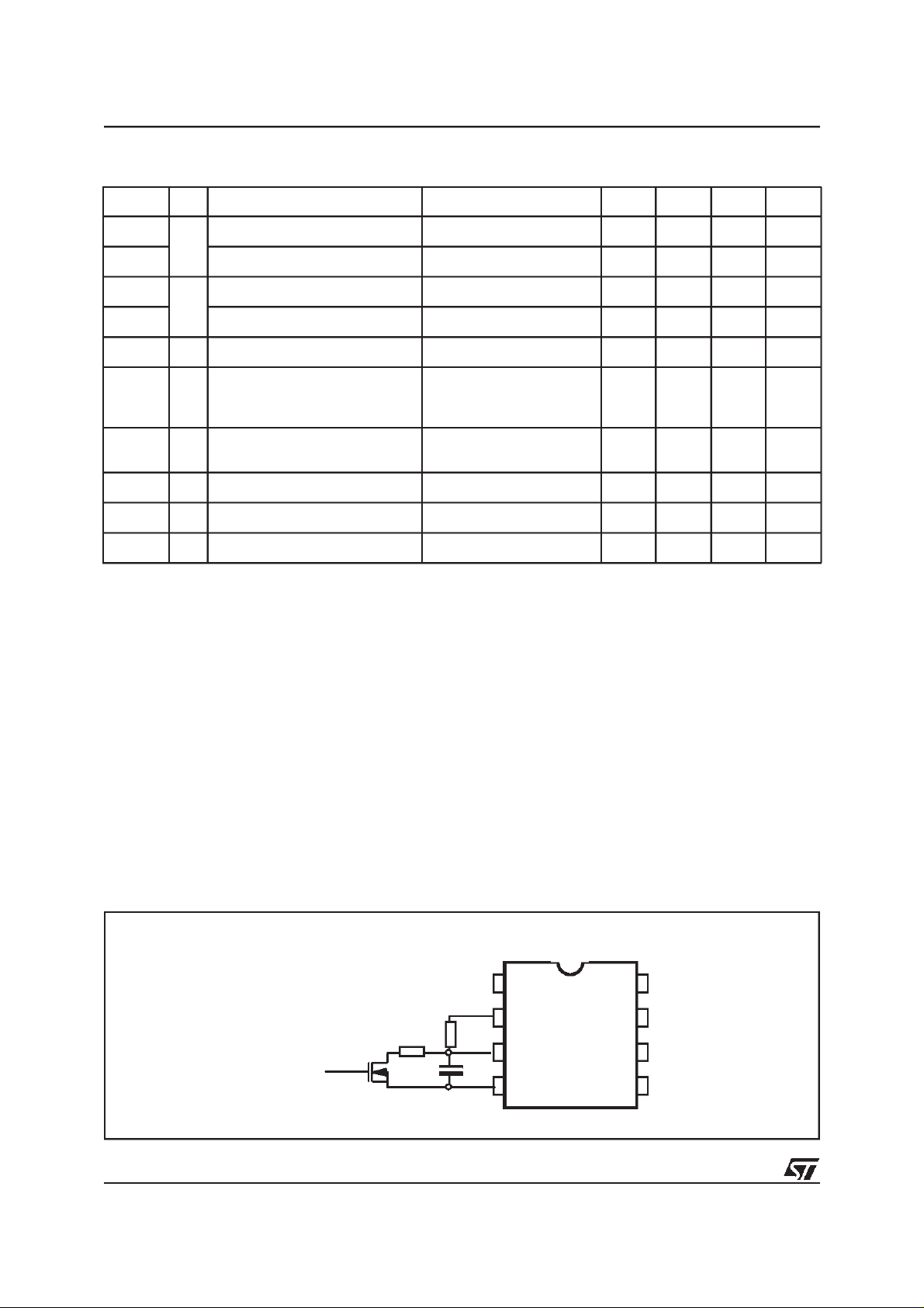
ELECTRICAL CHARACTERISTCS
(VS=12V;V
BOOT-VOUT
=12V;Tj=25°C; unless otherwise specified.)
Symbol Pin Parameter Test Condition Min. Typ. Max. Unit
V
SUVP
V
SUVN
V
SUVH
V
CL
I
SU
I
q
I
BOOTLK
1 VS TurnOn Threshold 8.3 9 9.7 V
VS TurnOffThreshold 7.3 8 8.7 V
VS Hysteresis 0.7 1 1.3 V
VS Clamping Voltage IS= 5mA 14.6 15.6 16.6 V
Start Up Current VS<V
Quiescent Current VS>V
8 Leakage Current BOOT pin vs
GND
I
OUTLK
6 Leakage Current OUT pin vs
GND
I
HVGSO
I
HVG SI
I
LVG SO
I
LVG S
7 High Side Driver Source Current V
High Side Driver Sink Current V
5 Low Side Driver Source Current V
I Low Side Driver SinkCurrent V
SUVN
SUVP
V
= 580V 5
BOOT
V
= 562V 5
OUT
= 6V 110 175 mA
HVG
= 6V 190 275 mA
HVG
= 6V 110 175 mA
LVG
= 6V 190 275 mA
LVG
150 250
500 700
A
µ
A
µ
A
µ
A
µ
3/13
L6569 L6569A
ELECTRICAL CHARACTERISTCS (continued)
Symbol Pin Parameter Test Condition Min. Typ. Max. Unit
V
N 2 RF High Level Output Voltage IRF=1mA V
RFO
-0.05 V
S
-0.2 V
S
V
RF OFF
V
CFU
V
CFL
t
d
DC Duty Cycle, Ratio Between Dead
R
ON
V
BC
I
AVE
f
out
RF Low Level Output Voltage IRF= -1mA 50 200 mV
3 CF Upper Threshold 7.7 8 8.2 V
CF Lower Threshold 3.80 4 4.3 V
Internal Dead Time 0.85 1.25 1.65
0.45 0.5 0.55
Time + Conduction Time of High
Side and Low Side Drivers
On resistance of Boostrap
LDMOS
Boostrap Voltage before UVLO VS= 8.2 2.5 3.6 V
1 Average Current from Vs No Load, fs = 60KHz 1.2 1.5 mA
6 Oscillation Frequency RT= 12K; CT= 1nF 57 60 63 kHz
120
OSCILLATORFREQUENCY
The frequency of the internal oscillator can be programmed using external resistor and capacitor.
The nominal oscillator frequency can be calculated using the following equation:
f
OSC
------------- ------- ---------------------
2RFCFIn2
1
⋅⋅⋅
------------- --------- ------------------ --==
1.3863 RFC
1
⋅⋅
F
s
µ
Ω
Where R
and CFare the external resistor and capacitor.
F
The device can be driven in ”shut down” condition keeping the C
taken:
1. When C
2. The forced discharge of the oscillator capacitor C
is to GND the high side driver is off and the low side is on
F
must not be shorter than 1us: a simple way to do this is to
F
limit the current discharge with a resistive path imposing R · C
Figure 1.
F
R
F
fault signal
R
C
GNDM
4/13
pin close to GND, but some cares have to be
F
>1µs (see fig.1)
F
1
2
3
4
8
7
6
5

L6569 L6569A
BootstrapFunction
The L6569 has an internal Bootstrap structure that enables the user to avoid the external diode needed, in similar devices, to perform the charge of the bootstrap capacitor that, in turns, provide an appropriate driving to the
Upper External Mosfet.
The operation is achieved with an unique structure (patented) that uses a High Voltage Lateral DMOS driven
by an internal charge pump (see Block Diagram) and synchronized, with a 50 nsec delay, with the Low Side
Gate driver (LVG pin), actually working as a synchronous rectifier .
The charging path for the Bootstrap capacitor isclosed via the Lower External Mosfet that is drivenON (i.e.LVG
High) for a time interval:
T
C=RF·CF
starting from the time the Supply Voltage VShas reached the Turn On Voltage (V
After time T
(see waveform Diagram) the LDMOSthatchargesthe Bootstrap Capacitor, is on with a RON=120Ω
1
(typical value).
In the L6569A a different start up procedure is followed (see waveform Diagram). The Lower External Mosfet is
driveOFF until V
hasreached the TurnOn Threshold(V
S
Being the LDMOS used to implement the bootstrap operation a ”bi-directional” switch the current flowing into
the BOOT pin (pin 8) can lead an undue stress to the LDMOS itself if a ZERO VOLTAGE SWITCHING operations is not ensured, and then an high voltage is applied to the BOOT pin. This condition can occur, for example,
when the load is removed and an high resistive value is placed in series with the gate of the external Power
Mos. To help the user to secure his design a SAFE OPERATING AREA for the Bootstrap LDMOS is provided
(fig. 7).
Let’s consider the steps that should be taken.
1) Calculate the Turn on delay ( td ) of your Lower Power MOS:
· In2 → 1.1 · RF·C
), then againthe TCtimeinterval starts asabove.
SUVPp
F
= 9 V typical value).
SUVP
d
id
+
=
t
RgR
()C
⋅⋅
iss
1
------------- ------ -ln
V
TH
-----------–
1
V
S
2) Calculate the Fall time ( tf ) of your Lower Power MOS:
R
R
+
g
-------------- -------- -- Q
=
t
f
VSV
id
⋅
TH
gd
–
where:
= External gate resistor
R
g
R
=50Ω, typical equivalent output resistance of the driving buffer (when sourcing current)
id
V
TH,Ciss
V
S
and Qgdare Power MOS parameters
= Low Voltage Supply.
3) Sketch the VBOOT waveform (using log-log scales) starting from the Drain Voltage of the Lower Power MOS
(remember to add the Vs, your Low Voltage Supply, value) on the Bootstrap LDMOS SOA . On fig. 8 an example
is given where:
= Low Voltage Supply
V
S
= High Voltage Supply Rail
V
HV
The V
voltage swing must fall below the curve identified by the actual operating frequency of your applica-
BOOT
tion.
5/13

L6569 L6569A
DEMOBOARD
To allow an easy evaluation of the device, a P.C. board dedicated to lamp ballast application has been designed.
Fig.11 shows the electrical schematic of a typical ballast application, while the PC and component layout isgiven in Fig12.This application has been designed to work with both the 110+/-20%V and the 220 +/- 20%V mains
by means of a voltage doubler configuration at the bulk capacitor. The ballast inductance and the operating frequency are especially designed for a 18 W Sylvania De-luxe T/E type bulb. The PTC for preheat at the start up
and the two back to back synchronization diodes, makes this application easy to implement and safe in operation.
part value
R1 15ohm 1W
R2, R3 22 ohm
R4 27K
R5 100K 1/2W
R6 47ohm
R7, R9 180K
R8 120K 1/2W
D1 18V zener
D2, D3 BYW100-100
D4,D5,D6,D7 1N4007
D8 1N4148
C1 560pF 50V
C2,C5 47µF 250V
C3 4.7µF 25V
C4 100nF 50V
C6 100nF 250V
C7-C8 8.2nF 630V
C9 470pF 630V
RV1 PTC 150ohm
Q1, Q2 STD2NB50-1
L1 2.4mH
6/13

Figure 2. Waveforms (L6569)
V
S
V
BOOT-VOUT
L6569 L6569A
V
SUVP
V
S
V
CF
LVG
Figure 3. Waveforms (L6569A)
V
S
V
BOOT-VOUT
τ=Ron*C
BOOT
T1
T
C
4.6V(typ)
D95IN250B
V
SUVP
V
S
V
CF
LVG
4.6V(typ)
τ=Ron*C
BOOT
T1
T
C
D95IN251B
7/13

L6569 L6569A
Figure 4. Typical Dead Time vs. Temperature
Dependency
Dead time [µsec]
1.7
1.6
1.5
1.4
1.3
1.2
1.1
1
0.9
-50 0 50 100 150
Temperature [C]
D96IN378A
Figure 5. Typical Frequency vs Temperature
Dependency
Frequency [KHz]
65
64
63
62
61
60
59
58
57
56
55
-50 -25 0 25 50 75 100 125
Temperature [C]
D96IN379A
Figure 6. Typical and Theoretical Oscillator
Frequency vs Resistor Value
f (KHz)
150
100
90
80
70
60
50
C=1nF
C=560pF
C=330pF
D96IN380
Theoretical
Figure 7. V
pin SOA for different Operating
boot
Frequency @ Tj=125°C
VBOOT
(V)
500
300
200
100
50
30
20
10
20 50 100 200 500 1,000 2,000 5,000 10,000
Figure 8. V
VBOOT
(V)
500
V
HV+VS
300
200
100
50
30
20
t
d
10
20 50 100 200 500 1,000 2,000 5,000 10,000
110KHz
70KHz
50KHz
20KHz
150KHz
Time (ns),from LVG Transition High
pin SOA @ Tj= 125°C
boot
ACTUAL OPERTATING
FREQUENCY
VBOOT
t
f
Time (ns),from LVG Transition High
V
S
D96IN381
D96IN416
Figure 9. Typical Rise and Fall Times vs. Load
Capacitance
time [nsec]
300
250
200
150
100
D96IN417
Tr
Tf
8/13
30
20
5678910 15 20 30 4050
Resistor Value (Kohm)
50
0
0123456
C [nF]
For both high and low side buffers @25°C Tamb

Figure 10. Quiescent Current vs. Supply Voltage.
L6569 L6569A
Iq (µA)
4
10
3
10
2
10
D96IN418
10
02468101214VS(V)
Figure 11. CFL Demoboard 110/220V Inputs.
4 x1N4006
220V
N
110V
R8
120K
1/2W
D7 D4
D5D6
R1 15 1W
L1=2.4mH core THLCC E2006-B4 Ref also VOGH 5750409200 2.4mH
C7-C8=PS8n2J H3 630-2ATH
C5
47µ
250V
C2
47µ
F
250V
R5 100K
1/2W
C3
F
4.7µ
25V
R4
27K
1/4W
D8
1N4148
F
ZPD 18V
V
S
RF
L6569
CF
C1
560pF
50V
D1
C9 470pF630V
R6 471/4W
BOOT
HVG
OUT
LVG
GND
C4100nF 50V
R2 22 1/4W
R3 22 1/4W
D96IN419B
R10 10K
1/4W
Q1
STD2NB50-1
Q2
STD2NB50-1
180K
1/4W
BYW100-100
D2
D3 BYW100-100
R9
180K
1/4W
R7
C6
100nF
250V
L1=2.4mH
C7
8.2nF
630V
C8
8.2nF
630V
CFL
SYLVANIA DELUXT/E18W
LAMP
RV1
PTC 150
350V
9/13

L6569 L6569A
Figure 12. PC Board and Components Layout.
Component Side
Copper Side
10/13

L6569 L6569A
DIM.
D (1) 4.8 5.0 0.189 0.197
F (1) 3.8 4.0 0.15 0.157
(1) D and F donot include mold flash or protrusions. Mold flashor
MIN. TYP. MAX. MIN. TYP. MAX.
A 1.75 0.069
a1 0.1 0.25 0.004 0.010
a2 1.65
a3 0.65 0.85 0.026 0.033
b 0.35 0.48 0.014 0.019
b1 0.19 0.25 0.007 0.010
C 0.25 0.5 0.010 0.020
c1 45° (typ.)
E 5.8 6.2 0.228 0.244
e 1.27 0.050
e3 3.81 0.150
L 0.4 1.27 0.016 0.050
M 0.6 0.024
S8°(max.)
potrusions shall not exceed 0.15mm (.006inch).
mm inch
0.065
OUTLINE AND
MECHANICAL DATA
SO8
11/13

L6569 L6569A
DIM.
MIN. TYP. MAX. MIN. TYP. MAX.
A 3.32 0.131
a1 0.51 0.020
B 1.15 1.65 0.045 0.065
b 0.356 0.55 0.014 0.022
b1 0.204 0.304 0.008 0.012
D 10.92 0.430
E 7.95 9.75 0.313 0.384
e 2.54 0.100
e3 7.62 0.300
e4 7.62 0.300
F 6.6 0.260
I 5.08 0.200
L 3.18 3.81 0.125 0.150
Z 1.52 0.060
mm inch
OUTLINE AND
MECHANICAL DATA
Minidip
12/13

L6569 L6569A
Information furnished isbelieved to be accurate and reliable. However, STMicroelectronics assumes no responsibility for the consequences
of useof suchinformation nor for any infringement of patents or otherrightsofthird parties whichmay result from its use.No license is granted
by implicationor otherwise under any patent or patent rights of STMicroelectronics. Specifications mentioned in this publication are subject
to change without notice. This publication supersedes and replaces all information previously supplied. STMicroelectronics products are not
authorized for use as critical components in life support devices or systems without express written approval of STMicroelectronics.
The ST logo is a registered trademark of STMicroelectronics
2000 STMicroelectronics - All Rights Reserved
Australia - Brazil - China - Finland - France - Germany - Hong Kong - India- Italy - Japan - Malaysia -Malta- Morocco - Singapore - Spain
STMicroelectronics GROUP OF COMPANIES
- Sweden - Switzerland - United Kingdom - U.S.A.
http://www.st.com
13/13
 Loading...