

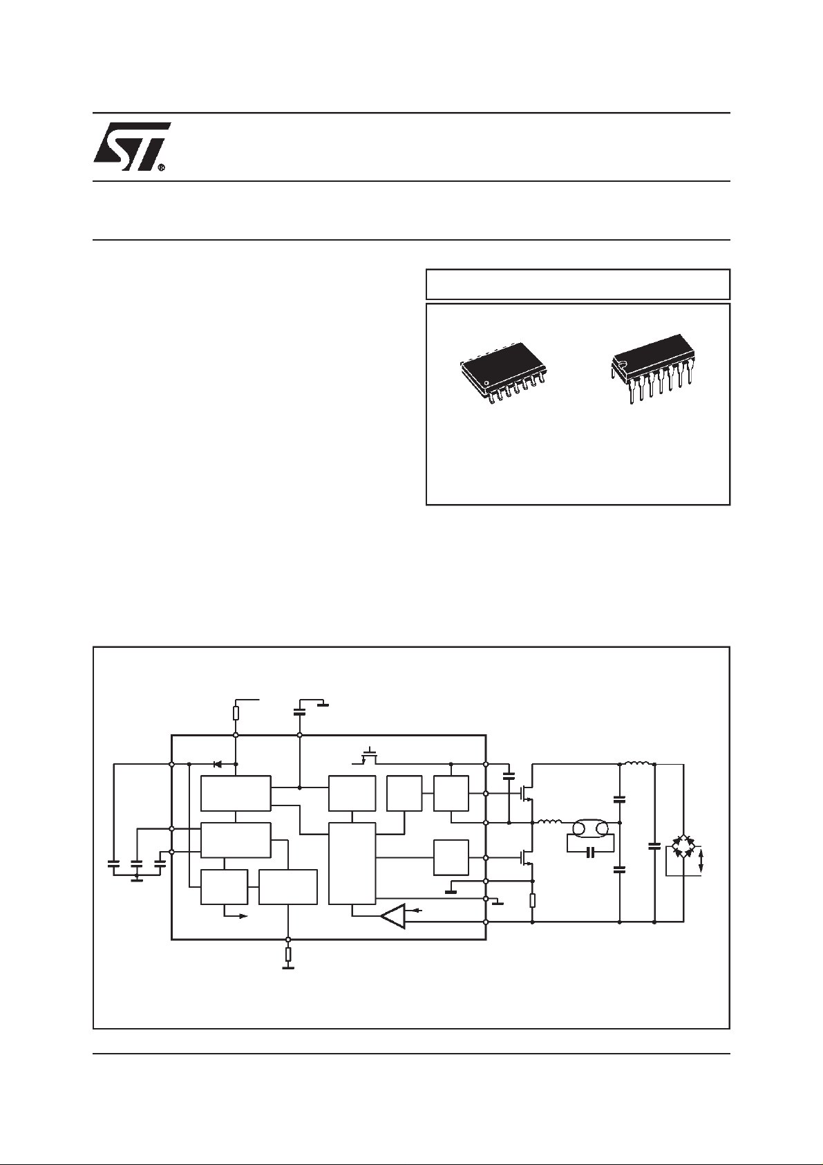
HIGH VOLTAGE DRIVER FOR CFL
n
BCD-OFF LINE TECHNOLOGY
n FLOATING SUPPLY VOLTAGE UP TO 570V
n
GND REFERRED SUPPLY VOLTAGE UP TO
18V
n UNDER VOLTAGE LOCK OUT
n
CLAMPING ON Vs
n
DRIVER CURRENT CAPABILITY:
30mA SOURCE
70mA SINK
n
PREHEAT AND FREQUENCY SHIFT TIMING
DESCRIPTION
The device is amonolithic high voltage integrated circuit designed to drive CFL and small TL lamps with a
minimum part count.
It provides all the necessary functions for proper preheat, ignition andsteady state operation of the lamp:
♦ variable frequency oscillator;
L6567
MULTIPOWER BCD TECHNOLOGY
SO14 DIP14
ORDERING NUMBERS:
L6567D L6567
♦
settable preheating and ignition time;
♦
capacitive mode protection;
♦
lamp power independentfrom mains voltage variation.
Besides the control functions, theIC provides the level shift anddrive function for twoexternal power MOS
FETs in a half-bridge topology.
BLOCK DIAGRAM
V
5
S
CF
12
CI
14
C
SCfCi
RHV
FEED FORWARD
VCO +
FREQ. SHIFTING
VOLTAGE
REFERENCE
Rhv
13
comp.
to
Vhv
BIAS
CURRENT
GENERATOR
Ref
Cp/Cav
CP
8
F
1
V
S
PREHEATING
TIMING
LOGIC
10
R
REF
LEVEL
SHIFTING
C
HIGH
SIDE
DRIVER
LOW
SIDE
DRIVER
S
Cboot
G1
2
S1
3
6
G2
7
PGND
SGND
11
9
R
S
T1
L
T2
Rshunt
D96IN441B
Vhv
Lamp
CL
Chv
Chv
MAINS
January 2000
This ispreliminary information on a new product now in development. Details are subject to change without notice.
1/15
L6567
PIN FUNCTION
N° Pin Description
1F
2 G1 Gate of high side switch
3 S1 Source of high side switch
4 NC High Voltage Spacer. (Should be not connected)
5V
6 G2 Gate of low side switch
7 PGND Power Ground
8 CP First timing (TPRETIGN), then averaging the ripple in the representation of the HVB (derived
9R
10 R
11 SGND Signal Ground. Internally Connected to PGND
12 CF Frequency setting capacitor
13 RHV Start-up supply resistor, then supply voltage sensing.
14 CI Timing capacitor for frequency shift
Floating Supply of high side driver
S
Supply Voltage for GND level control and drive
S
through RHV).
R
S
Reference resistor for current setting
REF
: current monitoring input
SHUNT
PIN CONNECTION (Top view)
2/15
FS
G1
S1
N.C.
V
G2
PGND
14
2
3
4
S
5
6
7
D96IN440
13
12
11
10
9
8
CI1
RHV
CF
SGND
RREF
RS
CP

ABSOLUTEMAXIMUM RATINGS
Symbol Parameter Value Unit
L6567
Low Voltage Supply 18 (1) V
S
Mains Voltage Sensing VS +2VBE (2)
Preheat/Averaging 5 V
Oscillator Capacitor Voltage 5 V
Frequency Shift Capacitor Voltage 5 V
Reference Resistor Voltage 5 V
Current Sense Input Voltage -5 to 5 V
V
V
V
V
V
V
RHV
CP
CF
V
CI
RREF
RS
transient 50ns -15 V
V
G2
V
S1
Low Side Switch Gate Output 18 V
High Side Switch Source Output: normal operation -1 to 373 V
0.5sec mains transient -1 to 550 V
VG1 High Side Switch Gate Output: normal operation -1 to 391 V
0.5sec mains transient -1 to 568 V
with respect to pin S1 V
V
FS
Floating Supply Voltage: normal operation 391 V
be
to V
S
0.5sec mains transient 568 V
V
V
FS/S1
∆V
FS/∆T
∆V
S1/∆T
I
RHV
I
Vs
T
stg
T
NOTES: (1) Do not exceed package thermal dissipation limits
Note: ESD immunity for pins 1, 2 and 3 is guaranteed up to 900 V (Human Body Model)
Floating Supply vs S1 Voltage 18 V
VFS Slew Rate (Repetitive) -4 to 4 V/ns
VS1 Slew Rate (Repetitive) -4 to 4 V/ns
Current Into R
Clamped Current into V
HV
S
Storage Temperature -40 to 150 °C
Junction Temperature -40 to 150 °C
j
(2) For VS ≤ VShigh 1
(3) For VS > VS high 1
(4) Internally Limited
3 (3) mA
200 (4) mA
3/15
L6567
ELECTRICAL CHARACTERISTCS
(VS=12V;R
Symbol Parameter Test Condition Min. Typ. Max. Unit
- SUPPLYVOLTAGE SECTION
V
S
=30KΩ;CF= 100pF; Tj=25°C; unless otherwise specified.)
REF
V
S high 1
V
S high2
V
S low 2
V
S HYST
V
S low 1
I
SSP
I
SOP
VSTurn On Threshold 10.7 11.7 12.7 V
VSClamping Voltage VS = 20mA 12 13 14 V
VSTurn Off Threshold 9 10 11 V
Supply Voltage Hysteresis 1.5 1.65 1.8 V
VSVoltage to Guarantee
=”0”and VG2=”1
V
G1
16V
VSSupply Current at Start Up VS= 10.6V Before turn on 50 250 mA
VSSupply Operative Current VS= VShigh 1 1.2 mA
OSCILLATOR SECTION
f
osc min
f
osc 600
f
osc 1mA
Minimum Oscillator frequency I
Feed Forward Frequency I
m
Feed Forward Frequency I
= 0mA; CI = 5V 41.7 43 44.29 kHz
RHV
= 600mA 47.88 50.4 52.92 kHz
RHV
= 1mA 79.8 84 88.2 kHz
RHV
fosc max Maximum Oscillator Frequency CI = 0V 96.75 107.5 118.25 KHz
∆ICF/∆V
Oscillator Transconductance 9 17.5 µA/V
CI
PREHEAT/IGNITION SECTION
P.H.T. Preheat Time Cp = 150nF 0.88 1 1.12 sec
P.H.clocks Number of Preheat Clocks 16
IGN.clocks Number of Ignition Clocks 15
RATE OF FREQUENCY CHANGE SECTION
ICIP charge CI Charging Current During
106 118 130 mA
Preheat
ICII charge CI Charging Current During
1 1.2 1.4 mA
Ignition
ICI disch CI Discharge Current -52 -47 -42 mA
V
TH CI
CI Low Voltage Threshold 10 100 mV
RS - THRESHOLD SECTION
V
CMTH
Capacitive Mode Voltage
02040mV
Threshold
V
PH
Preheat Voltage Threshold -0.64 -0.6 -0.56 V
G1 - G2DELAY TIMES SECTION
G1
DON
On Delay of G1 Output 1.05 1.4 1.75
4/15
s
µ
L6567
ELECTRICAL CHARACTERISTCS
(Continued)
Symbol Parameter Test Condition Min. Typ. Max. Unit
G2
DON
G1
+
DONG1ON
------- ------ -------- ------- -------- --- -- --
G2
+
DONG2ON
On Delay of G2 Output 1.05 1.4 1.75
Ratio between Delay Time +
Conduction Time of G1 and G2
I
= 1mA; Cl = 5V
RHV
Cl = 0V
0.87
0.77
1.15
1.30
LOW SIDE DRIVER SECTION
Ron G2 so G2 Source Output Resistance V
Ron G2 si G2 Sink OutputResistance V
Ron G1 so G1 Source Output Resistance V
Ron G1 si G1 Sink OutputResistance V
= 12V,V = 3V 80 190
S
= 12V,V = 3V 65 125 Ω
S
= 10V,V = 3V 80 190 Ω
S
= 10V,V = 3V 65 125 Ω
S
HIGH SIDE DRIVER SECTION
I
FSLK
I
S1 LK
Leakage Current of FS PIN to
GND
Leakage Current of S1 PIN to
GND
VFS= 568V; G1 = L
= 568V; G1 = H
V
FS
VS1= 568V; G1 = L
= 568V; G1 = H
V
S1
5
5
5
5
BOOTSTRAP SECTION
Boot Th BOOTSTRAP Threshold V
= 10.6V before turnon 5 (*) V
S
µ
Ω
µA
µA
µA
µA
s
AVERAGE RESISTOR
R
AVERAGE
(*) Beforestartingthe first commutation; when switching 6V is guaranteed.
Average Resistor 27 38.5 50 kΩ
General operation
The L6567 uses a small amount of current from a supply resistor(s) to start the operation of the IC. Once start
up condition isachieved, the IC turns on the lower MOS transistor of the half bridge which allows the bootstrap
capacitor to charge. Once this is achieved, the oscillator begins toturn on the upper and lower MOStransistors
at high frequency, and immediately ramps down to a preheat frequency. During this stage, the IC preheats the
lamp and after a predetermined time ramps down again until it reaches the final operating frequency. The IC
monitors thecurrentto determine if the circuitisoperating in capacitivemode.If capacitive switchingis detected,
the IC increases the output frequency until zero-voltage switching is resumed.
Startup and supply in normal operation
At start up the L6567 is powered via a resistor connected to the RHVpin (pin 13) from the rectified mains. The
current charges the C
V
SLOW1
(max 6V), the low side MOS transistor is turned on while the high side one is kept off. This condition
assures that the bootstrap capacitor is charged. When V
the R
pin does not provide anymore the supply current for the IC (seefig.1).
HV
capacitor connected to the VSpin (pin 5). When the VSvoltage reaches the threshold
S
SHIGH1
threshold is reached the oscillator starts, and
5/15

L6567
Figure 1. Start up
VSHIGH1
VSLOW1
TDT
G
V
lowside mosfet
VS
0
0
VG-VS
high side mosfet
0
CF
0
TIME
Oscillator
The circuit starts oscillating when the voltage supply VShas reached the V
condition theoscillatorcapacitor C
ly by the external resistor R
and resistor R
. This fixed value is called F
REF
REF
(at pin12) ischarged and discharged symmetrically with a current setmain-
F
connected to pin 10. The value of the frequency is determined by capacitor C
. A dead time TDTbetween the ON phases of the transistors
MIN
S HIGH1
threshold. In steady state
is provided for avoiding cross conduction, so the duty cycle for each is less than 50%. The dead time depends
on R
The IC oscillating frequency is between F
value (fig. 7).
REF
MIN
and F
MAX
= 2.5 · F
in all conditions.
MIN
F
Preheatingmode
The oscillator starts switching at the maximum frequency F
. Then the frequency decreases at once to reach
MAX
the programmed preheating frequency (fig.2). The rate of decreasing (df/dt) is determined by the external capacitor C
current is adjusted by sense resistance R
sense resistor R
(pin 14). The preheat time T
I
(connected between pin 9-RS- and pin 7-PGND-). At pin 9 the voltage drop on R
SHUNT
is adjustable with external components (R
PRE
. During the preheating time the load current is sensed withthe
SHUNT
and CP). The preheat
REF
SHUNT
is sensed at the moment the lowside MOS FET is turned off. There is an internal comparator with afixed threshold V
old is reached, the frequency is held constant for the programmed preheating time T
T
current that depends on R
So the preheat mode is programmable with external components as far as T
as far as the preheating current is concerned (choosing properly R
Land C
The circuit is held in the preheating mode when pin 8 (C
In case F
the low side MOS transistor gate on and the high side gate off. This condition is kept until VSundershoots V
6/15
:ifVRS>VPHthe frequency is decreased and ifVRS<VPHthefrequency is increased. Ifthe VPHthresh-
PH
is determined by the external capacitor CP(pin8) and by the resistor R
PRE
).
L
is reached during preheat, the IC assumes an open load. Consequently the oscillation stops with
MIN
, and these 16 cycles determine the T
REF
) is grounded.
P
REF:CP
.
PRE
is concerned (R
PRE
and the resonant load components:
SHUNT
.
PRE
is charged 16 times with a
REF&CP
SLOW1
) and
.

L6567
Figure 2. Preheating and ignition state.
FREQUENCY
FMAX
MIN
F
preheating
state
ignition
state
burning state
TIME
Ignitionmode
At the end of the preheat phasethe frequency decreses tothe minimumfrequency (F
coil current and a high voltage appearing across the lamp. That is because the circuit works near resonance.
This high voltage normally ignites the lamp. There is no protection to avoid high ignition currents through the
MOS transistors when thelampdoesn’t ignite. This only occurs inan end of lamp life situation in which the circuit
may break. Now the lowest frequency is the resonance frequency of L and C
The ignition phase finishes when the frequency reaches F
elapsed. The ignition timeis related toT
the same current used to charge it during T
PRE:TIGN
PRE
The frequency shiftingslope is determined by C
During the ignition time the V
monitoring function changes inthe capacitive mode protection.
RS
= (15/16) · T
.
.
I
or (at maximum) when the ignition time has
MIN
. The CPcapacitor is charged 15times with
PRE
(the capacitor across the lamp).
L
), causing anincreased
MIN
Steady state operation: feed forwardfrequency
The lamp starts operating at F
, determined by R
MIN
and CFdirectly after the ignition phase. To prevent too
REF
high lamp power at high mains voltages, a feed forward correction is implemented. At the end of the preheat
phase the R
increases and overcomes a value set by R
pinisconnected to an internal resistortosensethe HighVoltage Bus.Ifthe current in this resistor
HV
, the current that charges the oscillator capacitor CFincreases
REF
too. The effect is an increase in frequency limiting the power in the lamp. In order toprevent feed forward of the
ripple of the V
voltage, the ripple is filtered with capacitor CPon pin 8 and an integrated resistor R
HV
AVERAGE
Figure 3. Burn state
FREQUENCY
feed forward mode
MIN
F
Irhv
.
7/15

L6567
Capacitivemode protection
During ignition and steady state the operating frequency is higher than the resonance frequency of the load
(L,C
L,RLAMP
order to maintain Zero Voltage Switching.
If the operating frequency undershoots the resonance frequency ZVS doesn’t occur and causes hard switching
of theMOStransistors. The L6567 detects this situation by measuring V
on. At pin 9 there is an internal comparatorwith thresholdV
assumed and the frequency is increased as long as this situation is present. The shift is determined by CI.
Steady state frequency
At anytime during steadystate thefrequency isdetermined by the maximumon the following three frequencies:
and R
FILAMENT
), so the transistors are turned on during the conduction time of the body diode in
when the low side MOS FET is turned
RS
(typ~20mV): if VRS<V
CMTH
capacitive mode is
CMTH
f
STEADYSTATE
=MAX{F
MIN,fFEEDFORWARD,fCAPACI T IV EMODEPROT ECTIO N
}.
IC supply
At start up the IC is supplied with a current that flows through RHVand an internal diode to the VSpin whichcharges theexternal capacitor C
provide anymore the supply current. The easiest way to charge the C
. In steady state condition RHVis used as a mainsvoltage sensor, so it doesn’t
S
capacitor (and tosupply theIC)is to use
S
a charge pump from the middle point of the half bridge.
To guarantee a minimum gate power MOS drive, the IC stops oscillating when V
restart once the V
starts operating atf = F
will become higher than V
S
,then the frequency shifts towards F
MAX
. A minimum voltage hysteresis isguaranteed. The IC re-
SHIGH1
. The timing ofthis frequency shifting is T
MIN
is lower than V
S
SHIGH2
. It will
IGN
(that is: CPcapacitor is charged and discharged 15 times).Now the oscillator frequency is controlled as in standard burning condition (feedforward and capacitive mode control). Excess charge on C
nal clamp that turns on at voltage V
SCL
.
is drained by an inter-
S
Groundpins
Pin 7(PGND) is the ground reference of the IC with respect to the application. Pin 11( SGND) provides a local
signal ground reference for the components connected to the pins C
P,CI,RREF
and CF.
Relationship betweenexternal components and sistemworking condition
L6567 is designed todriveCFL and TLlamps with a minimumpartcount topology. This feature implies that each
external component isrelated to one or more circuit operating state.
This table is a short summary of these relationships:
F
---> R
MIN
F
FEEDFORWARD
T
PRE&TIGN
F
PRE
T
DT
df/dt ---> C
---> R
---> R
REF&CF
---> CF&I
---> CP&R
SHUNT
REF
I
RHV
REF
,L,CL, LAMP
Some useful formulas can wellapproximate the values:
1
MIN
≅
------------ -------- -------------
8R
⋅⋅
REFCF
F
If I
following expression:
8/15
is greater than: , the feed forward frequency is settledand the frequency value is fitted by the
RHV
I
RHV
≥
15
------------ --
R
REF
F
FE EDFO R W ARD
I
RHV
----------- --------- -≅
121 CF⋅

L6567
Other easy formulas fit rather well:
T
T
DT
PRE
≅
46.75 · 10
≅ 224 · C
^-12
·R
P·RREF
REF
As far asdf/dt isconcerned, there are no easyformulas that fitthe relation between CF,RF, and CI.CIis charged
and discharged by three different currents that are derived from different mirroringratios by thecurrent flowing
on R
. The voltage variations on CIare proportional to the current that charges CF, that is to say they are
REF
proportional to df/dt.
The values obtained in the testing conditions (C
= 100nF) are:
I
during preheating and workingconditions the typical frequency increase is ~ 20KHz/ms, the typical decrease is
~-10Khz/ms;
During ignition the frequency variation is ~ -200Hz/ms.
If slower variations are needed, CI has to be increased.
Due to these tight relationships, it is recommended to follow a precise procedure: first R
has to be chosen
HV
looking at startup current needs and dissipation problems. Then the feed forward frequency range has to be
determined, and so C
Given a certain C
The other external parameters (R
is set.
F
F,RREF
is set in order to fix F
SHUNT
and CI) can be chosen at the end because they are just related to a
. Now CPcan be chosed to set the desired T
MIN
PRE
and T
IGN
.
single circuit parameters.
9/15

L6567
Figure 4. IC Operation
START
PREHEATING MODE
N
OPEN LOADDETECTION:STOP
LOW SIDE MOSON
AND HIGH SIDEMOS OFF
F>F
MIN
Y
DECREASE
FREQUENCY
Y
Y
SHIGH2
PRE
PH
INCREASE
FREQUENCY
N
N
Y
V
S>VSLOW1
NO OSCILLATION
LOW SIDE MOS ON
HIGH SIDE MOS OFF
V
S>VSHIGH1
STARTOSCILLATION
F=F
MAX
T=T
0
N
V
>V
S
Y
T=T0+T
N
NY
VRS>V
STOP OSCILLATION
LOW SIDE MOS ON
HIGH SIDE MOS OFF
BURNING MODE
VS>V
N
IGNITION MODE
DECREASE
FREQUENCY
FEED FORWARDMODE
ACTIVATED
N
S>VSHIGH2
V
Y
VRS<VCMTH
N
Y
F>FFEEDFORWARD
SHIGH2
Y
T>T0+T
PRE+TIGN
Y
N
VRS<V
NY
F>F
MIN
Y
Y
N
CMTH
INCREASE
FREQUENCY
10/15
V
S>VSHIGH1
Y
RESTARTWITH
F=F
MAX
FREQUENCYSHIFTS IN T=T
TOWARDSBURNINGSTATECONDITION
(F=MAX{F
MAX,FFEEDFORWARD,FCAPACITIVEMODE
N
IGN
N
DECREASE
FREQUENCY
F>F
Y
MIN
INCREASE
FREQUENCY
})

L6567
Figure 5. Working frequency vs I
@R
160.00
150.00
140.00
130.00
120.00
110.00
100.00
90.00
80.00
70.00
frequen cy [kH z]
60.00
50.00
40.00
30.00
20.00
10.00
0.00
0.20 0.40 0.60 0.80 1.00 1.20
Figure 6. Frequency vs CF@R
160.00
150.00
140.00
130.00
120.00
110.00
100.00
90.00
80.0 0
70.00
frequency[kHz]
60.00
50.00
40.0 0
30.00
20.00
10.00
0.00
60.00 100.00 140.00 180.00 220.0040.00 80.00 120.00 160.00 200.00 240.00
Figure 7. TDTvs R
2.40
= 30Kohm
REF
Rref=30Kohm
Irhv [m A]
Cf [pF]
@CF= 100pF
REF
Tdt [calculated data]
REF
RHV
=30Kohm
Rref=30Kohm
Cf=47pF
Cf=56pF
Cf=68pF
Cf=82pF
Cf=100 pF
Cf=120pF
Cf=150pF
Cf=180pF
Cf=220pF
I=1mA
I=0 .75 mA )
I=0.5mA
Figure 8. Frequency vs I
120.00
100.00
80.00
Rref=20K
frequency [kHz]
Rref=22K
Rref= 24K
60.00
Rref=27K
Rref=30K
Rref= 33K
Rref=36K
40.00
Rref=39K,43K, 47K,51K
0.20 0.40 0.60 0.80 1.00 1.20
Figure 9. Frequency vs I
100.0 0
80.00
Rref=20K
Rref=22K
60.00
Rref=24K
frequency [kHz]
Rref=27K
Rref=30K
Rref=33K
40.00
Rref=36K
Rref=39K,43K
20.00
0.20 0.40 0.60 0.80 1.00 1.20
Irhv [mA]
Figure 10. Frequency vs I
80.0 0
@CF= 82pF
RHV
Irhv [m A ]
@CF=100pF
RHV
@CF=120pF
RHV
Tdt[measureddata]
2.00
1.60
Tdt [us]
1.20
0.80
20.00 30.00 40.00 50.00 6 0.00
Rref[Kohm]
60.0 0
Rref=20K
Rref=22K
Rref=24K
frequency [kHz]
40.0 0
Rref=27K
Rref=30K
Rref=33K
Rref=36K
Rref=39K
Rref=43K, 4 7K, 51K
20.0 0
0.20 0.40 0. 60 0.80 1. 00 1.20
Irhv [mA]
11/15

L6567
Figure 11. Frequency vs I
80.00
60.00
Rref=20K
40.00
frequency [kHz]
Figure 12. F
Rref=22K
Rref=24K
Rref= 27K
Rref= 30K
Rref= 33K
Rref=36K
Rref= 39K
20.00
Rref=43 K, 47K , 51 K
0.20 0.40 0.60 0.80 1.00 1.20
: measurementsand calculations
MIN
100.00
80.00
Irhv [m A ]
@CF= 150pF
RHV
measuraments
Fmin=1/(8*Cf*Rref)
Figure 13. F
Freq . fe ed forwa rd [H z]
120000.00
110000.00
100000.00
90000.00
80000.00
70000.00
60000.00
50000.00
40000.00
30000.00
20000.00
10000.00
calculations(1/121)*Irhv/Cf
0.00
0.40 0.60 0.80 1.00 1.20
FEED FORWARD
calculations
meas u rements
Irhv [mA]
: measurements and
Cf=8 2pF
Cf=1 00p F
Cf=120pF
Cf=1 50p F
60.00
Fmin [KHz]
40.00
20.00
0.00
20.00 30.00 40.00 50.00
Rref[Kohm]
Cf=82pF
Cf=100pF
Cf=120pF
Cf=150pF
12/15

L6567
DIM.
MIN. TYP. MAX. MIN. TYP. MAX.
a1 0.51 0.020
B 1.39 1.65 0.055 0.065
b 0.5 0.020
b1 0.25 0.010
D 20 0.787
E 8.5 0.335
e 2.54 0.100
e3 15.24 0.600
F 7.1 0.280
I 5.1 0.201
L 3.3 0.130
Z 1.27 2.54 0.050 0.100
mm inch
OUTLINE AND
MECHANICAL DATA
DIP14
13/15

L6567
DIM.
MIN.. TYP. MAX.. MIN.. TYP.. MAX..
A 1.75 0.069
a1 0.1 0.25 0.004 0.009
a2 1.6 0.063
b 0.35 0.46 0.014 0.018
b1 0.19 0.25 0.007 0.010
C 0.5 0.020
c1 45° (typ.)
D (1) 8.55 8.75 0.336 0.344
E 5.8 6.2 0.228 0.244
e 1.27 0.050
e3 7.62 0.300
F (1) 3.8 4 0.150 0.157
G 4.6 5.3 0.181 0.209
L 0.4 1.27 0.016 0.050
M 0.68 0.027
S8°
(1) D and F do not include mold flashor protrusions. Mold flash or
potrusions shall not exceed0.15mm (.006inch).
mm inch
(ma x.)
OUTLINE AND
MECHANICAL DATA
SO14
14/15

L6567
Information furnished is believed tobe accurate and reliable. However,STMicroelectronics assumes no responsibility for the consequences
of useof such information nor for any infringementof patents or other rightsof third partieswhich may result from its use. No license is granted
by implication or otherwise under any patent or patent rights of STMicroelectronics. Specifications mentioned in this publication are subject
to change without notice. This publication supersedes and replaces all information previously supplied. STMicroelectronics products arenot
authorized for use as critical components in life support devices or systems without express written approval of STMicroelectronics.
The ST logo is a registered trademark of STMicroelectronics
1999 STMicroelectronics - All Rights Reserved
Australia - Brazil - China - Finland - France - Germany - Hong Kong - India - Italy - Japan - Malaysia - Malta- Morocco - Singapore - Spain
STMicroelectronics GROUP OF COMPANIES
- Sweden- Switzerland - United Kingdom - U.S.A.
http://www.st.com
15/15
 Loading...