

ST L6566BH User Manual
Features
■ Selectable multimode operation: fixed
frequency or quasi-resonant
■ On-board 840 V high voltage startup
■ Advanced light load management
■ Low quiescent current (< 3 mA)
■ Adaptive UVLO
■ Line feedforward for constant power capability
vs. mains voltage
■ Pulse-by-pulse OCP, shutdown on overload
(latched or auto-restart)
■ Transformer saturation detection
■ Programmable frequency modulation for EMI
reduction
■ Latched or auto-restart OVP
■ Brownout protection
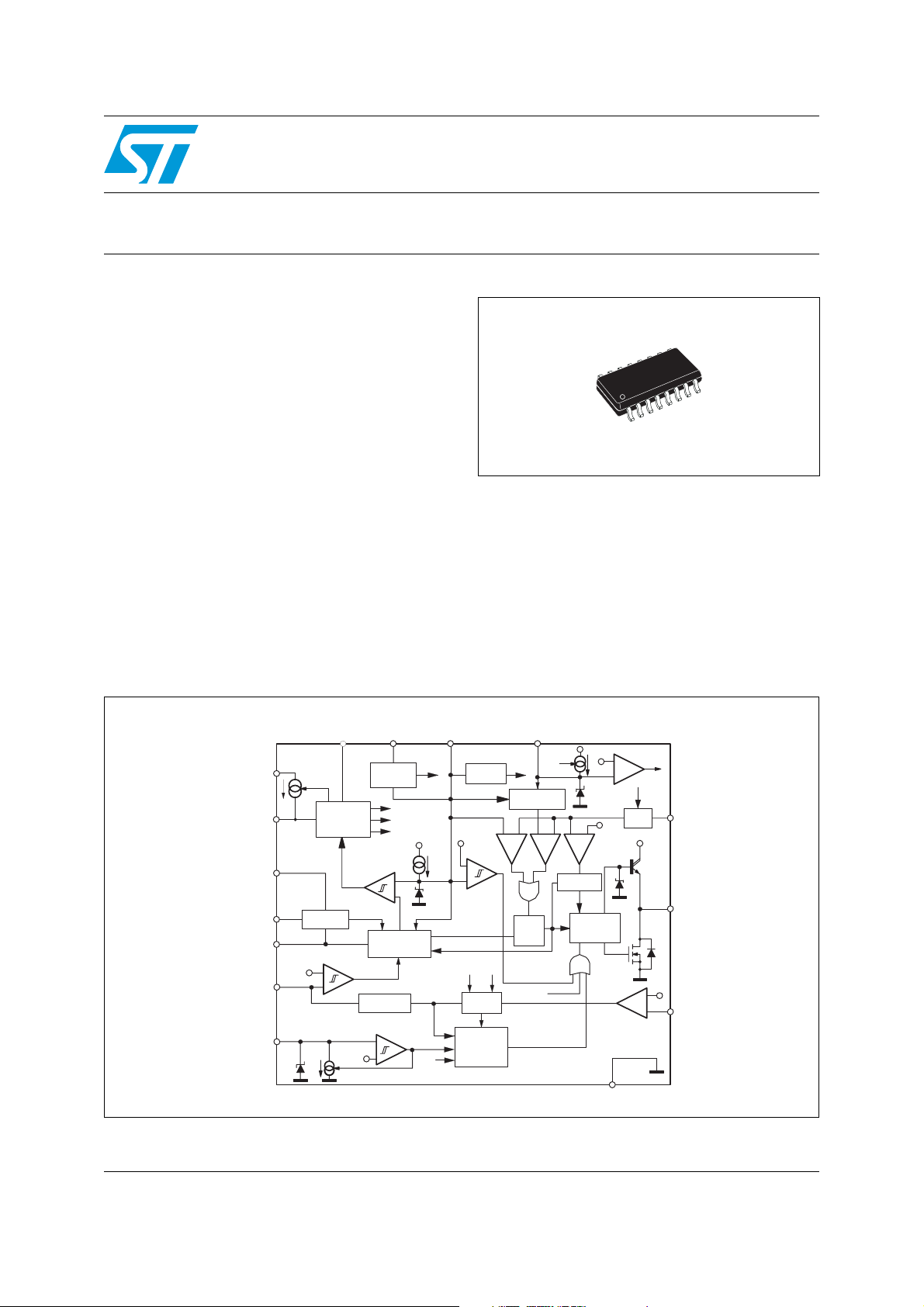
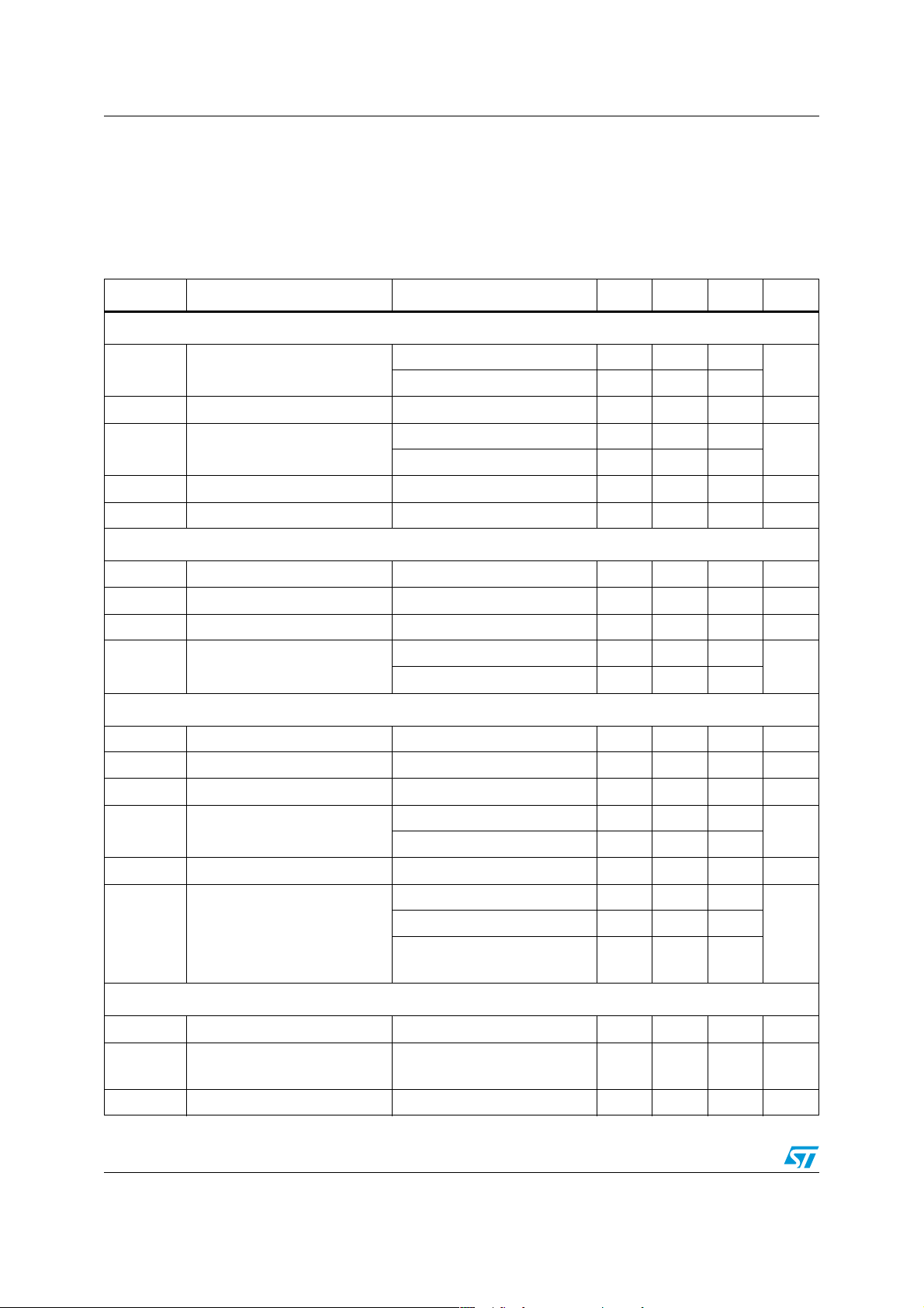
Figure 1. Block diagram
L6566BH
Multimode controller for SMPS
Datasheet — production data
SO16N
■ -600/+800 mA totem pole gate driver with
active pull-down during UVLO
■ SO16N package
Applications
■ Industrial SMPS
■ SMPS running off rectified 3-phase input line
COMP
915
TIME
OUT
LOW CLAMP
& DISABLE
Vth
V
CC
400 uA
+
-
5.7V
BURST-MODE
TIME
OVPL
OUT
OVP
LATCH
IC_LATCH
AC_ FAI L
UVLO
DISABLE
VFF
OFF2
LINE VOLTAGE
FEEDFORWARD
+-
OCPPWM
R
Q
S
OFF2
OVP
+-
V
CC
+-
Hiccup-mode
OCP logic
OCP2
DRIVER
7.7V
I
charge
6.4V
3
1.5 V
OVPL
+
Q
V
CC
14V
LEB
CS
7
4
GD
4.5V
-
+
DIS
8
FMOD
OSC
MOD E/S C
ZCD
AC_O K
VRE F
10
1
HV
I
HV
V
CC
5
6
13
12
100 mV
11
16
50 mV
3 V
VOLTAG E
REGULATOR
ADAP TIVE UVL O
OSCILL ATOR
-
+
15 µA
&
UVLO_ SHF
ZERO CURRENT
DETECTOR
OVERVOLTAGE
0.450V
0.485V
SS
14
SOFT-START
&
FAULT MNGT
Ref er e nc e
voltages
Internal supply
UVL O
-
+
MODE SELECTION
&
TURN -ON LO GIC
PROTECTION
-
+
April 2012 Doc ID 16610 Rev 2 1/51
This is information on a product in full production.
www.st.com
51

Contents L6566BH
Contents
1 Description . . . . . . . . . . . . . . . . . . . . . . . . . . . . . . . . . . . . . . . . . . . . . . . . . 6
2 Pin settings . . . . . . . . . . . . . . . . . . . . . . . . . . . . . . . . . . . . . . . . . . . . . . . . 8
2.1 Connections . . . . . . . . . . . . . . . . . . . . . . . . . . . . . . . . . . . . . . . . . . . . . . . . 8
2.2 Pin description . . . . . . . . . . . . . . . . . . . . . . . . . . . . . . . . . . . . . . . . . . . . . . 8
3 Electrical data . . . . . . . . . . . . . . . . . . . . . . . . . . . . . . . . . . . . . . . . . . . . . 11
3.1 Maximum rating . . . . . . . . . . . . . . . . . . . . . . . . . . . . . . . . . . . . . . . . . . . . 11
3.2 Thermal data . . . . . . . . . . . . . . . . . . . . . . . . . . . . . . . . . . . . . . . . . . . . . . 11
4 Electrical characteristics . . . . . . . . . . . . . . . . . . . . . . . . . . . . . . . . . . . . 12
5 Application information . . . . . . . . . . . . . . . . . . . . . . . . . . . . . . . . . . . . . 16
5.1 High voltage startup generator . . . . . . . . . . . . . . . . . . . . . . . . . . . . . . . . . 17
5.2 Zero-current detection and triggering block; oscillator block . . . . . . . . . . 19
5.3 Burst-mode operation at no load or very light load . . . . . . . . . . . . . . . . . . 22
5.4 Adaptive UVLO . . . . . . . . . . . . . . . . . . . . . . . . . . . . . . . . . . . . . . . . . . . . . 23
5.5 PWM control block . . . . . . . . . . . . . . . . . . . . . . . . . . . . . . . . . . . . . . . . . . 24
5.6 PWM comparator, PWM latch and voltage feedforward blocks . . . . . . . . 25
5.7 Hiccup-mode OCP . . . . . . . . . . . . . . . . . . . . . . . . . . . . . . . . . . . . . . . . . . 28
5.8 Frequency modulation . . . . . . . . . . . . . . . . . . . . . . . . . . . . . . . . . . . . . . . 29
5.9 Latched disable function . . . . . . . . . . . . . . . . . . . . . . . . . . . . . . . . . . . . . . 31
5.10 Soft-start and delayed latched shutdown upon overcurrent . . . . . . . . . . . 32
5.11 OVP block . . . . . . . . . . . . . . . . . . . . . . . . . . . . . . . . . . . . . . . . . . . . . . . . . 33
5.12 Brownout protection . . . . . . . . . . . . . . . . . . . . . . . . . . . . . . . . . . . . . . . . . 36
5.13 Slope compensation . . . . . . . . . . . . . . . . . . . . . . . . . . . . . . . . . . . . . . . . . 39
5.14 Summary of L6566BH power management functions . . . . . . . . . . . . . . . 39
6 Application examples and ideas . . . . . . . . . . . . . . . . . . . . . . . . . . . . . . 43
2/51 Doc ID 16610 Rev 2

L6566BH Contents
7 Package mechanical data . . . . . . . . . . . . . . . . . . . . . . . . . . . . . . . . . . . . 46
8 Order codes . . . . . . . . . . . . . . . . . . . . . . . . . . . . . . . . . . . . . . . . . . . . . . . 49
9 Revision history . . . . . . . . . . . . . . . . . . . . . . . . . . . . . . . . . . . . . . . . . . . 50
Doc ID 16610 Rev 2 3/51

List of tables L6566BH
List of tables
Table 1. Pin functions . . . . . . . . . . . . . . . . . . . . . . . . . . . . . . . . . . . . . . . . . . . . . . . . . . . . . . . . . . . . . 8
Table 2. Absolute maximum ratings . . . . . . . . . . . . . . . . . . . . . . . . . . . . . . . . . . . . . . . . . . . . . . . . . 11
Table 3. Thermal data. . . . . . . . . . . . . . . . . . . . . . . . . . . . . . . . . . . . . . . . . . . . . . . . . . . . . . . . . . . . 11
Table 4. Electrical characteristics . . . . . . . . . . . . . . . . . . . . . . . . . . . . . . . . . . . . . . . . . . . . . . . . . . . 12
Table 5. L6566BH light load management features . . . . . . . . . . . . . . . . . . . . . . . . . . . . . . . . . . . . . 40
Table 6. L6566BH protection . . . . . . . . . . . . . . . . . . . . . . . . . . . . . . . . . . . . . . . . . . . . . . . . . . . . . . 40
Table 7. External circuits that determine IC behavior upon OVP and OCP . . . . . . . . . . . . . . . . . . . 44
Table 8. SO16N mechanical data . . . . . . . . . . . . . . . . . . . . . . . . . . . . . . . . . . . . . . . . . . . . . . . . . . . 46
Table 9. Order codes . . . . . . . . . . . . . . . . . . . . . . . . . . . . . . . . . . . . . . . . . . . . . . . . . . . . . . . . . . . . 49
Table 10. Document revision history . . . . . . . . . . . . . . . . . . . . . . . . . . . . . . . . . . . . . . . . . . . . . . . . . 50
4/51 Doc ID 16610 Rev 2

L6566BH List of figures
List of figures
Figure 1. Block diagram . . . . . . . . . . . . . . . . . . . . . . . . . . . . . . . . . . . . . . . . . . . . . . . . . . . . . . . . . . . . 1
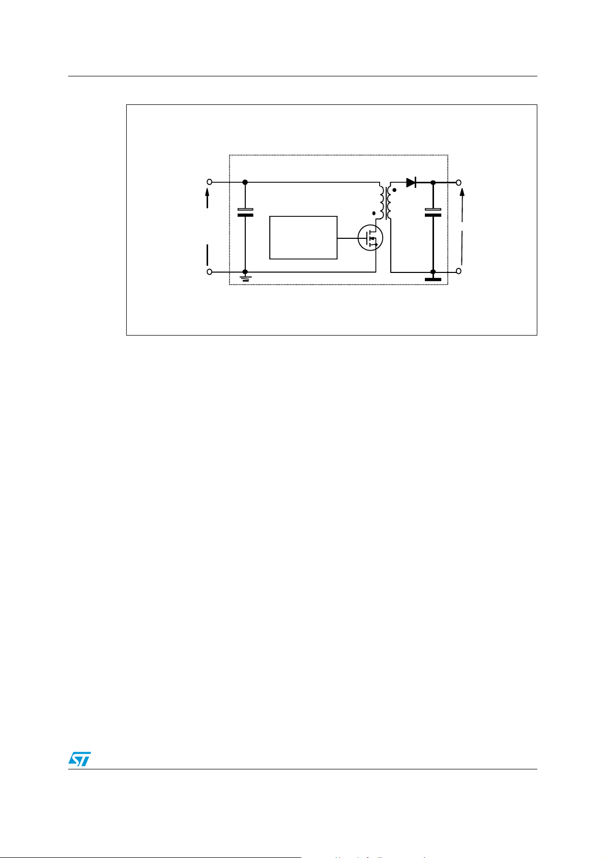
Figure 2. Typical system block diagram. . . . . . . . . . . . . . . . . . . . . . . . . . . . . . . . . . . . . . . . . . . . . . . . 7
Figure 3. Pin connection (through top view) . . . . . . . . . . . . . . . . . . . . . . . . . . . . . . . . . . . . . . . . . . . . 8
Figure 4. Multimode operation with QR option active . . . . . . . . . . . . . . . . . . . . . . . . . . . . . . . . . . . . 16
Figure 5. High voltage startup generator: internal schematic . . . . . . . . . . . . . . . . . . . . . . . . . . . . . . 17
Figure 6. Timing diagram: normal power-up and power-down sequences . . . . . . . . . . . . . . . . . . . . 18
Figure 7. Timing diagram showing short-circuit behavior (SS pin clamped at 5 V) . . . . . . . . . . . . . . 19
Figure 8. V
Figure 9. Drain ringing cycle skipping as the load is gradually reduced . . . . . . . . . . . . . . . . . . . . . . 20
Figure 10. Operation of ZCD, triggering and oscillator blocks (QR option active) . . . . . . . . . . . . . . . . 22
Figure 11. Load-dependent operating modes: timing diagrams . . . . . . . . . . . . . . . . . . . . . . . . . . . . . 23
Figure 12. Addition of an offset to the current sense lowers the burst-mode operation threshold . . . . 23
Figure 13. Adaptive UVLO block . . . . . . . . . . . . . . . . . . . . . . . . . . . . . . . . . . . . . . . . . . . . . . . . . . . . . 24
Figure 14. Possible feedback configurations that can be used with the L6566BH . . . . . . . . . . . . . . . 24
Figure 15. Externally controlled burst-mode operation by driving the COMP pin: timing diagram. . . . 25
Figure 16. Typical power capability change vs. input voltage in QR flyback converters . . . . . . . . . . . 26
Figure 17. Left: overcurrent setpoint vs. VFF voltage; right: line feedforward function block. . . . . . . . 27
Figure 18. Hiccup-mode OCP: timing diagram . . . . . . . . . . . . . . . . . . . . . . . . . . . . . . . . . . . . . . . . . . 29
Figure 19. Frequency modulation circuit . . . . . . . . . . . . . . . . . . . . . . . . . . . . . . . . . . . . . . . . . . . . . . . 30
Figure 20. Operation after latched disable activation: timing diagram . . . . . . . . . . . . . . . . . . . . . . . . . 32
Figure 21. Soft-start pin operation under different operating conditions and settings . . . . . . . . . . . . . 33
Figure 22. OVP function: internal block diagram . . . . . . . . . . . . . . . . . . . . . . . . . . . . . . . . . . . . . . . . . 34
Figure 23. OVP function: timing diagram . . . . . . . . . . . . . . . . . . . . . . . . . . . . . . . . . . . . . . . . . . . . . . . 35
Figure 24. Maximum allowed duty cycle vs. switching frequency for correct OVP detection. . . . . . . . 36
Figure 25. Brownout protection: internal block diagram and timing diagram . . . . . . . . . . . . . . . . . . . . 37
Figure 26. Voltage sensing techniques to implement brownout protection with the L6566BH . . . . . . 38
Figure 27. Slope compensation waveforms. . . . . . . . . . . . . . . . . . . . . . . . . . . . . . . . . . . . . . . . . . . . . 39
Figure 28. Typical low-cost application schematic . . . . . . . . . . . . . . . . . . . . . . . . . . . . . . . . . . . . . . . . 43
Figure 29. Typical full-feature application schematic (QR operation) . . . . . . . . . . . . . . . . . . . . . . . . . 43
Figure 30. Typical full-feature application schematic (FF operation) . . . . . . . . . . . . . . . . . . . . . . . . . . 44
Figure 31. Frequency foldback at light load (FF operation) . . . . . . . . . . . . . . . . . . . . . . . . . . . . . . . . 45
Figure 32. Latched shutdown upon mains overvoltage . . . . . . . . . . . . . . . . . . . . . . . . . . . . . . . . . . . . 45
Figure 33. SO16N package drawing . . . . . . . . . . . . . . . . . . . . . . . . . . . . . . . . . . . . . . . . . . . . . . . . . . 47
Figure 34. Recommended footprint (dimensions are in mm) . . . . . . . . . . . . . . . . . . . . . . . . . . . . . . . . 48
rating vs. temperature . . . . . . . . . . . . . . . . . . . . . . . . . . . . . . . . . . . . . . . . . . . . . . . . . 19
HV
Doc ID 16610 Rev 2 5/51

Description L6566BH
1 Description
The L6566BH is an extremely versatile current-mode primary controller IC, specifically
designed for high-performance offline flyback converters running off rectified 3-phase input
lines. It is also suited to single-stage, single-switch, input-current-shaping converters
(single-stage PFC) for applications that must comply with EN61000-3-2 or JEITA-MITI
regulations.
Both fixed-frequency (FF) and quasi-resonant (QR) operation are supported. The user can
choose either of the two depending on application needs. The device features an externally
programmable oscillator: it defines the converter switching frequency in FF mode and the
maximum allowed switching frequency in QR mode.
When FF operation is selected, the ICs work as a standard current-mode controller with a
maximum duty cycle limited to 70% min. The oscillator frequency can be modulated to
mitigate EMI emissions.
QR operation, when selected, occurs at heavy load and is achieved through a transformer
demagnetization sensing input that triggers MOSFET turn-on. Under some conditions, ZVS
(zero-voltage switching) can be achieved. The converter’s power capability rise with the
mains voltage is compensated by line voltage feedforward. At medium and light load, as the
QR operating frequency equals the oscillator frequency, a function (valley skipping) is
activated to prevent further frequency rise and keep the operation as close to ZVS as
possible.
With either FF or QR operation, at very light load the ICs enter a controlled burst-mode
operation that, along with the built-in, non-dissipative, high-voltage startup circuit and the
low quiescent current, helps keep the consumption from the mains low and meet energy
saving recommendations.
An innovative adaptive UVLO helps minimize the issues related to the fluctuations of the
self-supply voltage due to transformer parasites.
The protection functions included in this device are: not-latched input undervoltage
(brownout), output OVP (auto-restart or latch-mode selectable), a first-level OCP with
delayed shutdown to protect the system during overload or short-circuit conditions (autorestart or latch-mode selectable), and a second-level OCP that is invoked when the
transformer saturates or there is a short-circuit of the secondary diode. A latched disable
input allows easy implementation of OTP with an external NTC, while an internal shutdown
prevents IC overheating.
Programmable soft-start, leading-edge blanking on the current sense input for greater noise
immunity, slope compensation (in FF mode only), and a shutdown function for externally
controlled burst-mode operation or remote ON/OFF control complete the features of this
device.
6/51 Doc ID 16610 Rev 2
L6566BH Description
Figure 2. Typical system block diagram
FLYBAC K DC-DC CO NVERTER
Rectified
& Filtered
Mains
Voltage
L6566BH
V
outdc
Doc ID 16610 Rev 2 7/51
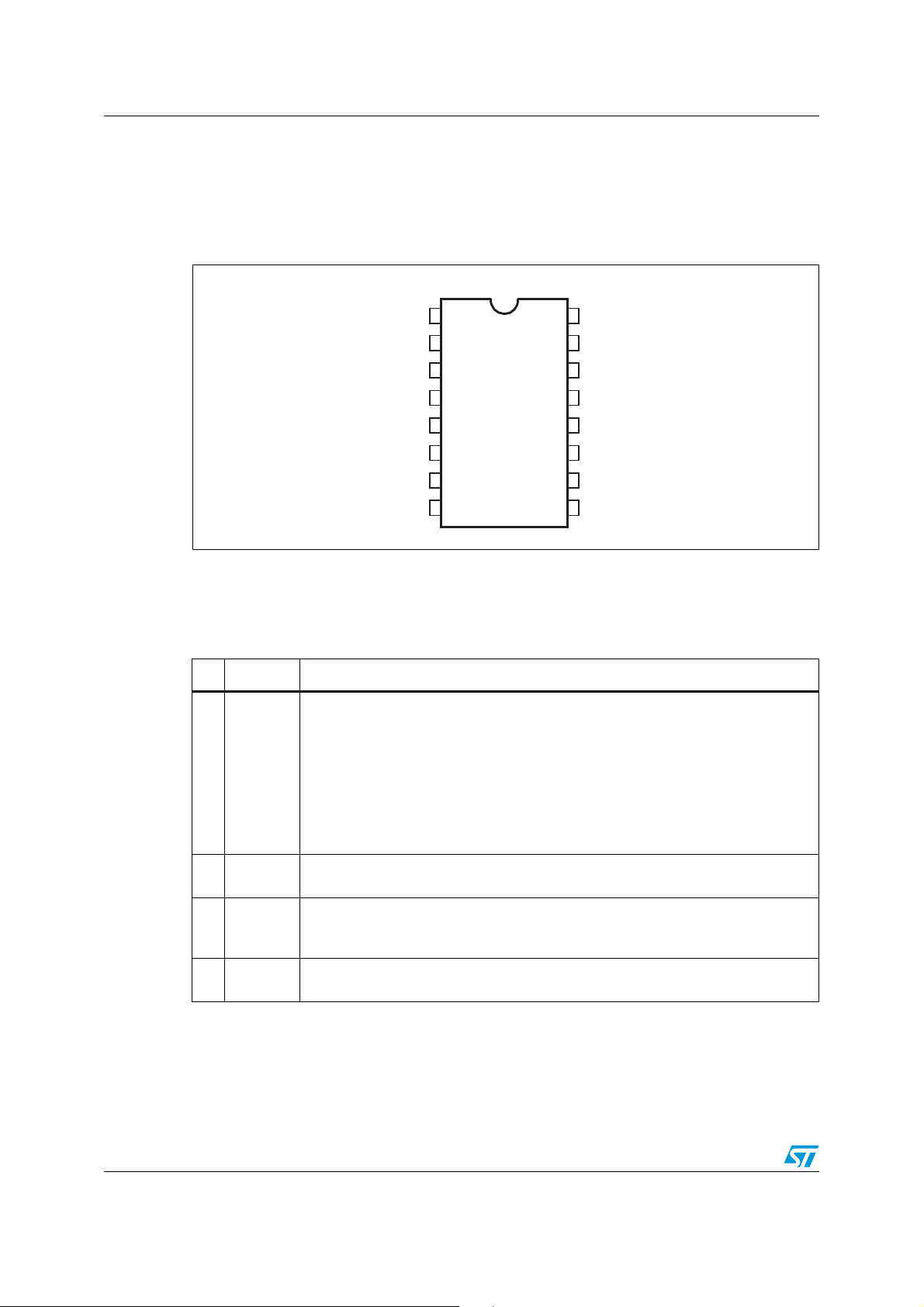
Pin settings L6566BH
2 Pin settings
2.1 Connections
Figure 3. Pin connection (through top view)
1
16
KO_CASVH
2.2 Pin description
Table 1. Pin functions
N° Pin Function
High voltage startup. The pin, able to withstand 840 V, is to be tied directly to the
rectified mains voltage. A 1 mA internal current source charges the capacitor
connected between the Vcc pin (5) and GND pin (3) until the voltage on the Vcc pin
reaches the turn-on threshold, it is then shut down. Normally, the generator is re-
1HVS
2N.C.
enabled when the Vcc voltage falls below 5 V to ensure a low power throughput
during short-circuit. Otherwise, when a latched protection is tripped the generator is
re-enabled 0.5 V below the turn-on threshold, to keep the latch supplied; or, when
the IC is turned off by the COMP pin (9) pulled low, the generator is active just
below the UVLO threshold to allow a faster restart.
Not internally connected. Provision for clearance on the PCB to meet safety
requirements.
N. C.
GND
GD
Vcc
FMOD
DIS
2
3
4
5
6
7
8
15
14
13
12
11
10
9
VFF
SS
OSC
MODE /S C
ZCD
FERVSC
COMP
AM11479v1
Ground. Current return for both the signal part of the IC and the gate drive. All of
3GND
4GD
8/51 Doc ID 16610 Rev 2
the ground connections of the bias components should be tied to a track going to
this pin and kept separate from any pulsed current return.
Gate driver output. The totem pole output stage is able to drive Power MOSFETs
and IGBTs with a peak current capability of 800 mA source/sink.

L6566BH Pin settings
Table 1. Pin functions (continued)
N° Pin Function
Supply voltage of both the signal part of the IC and the gate driver. The internal
high voltage generator charges an electrolytic capacitor connected between this
pin and GND (pin 3) as long as the voltage on the pin is below the turn-on threshold
5Vcc
6FMOD
7CS
of the IC, after that it is disabled and the chip is turned on. The IC is disabled as the
voltage on the pin falls below the UVLO threshold. This threshold is reduced at light
load to counteract the natural reduction of the self-supply voltage. Sometimes a
small bypass capacitor (0.1 µF typ.) to GND might be useful to obtain a clean bias
voltage for the signal part of the IC.
Frequency modulation input. When FF mode operation is selected, a capacitor
connected from this pin to GND (pin 3) is alternately charged and discharged by
internal current sources. As a result, the voltage on the pin is a symmetrical
triangular waveform with the frequency related to the capacitance value. By
connecting a resistor from this pin to pin 13 (OSC) it is possible to modulate the
current sourced by the OSC pin and then the oscillator frequency. This modulation
is to reduce the peak value of EMI emissions by means of a spread-spectrum
action. If the function is not used, the pin is left open.
Input to the PWM comparator. The current flowing in the MOSFET is sensed
through a resistor, the resulting voltage is applied to this pin and compared with an
internal reference to determine MOSFET turn-off. The pin is equipped with 150 ns
min. blanking time after the gate-drive output goes high for improved noise
immunity. A second comparison level located at 1.5 V latches the device OFF and
reduces its consumption in the case of transformer saturation or secondary diode
short-circuit. The information is latched until the voltage on the Vcc pin (5) goes
below the UVLO threshold, therefore resulting in intermittent operation. A logic
circuit improves sensitivity to temporary disturbances.
8DIS
9COMP
10 VREF
IC latched disable input. Internally, the pin connects a comparator that, when the
voltage on the pin exceeds 4.5 V, latches OFF the IC and brings its consumption to
a lower value. The latch is cleared as the voltage on the Vcc pin (5) goes below the
UVLO threshold, but the HV generator keeps the Vcc voltage high (see pin 1
description). It is then necessary to recycle the input power to restart the IC. For a
quick restart, pull pin 16 (AC_OK) below the disable threshold (see pin 16
description). Bypass the pin with a capacitor to GND (pin 3) to reduce noise pickup. Ground the pin if the function is not used.
Control input for loop regulation. The pin is driven by the phototransistor (emittergrounded) of an optocoupler to modulate its voltage by modulating the current
sunk. A capacitor placed between the pin and GND (3), as close to the IC as
possible to reduce noise pick-up, sets a pole in the output-to-control transfer
function. The dynamics of the pin are in the 2.5 to 5 V range. A voltage below an
internally defined threshold activates burst-mode operation. The voltage at the pin
is bottom-clamped at about 2 V. If the clamp is externally overridden and the
voltage is pulled below 1.4 V, the IC shuts down.
An internal generator furnishes an accurate voltage reference (5 V ± 2%) that can
be used to supply few mA to an external circuit. A small film capacitor (0.1 µF typ.),
connected between this pin and GND (3), is recommended to ensure the stability of
the generator and to prevent noise from affecting the reference. This reference is
internally monitored by a separate auxiliary reference and any failure or drift causes
the IC to latch OFF.
Doc ID 16610 Rev 2 9/51

Pin settings L6566BH
Table 1. Pin functions (continued)
N° Pin Function
Transformer demagnetization sensing input for quasi-resonant operation and OVP
input. The pin is externally connected to the transformer’s auxiliary winding through
a resistor divider. A negative-going edge triggers MOSFET turn-on if QR mode is
11 ZCD
12 MODE/SC
13 OSC
14 SS
15 VFF
selected.
A voltage exceeding 5 V shuts the IC down and brings its consumption to a lower
value (OVP). Latch OFF or auto-restart mode is selectable externally. This function
is strobed and digitally filtered to increase noise immunity.
Operating mode selection. If the pin is connected to the VREF pin (7), quasiresonant operation is selected, the oscillator (pin 13, OSC) determines the
maximum allowed operating frequency.
Fixed-frequency operation is selected if the pin is not tied to VREF, in which case
the oscillator determines the actual operating frequency, the maximum allowed
duty cycle is set at 70% min. and the pin delivers a voltage ramp synchronized to
the oscillator when the gate-drive output is high; the voltage delivered is zero while
the gate-drive output is low. The pin is to be connected to pin CS (7) via a resistor
for slope compensation.
Oscillator pin. The pin is an accurate 1 V voltage source, and a resistor connected
from the pin to GND (pin 3) defines a current. This current is internally used to set
the oscillator frequency that defines the maximum allowed switching frequency of
the L6566BH, if working in QR mode, or the operating switching frequency if
working in FF mode.
Soft-start current source. At startup, a capacitor Css between this pin and GND
(pin 3) is charged with an internal current generator. During the ramp, the internal
reference clamp on the current sense pin (7, CS) rises linearly starting from zero to
its final value, therefore causing the duty cycle to increase progressively starting
from zero as well. During soft-start the adaptive UVLO function and all functions
monitoring the COMP pin are disabled. The soft-start capacitor is discharged
whenever the supply voltage of the IC falls below the UVLO threshold. The same
capacitor is used to delay IC shutdown (latch OFF or auto-restart mode selectable)
after detecting an overload condition (OLP).
Line voltage feedforward input. The information on the converter’s input voltage is
fed into the pin through a resistor divider and is used to change the setpoint of the
pulse-by-pulse current limitation (the higher the voltage, the lower the setpoint).
The linear dynamics of the pin ranges from 0 to 3 V. A voltage higher than 3 V
makes the IC stop switching. If feedforward is not desired, tie the pin to GND (pin 3)
directly if a latch-mode OVP is not required (see pin 11, ZCD) or through a 10 kΩ
min. resistor if a latch-mode OVP is required. Bypass the pin with a capacitor to
GND (pin 3) to reduce noise pick-up.
Brownout protection input. A voltage below 0.45 V shuts down (not latched) the IC,
lowers its consumption and clears the latch set by latched protection (DIS > 4.5 V,
SS > 6.4 V, VFF > 6.4 V). IC operation is re-enabled as the voltage exceeds 0.45 V.
16 AC_OK
10/51 Doc ID 16610 Rev 2
The comparator is provided with current hysteresis: an internal 15 µA current
generator is ON as long as the voltage on the pin is below 0.45 V and is OFF if this
value is exceeded. Bypass the pin with a capacitor to GND (pin 3) to reduce noise
pick-up. Tie to Vcc with a 220 to 680 kW resistor if the function is not used.
L6566BH Electrical data
3 Electrical data
3.1 Maximum rating
Table 2. Absolute maximum ratings
Symbol Pin Parameter Value Unit
V
HVS
I
HVS
V
CC
V
FMOD
V
max
V
max
I
ZCD
V
MODE/SC
V
OSC
P
TOT
T
STG
T
J
1 Voltage range (referred to ground) @ 25 °C -0.3 to 840 V
1 Output current Self-limited
5 IC supply voltage (Icc = 20 mA) Self-limited
6 Voltage range -0.3 to 2 V
7, 8, 10, 14 Analog inputs and outputs -0.3 to 7 V
9, 15, 16 Maximum pin voltage (Ipin ≤ 1 mA) Self-limited
11 Zero-current detector max. current ±5 mA
12 Voltage range -0.3 to 5.3 V
13 Voltage range -0.3 to 3.3 V
3.2 Thermal data
Table 3. Thermal data
Symbol Parameter Value Unit
Power dissipation @ TA = 50 °C 0.75 W
Storage temperature -55 to 150 °C
Junction operating temperature range -40 to 150 °C
R
thJA
Thermal resistance junction to ambient 120 °C/W
Doc ID 16610 Rev 2 11/51
Electrical characteristics L6566BH
4 Electrical characteristics
(TJ = -25 to 125 °C, VCC = 12, CO = 1 nF; MODE/SC = V
, RT = 20 kΩ from OSC to GND,
REF
unless otherwise specified.)
Table 4. Electrical characteristics
Symbol Parameter Test condition Min. Typ. Max. Unit
Supply voltage
Vcc Operating range after turn-on
Vcc
Vcc
Hys Hysteresis V
V
Supply current
I
start-up
I
q
Icc Operating supply current MODE/SC open 4 4.6 mA
I
qdis
V
> V
COMP
V
COMP
Turn-on threshold
On
Turn-off threshold
Off
Zener voltage Icc = 20 mA, IC disabled 23 25 27 V
Z
(1)
(1)
(1)
COMP
V
V
= V
COMP
COMP
> V
COMPL
COMPO
> V
= V
COMPL
COMPL
COMPO
10.6 23
823
13 14 15 V
9.4 10 10.6
7.2 7.6 8.0
4V
Startup current Before turn-on, Vcc = 13 V 200 250 µA
Quiescent current After turn-on, V
IC disabled
(2)
ZCD
= V
= 1 V 2.6 2.8 mA
CS
330 2500
Quiescent current
IC latched OFF 440 500
V
V
µA
High voltage startup generator
V
HV
V
HVstart
I
charge
I
HV, ON
I
HV, OFF
V
CCrestart
Breakdown voltage
Start voltage I
Vcc charge current VHV > V
ON-state current
OFF-state leakage current VHV = 400 V 40 µA
Vcc restart voltage
Reference voltage
V
V
I
REF
REF
REF
Output voltage
To t a l va r ia ti on
Short-circuit current V
(3)
I
< 100 µA @ 25 °C 840 V
HV
< 100 µA 65 80 100 V
Vcc
, Vcc > 3 V 0.55 0.85 1 mA
Hvstart
V
> V
HV
> V
V
HV
, Vcc > 3 V 1.6
Hvstart
, Vcc = 0 0.8
Hvstart
Vcc falling 4.4 5 5.6
(1)
IC latched OFF 12.5 13.5 14.5
(1)
Disabled by
V
< V
COMP
(1)
TJ = 25 °C; I
I
REF
COMPOFF
REF
= 1 to 5 mA,
= 1 mA 4.95 5 5.05 V
Vcc = 10.6 to 23 V
= 0 10 30 mA
REF
9.4 10 10.6
4.9 5.1 V
mA
V
12/51 Doc ID 16610 Rev 2
L6566BH Electrical characteristics
Table 4. Electrical characteristics (continued)
Symbol Parameter Test condition Min. Typ. Max. Unit
Sink capability in UVLO Vcc = 6 V; Isink = 0.5 mA 0.2 0.5 V
V
OV
Overvoltage threshold 5.3 5.7 V
Internal oscillator
Oscillation frequency
Voltage reference
Maximum duty cycle
V
D
f
sw
OSC
max
Brownout protection
Vth Threshold voltage
I
Hys
V
AC_OK_CL
Current hysteresis Vcc > 5 V, V
Clamp level
Line voltage feedforward
I
VFF
V
VFF
V
OFF
V
VFFlatch
Input bias current
Linear operation range 0 to 3 V
IC disable voltage 3 3.15 3.3 V
Latch OFF/clamp level V
Kc Control voltage gain
K
FF
Feedforward gain
Current sense comparator
(3)
(4)
Operating range 10 300
T
= 25 °C, V
J
MODE/SC = open
Vcc =12 to 23 V, V
MODE/SC = open
(4)
MODE/SC = open,
V
= 5 V
COMP
ZCD
= 0,
ZCD
= 0,
95 100 105
kHz
93 100 107
0.9711.03V
70 75 %
Voltage falling (turn-off) 0.432 0.450 0.468 V
Voltage rising (turn-on) 0.452 0.485 0.518 V
= 0.3 V 121518µA
VFF
(1)
V
V
V
V
I
VFF
ZCD
ZCD
VFF
VFF
= 100 µA 3 3.15 3.3 V
AC_OK
= 0 to 3 V, V
> V
ZCDth
> V
ZCDth
= 1 V, V
= 1 V, V
COMP
COMP
< V
ZCD
ZCDth
-0.7 -1 mA
6.4 V
= 4 V 0.4 V/V
= 4 V 0.04 V/V
-1 µA
I
CS
t
LEB
td
(H-L)
V
CSx
V
CSdis
PWM control
V
COMPHI
Input bias current VCS = 0 -1 µA
Leading edge blanking 150 250 300 ns
Delay to output 100 ns
V
Overcurrent setpoint
Hiccup-mode OCP level
Upper clamp voltage I
= V
COMP
= V
COMP
V
= V
COMP
(1)
= 0 5.7 V
COMP
COMPHI
COMPHI
COMPHI
, V
= 0 V 0.92 1 1.08
VFF
, V
= 1.5 V 0.45 0.5 0.55
VFF
, V
= 3.0 V 0 0.1
VFF
1.4 1.5 1.6 V
VV
Doc ID 16610 Rev 2 13/51
Electrical characteristics L6566BH
Table 4. Electrical characteristics (continued)
Symbol Parameter Test condition Min. Typ. Max. Unit
V
COMPLO
V
COMPSH
I
COMP
R
COMP
V
COMPBM
Lower clamp voltage I
Linear dynamics upper limit
Max. source current V
Dynamic resistance V
Burst-mode threshold
SOURCE
(1)
(1)
(1)
= -1 mA 2.0 V
V
= 0 V 4.855.2V
VFF
= 3.3 V 320 400 480 µA
COMP
= 2.6 to 4.8 V 25 kΩ
COMP
2.52 2.65 2.78
MODE/SC = open 2.7 2.85 3
Hys Burst-mode hysteresis 20 mV
I
CLAMPL
V
COMPOFF
V
COMPO
V
COMPL
Lower clamp capability V
= 2 V -3.5 -1.5 mA
COMP
Disable threshold Voltage falling 1.4 V
(4)
Level for lower UVLO OFF
threshold (voltage falling)
Level for higher UVLO OFF
threshold (voltage rising)
2.61 2.75 2.89
(4)
MODE/SC = open 3.02 3.15 3.28
(4)
(4)
MODE/SC = open 3.41 3.55 3.69
2.93.053.2
Zero-current detector/overvoltage protection
V
ZCDH
V
ZCDL
V
ZCDA
V
ZCDT
I
ZCD
I
ZCDsrc
I
ZCDsnk
T
BLANK1
V
ZCDth
T
BLANK2
Upper clamp voltage I
Lower clamp voltage I
Arming voltage
Triggering voltage
Internal pull-up
Source current capability V
Sink current capability V
Turn-on inhibit time After gate-drive going low 2.5 µs
OVP threshold 4.85 5 5.15 V
OVP strobe delay After gate-drive going low 2 µs
= 3 mA 5.4 5.7 6 V
ZCD
= - 3 mA -0.4 V
ZCD
(1)
Positive-going edge 85 100 115 mV
(1)
Negative-going edge 30 50 70 mV
V
COMP
V
ZCD
ZCD
ZCD
< V
COMPSH
< 2 V, V
= V
ZCDL
= V
ZCDH
COMP
= V
COMPHI
-130 -100 -70
-3 mA
3mA
-1
Latched shutdown function
V
V
V
µA
I
V
OTP
OTP
Input bias current V
Disable threshold
DIS
(1)
= 0 to V
OTP
4.32 4.5 4.68 V
Thermal shutdown
Vth Shutdown threshold 160 °C
Hys Hysteresis 50 °C
External oscillator (frequency modulation)
f
FMOD
Oscillation frequency C
= 0.1 µF 600 750 900 Hz
MOD
--- Usable frequency range 0.05 15 kHz
14/51 Doc ID 16610 Rev 2
-1 µA
L6566BH Electrical characteristics
Table 4. Electrical characteristics (continued)
Symbol Parameter Test condition Min. Typ. Max. Unit
V
V
I
FMOD
pk
vy
Peak voltage
Valley voltage 0.5 V
Charge/discharge current 150 µA
Mode selection / slope compensation
(4)
1.5 V
MODE
th
SC
pk
SC
vy
Soft-start
I
SS1
I
SS2
I
SSdis
V
SSclamp
V
SSDIS
V
SSLAT
Gate driver
Threshold for QR operation 3 V
Ramp peak
(MODE/SC = open)
Ramp starting value
(MODE/SC = open)
Ramp voltage
(MODE/SC = open)
Source capability
(MODE/SC = open)
Charge current
R
pin HIGH, V
R
GD pin HIGH
GD pin LOW 0 V
V
TJ = 25 °C, VSS < 2 V,
V
TJ = 25 °C, VSS > 2 V,
V
= 3 kΩ to GND, GD
S-COMP
= 3 kΩ to GND,
S-COMP
S-COMP = VS-COMPpk
= 4 V
COMP
= V
COMP
COMP
COMPHi
= 5 V
1.7 V
0.3 V
0.8 mA
14 20 26
µA
3.556.5
Discharge current VSS > 2 V 3.556.5µA
High saturation voltage V
Disable level
Latch OFF level V
= 4 V 2 V
COMP
(1)
V
COMP
COMP
= V
= V
COMPHi
COMPHi
4.8555.15V
6.4 V
V
GDH
V
GDL
I
sourcepk
I
sinkpk
t
t
V
GDclamp
Output high voltage I
Output low voltage I
Output source peak current -0.6 A
Output sink peak current 0.8 A
Fall time 40 ns
f
Rise time 50 ns
r
Output clamp voltage I
UVLO saturation Vcc = 0 to V
1. Parameters tracking one another.
2. See
3. For the thermal behavior, refer to
4. The voltage feedforward block output is given by:
Table 6 on page 18
and
Table 7 on page 44
Figure 8
.
GDsource
GDsink
GDsource
.
= 5 mA, Vcc = 12 V 9.8 11 V
= 100 mA 0.75 V
= 5 mA; Vcc = 20 V 10 11.3 15 V
ccon, Isink = 1 mA 0.9 1.1 V
Doc ID 16610 Rev 2 15/51
Application information L6566BH
5 Application information
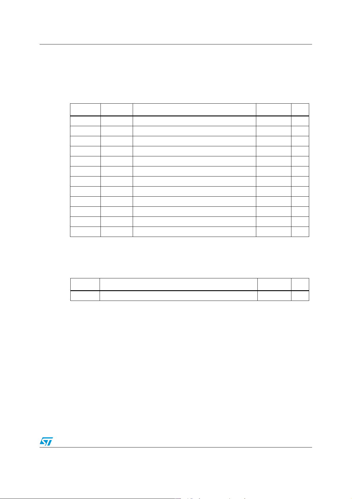
The L6566BH is a versatile peak-current-mode PWM controller specific to offline flyback
converters. The device allows either fixed-frequency (FF) or quasi-resonant (QR) operation,
selectable with the MODE/SC pin (12): forcing the voltage on the pin over 3 V (e.g. by tying
it to the 5 V reference externally available at the VREF pin, 10) activates QR operation,
otherwise the device is FF-operated.
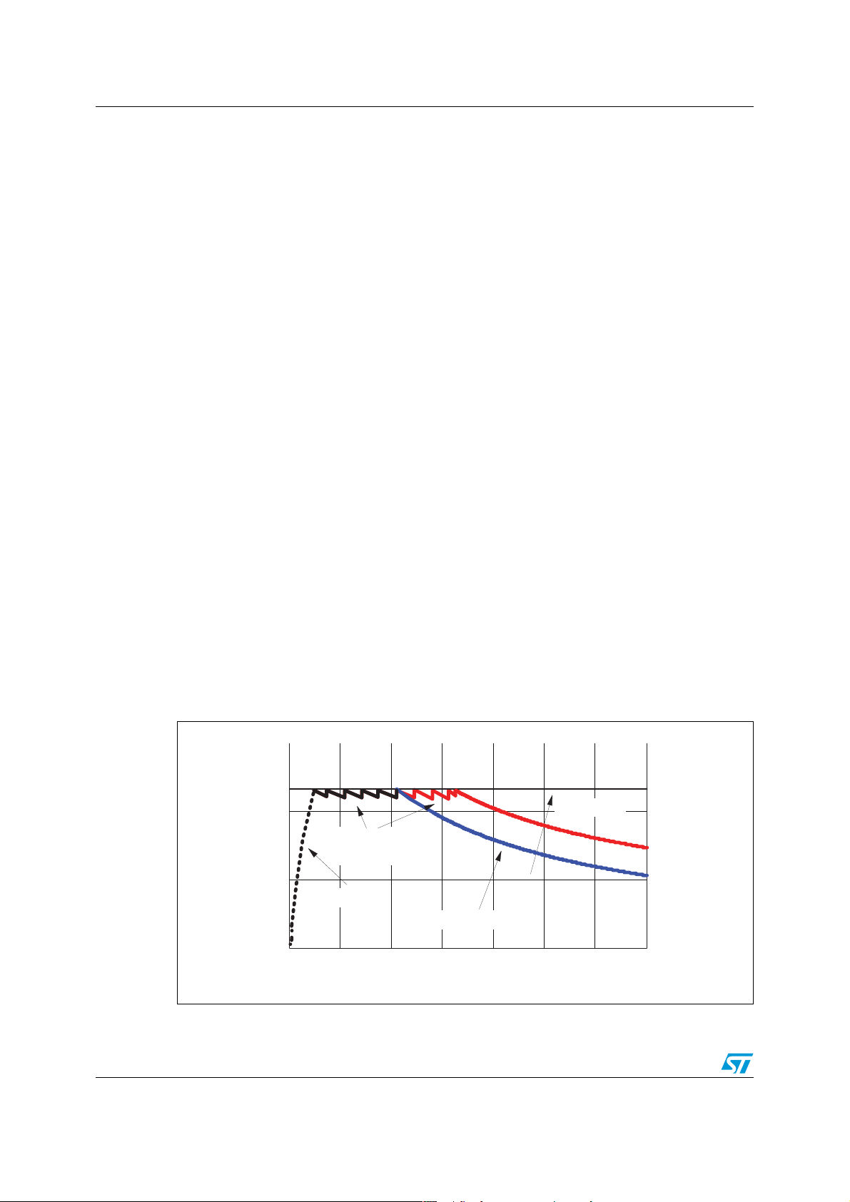
Irrespective of the operating option selected by pin 12, the device is able to work in different
modes, depending on the converter’s load conditions. If QR operation is selected (see
Figure 4
1. QR mode at heavy load. Quasi-resonant operation lies in synchronizing MOSFET turn-
2. Valley-skipping mode at medium/ light load. The externally programmable oscillator of
3. Burst-mode with no or very light load. When the load is extremely light or disconnected,
):
on to the transformer’s demagnetization by detecting the resulting negative-going edge
of the voltage across any winding of the transformer. Then, the system works close to
the boundary between discontinuous (DCM) and continuous conduction (CCM) of the
transformer. As a result, the switching frequency is different for different line/load
conditions (see the hyperbolic-like portion of the curves in
Figure 4
). Minimum turn-on
losses, low EMI emission and safe behavior in short-circuit are the main benefits of this
kind of operation.
the L6566BH, synchronized to MOSFET turn-on, enables the user to define the
maximum operating frequency of the converter. As the load is reduced, MOSFET turnon no longer occurs on the first valley but on the second one, the third one and so on.
In this way the switching frequency no longer increases (piecewise linear portion in
Figure 4
).
the converter enters a controlled on/off operation with constant peak current.
Decreasing the load then results in frequency reduction, which can go down even to
few hundred hertz, therefore minimizing all frequency-related losses and making it
easier to comply with energy saving regulations or recommendations. With the peak
current very low, no issue of audible noise arises.
Figure 4. Multimode operation with QR option active
f
osc
Valley-skipping
f
sw
0
0
16/51 Doc ID 16610 Rev 2
mode
Burst- m ode
Quasi-resonant mode
P
in
Input voltage
Pinmax
AM11480v1
 Loading...