

现货库存、技术资料、百科信息、热点资讯,精彩尽在鼎好!
QUASI-RESONANT SMPS CONTROLLER
■ QUASI-RESONANT (QR) ZERO-VOLTAGE-
SWITCHING (ZVS) TOPOLOGY
■ LINE FEED FORWARD TO DELIVER
CONSTANT POWER vs. MAINS CHANGE
■ FREQUENCY FOLDBACK FOR OP TI MU M
STANDBY EFFICI EN CY
■ PULSE-BY-PULSE & HICCUP-MODE OCP
■ ULTRA-LOW START-UP (< 70µA) AND
QUIESCENT CURRENT (< 3.5mA)
■ DISABLE FUNCTION (ON/OFF CONTROL)
■ 1% PRECISION (@ T
REFERENCE VOLTAGE
■ ±400mA TO TE M POLE GATE DR IV E R WI TH
UVLO PULL-DOWN
■ BLUE ANGEL, ENERGY STAR, ENERGY
2000 COMPLIANT
APPLICATIONS
■ TV/MONITOR SMPS
■ AC-DC ADAPTERS/CHARGERS
■ DIGITAL CONSUMER
■ PRINTERS, FAX MACHINES,
PHOTOCOPIERS AND SCANNERS
= 25°C) INTERNAL
j
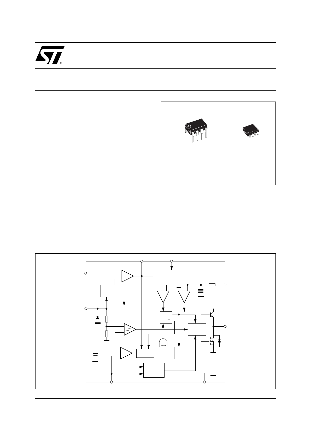
L6565
DIP8(Minidip) SO-8
ORDERING NUMB ERS :
L6565N L6565D
DESCRIPTION
The L6565 is a current-mode primary controller IC,
specifically designed to build offline Quasi-resonant
ZVS (Zero Voltage Switching at switch turn-on) flyback converters.
Quasi-resonant operation is achieved by means of a
transformer demagnetization sensing input that triggers MOSFET's turn-on.
BLOCK DIAGRAM
January 2003
INV
V
COMP
23
1
2.5V
REGULATOR
CC
20V
R2
2.1V
1.6V
5
VOLTAGE
R1
REF2
V
ZERO CURRENT
Hiccup-mode
ZCD
-
+
INTERNAL
SUPPLY
+
-
DETECTOR
+
-
OCP
UVLO
Blanki ng
BLANKING
DISABLE
START
VFF
LINE VOLTAGE
FEEDFORWARD
2 V
+-
RSQ
Q
STARTER
Starter
STOP
+-
Hiccup-mode
OCP
DRIVER
6
GND
40K
5pF
VCC8
4
CS
7
GD
1/17
L6565
DESCRIPTION
(continued)
Converter's power capability variations with the mains voltage are compensated by line voltage feedforward.
At light load the device features a special function that automatically lowers the operating frequency still maintaining the operation as close to ZVS as possible. In addition to very low start-up and quiescent currents, this
feature helps keep low the consumption from the mains at light load and be Blue Angel and Energy Star compliant.
The IC includes also a disable function, an on-chip filter on current sense, an error amplifier with a precise reference voltage for primary regulation and an effective two-level overcurrent protection.
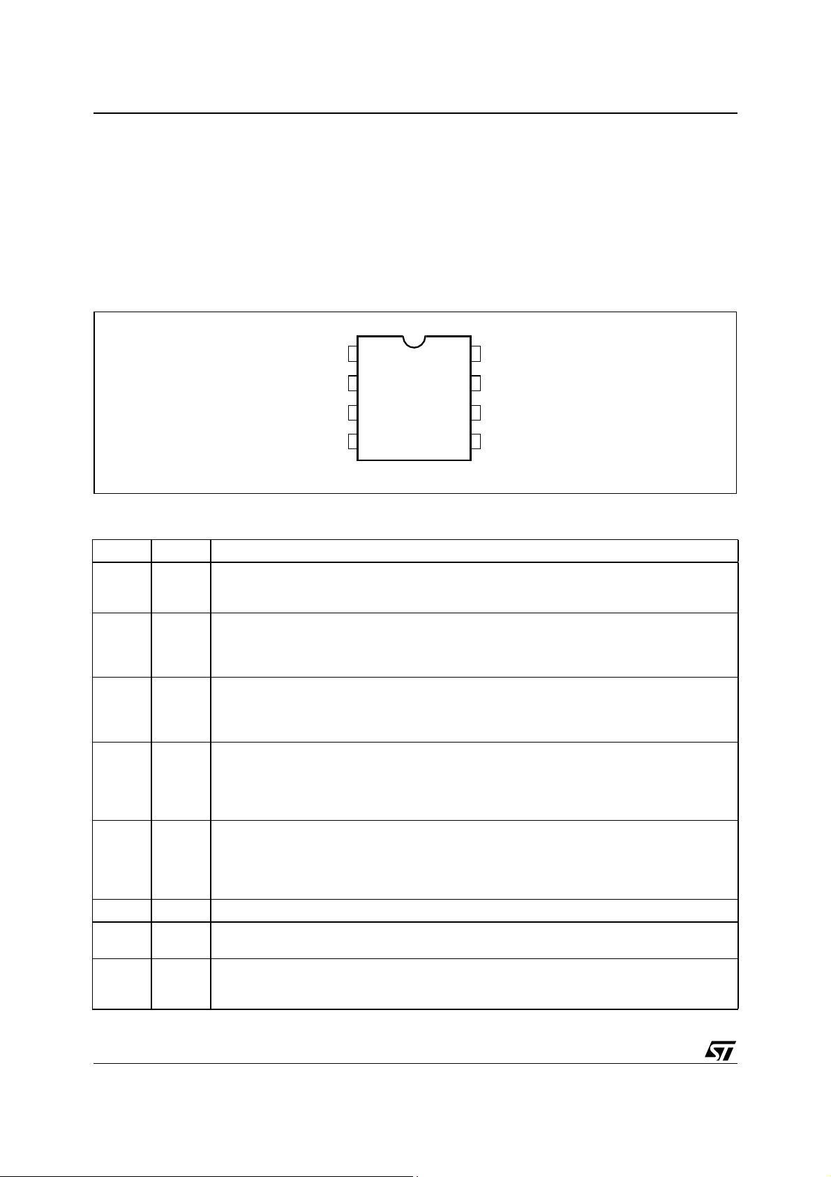
PIN CONNECTION
(Top view, Minidip and SO8)
INV
COMP
VFF
CS
1
2
3
4
Vcc
8
7
GD
GND
6
ZCD
5
PIN DESCRIPTION
N° Name Function
1 INV Inverting input of the error amplifier. The informatio n on the output voltage is fed into the pin
2 COMP Output of the error amplifie r. Typically, a compensat ion network is placed between this pin and
3 VFF Line voltage feedforward. The information on the converter’s input voltage is fed into the pin
4 CS Input to the P WM comparator. The primar y current is sense d through a resistor, the result ing
5 ZCD Transformer’s demagnetization sensing input for Quasi-Resonant operation. Alternately,
6 GND Ground. Current return for both the signal part of the IC and the gate driver.
7 GD Gate d river output. Th e totem pole output stag e is able to d rive power MOSFET ’s and IGBT’s
8 Vcc Supply Voltage of both the signal part of the IC and the gate driver. An electrolytic capacitor is
through either a res istor divider (primary reg ulation) or an optocoupler (second ary feedback).
This pin can be grounded in some secondary feedback schemes (see pin 2).
the INV pin to a chieve stability and good dy namic per forman ce o f the voltage con trol lo op. With
secondar y feedback, the pin can be also driven directly by an optocoupler to control PWM by
modulating the current sunk from the pin (with the INV pin grounded).
through a resistor divider and is used to change the setpoint of the pulse-by-pulse current
limitation (the higher the voltage, the lower the setpoint). If this function is not desired the pin will
be grounded and the current limitation setpoint will be maximum.
voltage is applied to this pin and co mpared with an inter nal reference to determ ine MOSFET’s
turn-off. The inter nal reference is clamped at a value, which defines the pulse-by-pulse current
limitation setpo int, d epen ding on th e voltage at p in VF F. If the sig nal a t the pin C S exceeds 2 V,
the gate driver will be disabled (Hiccup-mode OCP).
synchronizatio n input for an external signal. A nega tive-going edge triggers MO SFET’s turn- on.
The trigger cir cuit is blanked for a minimum of 3 .5 µs after MO SFET tur n-off, for safe operation
under short circuit conditions and frequency foldback. If the pin is grounded the IC will be
disabled.
with a peak current of 400 mA (source and sink).
connected b etween this pin an d ground. A resist or connected from this pin to the converter’s
input bulk capacitor will be typically used to start up the device.
2/17
THERMAL DATA
Symbol Parameter SO8 Minidip Unit
L6565
R
th j-amb
Max. Thermal Resistance, Junction-to-ambient 150 100 °C/W
ABSOLUTE MAXIMUM RATINGS
Symbol Pin Parameter Value Unit
I
Vcc
I
GD
INV, COMP,
8ICC + I
Z
7 Output Totem Pole Peak Current (2 µs) ±700 mA
1, 2, 3 4 Analog Inputs & Outputs -0.3 to 7 V
30 mA
VFF, CS
I
ZCD
5 Zero Current Detector 50 (source)
-10 (sink)
P
tot
T
j
T
stg
Power Dissipation @T
= 50°C (Minidip)
amb
(SO8)
1
0.65
Junction Temperature Operating range -40 to 150 °C
Storage Temperature -55 to 150 °C
ELECTRICAL CHARACTERISTCS
(Tj = -25 to 125°C, VCC = 12V, Co = 1nF; unless otherwise specified)
Symbol Parameter Test Condition Min. Typ. Max. Unit
SUPPLY VOLTAGE
V
V
CCOn
V
CCOff
Hys Hysteresis 3.65 4 4.3 V
V
SUPPLY CURRENT
I
start-up
I
LINE FEEDFORWARD
I
VFF
V
VFF
ERROR AMPLIFIER
V
I
INV
Operating range After turn-on 10.3 18
cc
Turn-on threshold 12.5 13.5 14 .5 V
Turn-off threshold 8.7 9.5 10.3 V
Zener Voltage Icc = 25 mA 18 20 22 V
Z
Start-up Current
I
Quiescent Current After turn-on 2.3 3.5 mA
q
Operating Supply Current @ 70 kHz 3.5 5 mA
CC
Quiescent Current During Hiccup-mode OCP 1.6 3.5 mA
I
q
Quiescent Current V
I
q
Input Bias Current V
Before turn-on, V
< V
ZCD
VFF
, VCC>V
DIS
= 0 to 3 V -1 µA
CC
= 12V
CCOff
45 70 µA
1.4 2.1 mA
Operating Range 0 to 3 V
K Gain
Voltage Feedback Input
INV
Threshold
V
= 1.5V, V
VFF
T
= 25°C 2.465 2.5 2.535 V
amb
COMP
= 4V
12V < VCC < 18V 2.44 2.56
0.16
Line Regulation Vcc = 12 to 18V 2 5 mV
Input Bias Current -0.1 - 1 µA
mA
W
3/17
L6565
ELECTRICAL CHARACTERISTCS
(T
= -25 to 125°C, VCC = 12V, Co = 1nF; unless otherwise specified)
j
(continued)
Symbol Parameter Test Condition Min. Typ. Max. Unit
G
Voltage Gain Open loop 60 80 dB
V
GB Gain-Bandw idth Produ ct 1 MHz
I
COMP
V
COMP
Source Current V
Sink Current V
Upper Clamp Voltage I
Lower Clamp Voltage I
= 4V, V
COMP
= 4V, V
COMP
SOURCE
SINK
= 0.5 mA 5 5.5 V
= 0.5 mA 2.25 2.55 V
= 2.4 V -2 -3.5 -5 mA
INV
= 2.6 V 2.5 4.5 mA
INV
CURRENT SENSE COMPARATOR
I
t
d(H-L)
V
V
CSdis
Input Bias Current VCS = 0 -0.05 -1 µA
CS
Delay to Output 200 450 ns
Current Sense Reference Clamp
CSx
V
= Upper clamp, V
COMP
V
= Upper clamp, V
COMP
V
= Upper clamp, V
COMP
VFF
VFF
VFF
= 0V
= 1.5V
= 3V
1.28 1.4 1.5 V
0.62 0.7 0.78
00.2
Hiccup-mode OCP level 1.85 2.0 2.2 V
ZERO CURRENT DETECTOR/ SYNCHRONIZATION
V
ZCDH
V
ZCDL
V
ZCDA
Upper Clamp Voltage I
Lower Clamp Voltage I
Arming Voltage
= 3mA 4.7 5.2 6.1 V
ZCD
= - 3mA 0.3 0.65 1 V
ZCD
(1)
2.1 V
(positive-going edge)
V
ZCDT
Triggering Voltage
1.6 V
(negative-going edge)
I
ZCDb
I
ZCDsrc
I
ZCDsnk
V
I
ZCDr
T
BLANK
Input Bias Current V
= 1 to 4.5 V 2 µA
ZCD
Source Current Capability -3 -10 mA
Sink Current Capability 3 10 mA
Disable Threshold 150 200 250 mV
DIS
Restart Current After Disable V
Blanking time after pin 7 high-to-
low transition
ZCD
V
COMP
V
COMP
< V
, Vcc > Vcc
DIS
off
-70 -150 -230 µA
≥ 3.2 V 3.5 µs
= 2.5 V 18
START TIMER
t
START
Start Timer period 250 400 550 µs
GATE DRIVER
V
OL
V
OH
t
f
t
r
I
GDoffIGD
Dropout Voltage I
GDsource
I
GDsource
I
GDsink
I
GDsink
Current Fall Time 40 100 ns
Current Rise Time 40 100 ns
sink current Vcc = 4 V, VGD = 1 V 5 10 mA
= 200mA 1.2 2 V
= 20mA 0.7 1
= 200mA 2 V
= 20mA 0.3
(1) Parame ters guaran teed by design, not tested i n production.
4/17
L6565
(V)
Figure 1. Supply current vs. Supply voltage
CC
I
(mA)
10
5
1
0.5
0.1
0.05
0.01
0.005
CL = 1nF
f = 70KHz
TA = 25°C
0
0 5 10 15 20 V
CC
Figure 2. Start - up & U VL O vs . Tem perature
14
V
CC-ON
(V)
13
Figure 4. Line feedforward characteristics
V
[V]
csx
1.5
Upper clamp
5.0 V
1
4.5 V
4.0 V
0.5
3.5 V
3.0 V
VCOMP = 2.5V
0
0 0.5 1 1.5 2 2.5 3 3.5
V
[V]
VFF
Figure 5. Pin 2 (COMP) V-I characteristics
V
[V]
COMP
6
5
Tj = 25 °C
Vpin1 = 0
12
11
10
V
CC-OFF
(V)
9
-25 0 25 50 75 100 125
T (°C)
Figure 3. Fee dback referen ce v s. Te m pe rature
V
REF
(V)
2.50
2.48
D94IN048A
4
3
2
Regulation
range
1
0
01234
I
[mA]
COMP
Figure 6. ZCD blanking time vs. COMP voltage
T
[µs]
BLANK
20
15
10
5
Tj = 25 °C
2.46
-50 0 50 100
T (°C)
0
23456
V
[V]
COMP
5/17
L6565
Figure 7. Gate-drive output saturation
V
[V]
pin7
2.5
Tj = 25 °C
Vcc = 14.5 V
2
SINK
1.5
1
0.5
0
0 100 200 300 400 500
IGD[mA]
Figure 8. Gate-drive output saturation
V
[V]
pin7
0
Vcc - 0.5
Vcc - 0.5
-0.5
Tj = 25 °C
Vcc = 14.5 V
SOURCE
Figure 10. Zener voltage at Vcc pin vs. Tj
Vz [V]
22
21
20
19
18
-50 0 50 100 150
Tj [°C]
Figure 11. Start-up timer period vs. Tj
TSTART [µs]
450
400
Vcc=12V
Vcc - 1.0
-1
-1.5
Vcc - 1.5
Vcc - 2.0
-2
Vcc - 0.5
-2.5
0 100 200 300 400 500
IGD[mA]
Figure 9. IC co nsumption vs . te m perature
Icc [mA]
5
2
1
0.5
0.2
0.1
0.05
Vcc=12V
Quiescent
Before Start-up
350
300
250
-50 0 50 100 150
Tj [°C]
0.02
-50 0 50 100 150
Tj [°C]
6/17
 Loading...