Datasheet L6564T Datasheet (ST)
...
Datasheet Datasheet (ST)
Specifications and Main Features
Frequently Asked Questions
Page 1
Page 2
Page 3
Page 4
Page 5
Page 6
Page 7
Page 8
Page 9
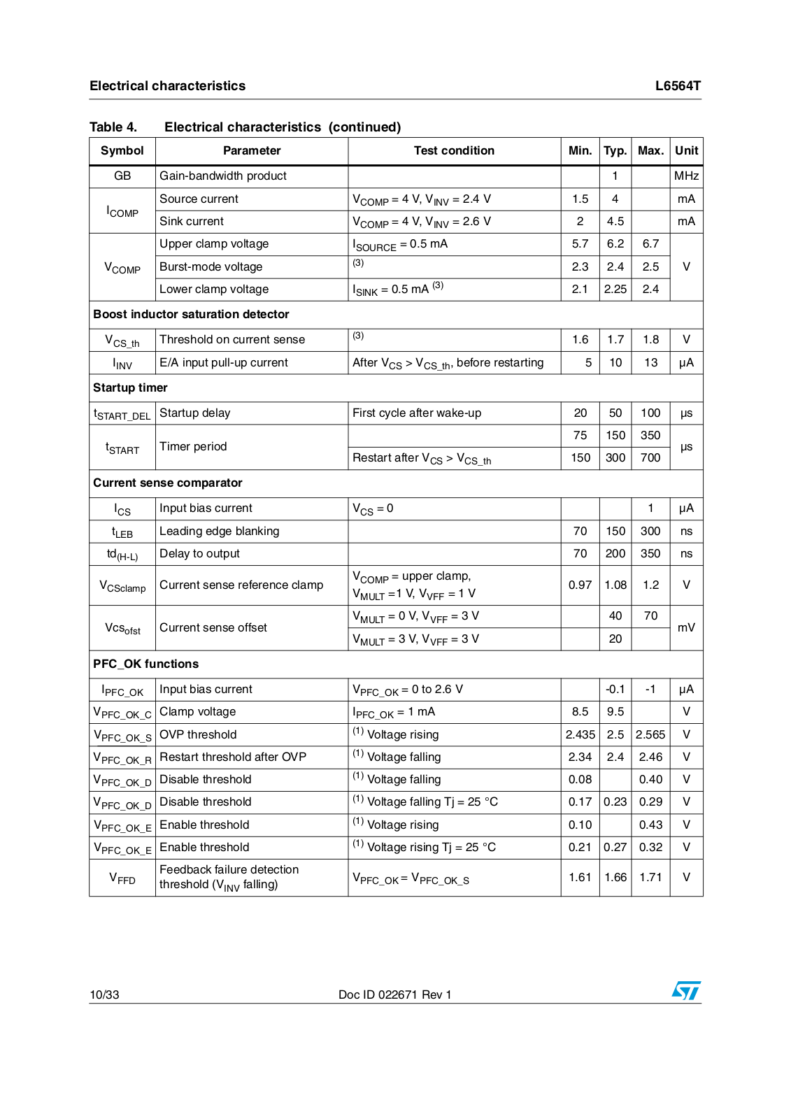
Page 10
Page 11
Page 12
Page 13
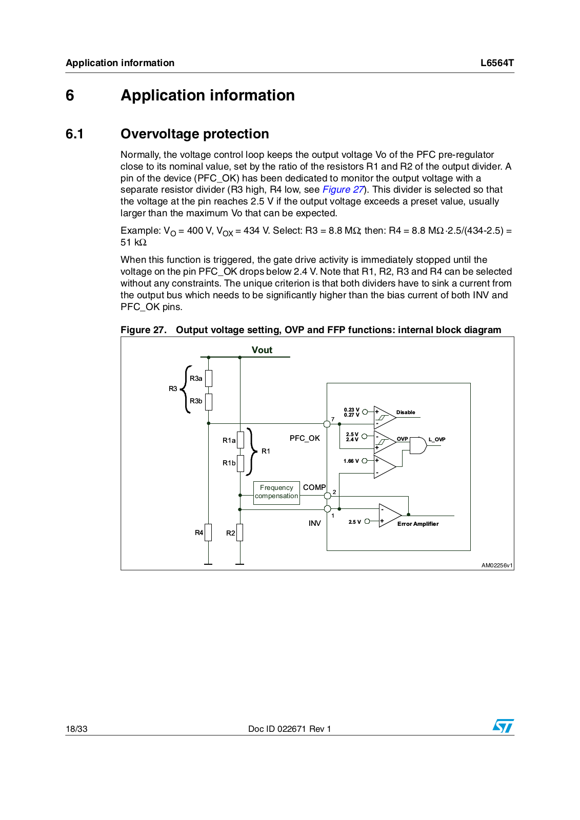
Page 14
Page 15
Page 16
Page 17
Page 18
Page 19
Page 20
Page 21
Page 22
Page 23
Page 24
Page 25
Page 26
Page 27
Page 28
Page 29
Page 30
Page 31
Page 32
Page 33
 Loading...


")