


ST L6563, L6563A User Manual

现货库存、技术资料、百科信息、热点资讯,精彩尽在鼎好!
G
Advanced transition-mode PFC controller
Features
■ Very precise adjustable output overvoltage
protection
■ Tracking boost function
■ Protection against feedback loop failure
(Latched shutdown)
■ Interface for cascaded converter's PWM
controller
■ Input voltage feedforward (1/V
■ Inductor saturation detection (L6563 only)
■ Remote ON/OFF control
■ Low (≤ 90µA) start-up current
■ 5mA max. quiescent current
■ 1.5% (@ T
= 25°C) internal reference voltage
J
■ -600/+800 mA totem pole gate driver with
active pull-down during UVLO
■ SO14 package
Figure 1. Block diagram
TRACKING
BOOST
6
TBO
V
ZCD
RUN
CC
ND
1:1
CURRENT
MIRROR
1:1
BUFFER
3V
14
12
11
1.4V
0.7V
10
-
+
0.52V
0.6V
ON/OFF CONTROL
(BROWNOUT DETECTION)
2
)
INV COMP MULT
123
-
+
2.5V
VOLT AGE
from
REGULATOR
VFF
ZERO CURRENT
-
+
R2
DETECTOR
(I NTERNA L SU PPLY BUS)
R1
CO MPAR ATOR
+
-
VREF2
9
PWM_STOP
references
Vbi a s
UVLO
Voltage
DISABLE
L6563A
SO-14
Applications
PFC pre-regulators for:
■ HI-END AC-DC adapter/charger
■ Desktop PC, server, WEB server
■ IEC61000-3-2 OR JEIDA-MITI compliant
SMPS, in excess of 350W
Table 1. Device summary
Part number Package Packaging
L6563 SO-14 Tube
L6563TR SO-14 Tape & Reel
L6563A SO-14 Tube
L6563ATR SO-14 Tape & Reel
VFF
MUL TIP LI ER
UVLO
Idea l diod e
+-
INDUCTOR
SATURATION
DETECTION
( not in L6563A )
RSQ
PWM_LATCH
5
LI NE VOLT AGE
FEEDFOR WARD
1.7V
Starter
STARTER
LATCH
Vbi as
8
OFF
1 / V
LEADIN G-EDGE
+-
Q
SAT
15 V
Driver
SAT
FEEDBACK
FAILURE
PROTEC TION
2
BLANKING
+
4
CS
VCC
13
GD
0.2V
0.26V
+
PFC_OK
7
-
2.5V
L6563
March 2007 Rev 4 1/39
www.st.com
39

Contents L6563 - L6563A
Contents
1 Description . . . . . . . . . . . . . . . . . . . . . . . . . . . . . . . . . . . . . . . . . . . . . . . . . 3
1.1 Pin connection . . . . . . . . . . . . . . . . . . . . . . . . . . . . . . . . . . . . . . . . . . . . . . 4
1.2 Pin description . . . . . . . . . . . . . . . . . . . . . . . . . . . . . . . . . . . . . . . . . . . . . . 4
2 Absolute maximum ratings . . . . . . . . . . . . . . . . . . . . . . . . . . . . . . . . . . . 6
3 Thermal data . . . . . . . . . . . . . . . . . . . . . . . . . . . . . . . . . . . . . . . . . . . . . . . 6
4 Electrical characteristics . . . . . . . . . . . . . . . . . . . . . . . . . . . . . . . . . . . . . 7
5 Typical electrical performance . . . . . . . . . . . . . . . . . . . . . . . . . . . . . . . . 11
6 Application information . . . . . . . . . . . . . . . . . . . . . . . . . . . . . . . . . . . . . 16
6.1 Overvoltage protection . . . . . . . . . . . . . . . . . . . . . . . . . . . . . . . . . . . . . . . 16
6.2 Feedback Failure Protection (FFP) . . . . . . . . . . . . . . . . . . . . . . . . . . . . . 18
6.3 Voltage Feedforward . . . . . . . . . . . . . . . . . . . . . . . . . . . . . . . . . . . . . . . . 18
6.4 THD optimizer circuit . . . . . . . . . . . . . . . . . . . . . . . . . . . . . . . . . . . . . . . . 21
6.5 Tracking Boost function . . . . . . . . . . . . . . . . . . . . . . . . . . . . . . . . . . . . . . 23
6.6 Inductor saturation detection (L6563 only) . . . . . . . . . . . . . . . . . . . . . . . . 27
6.7 Power management/housekeeping functions . . . . . . . . . . . . . . . . . . . . . . 28
6.8 Summary of L6563/A idle states . . . . . . . . . . . . . . . . . . . . . . . . . . . . . . . 31
7 Application examples and ideas . . . . . . . . . . . . . . . . . . . . . . . . . . . . . . 32
8 Package mechanical data . . . . . . . . . . . . . . . . . . . . . . . . . . . . . . . . . . . . 37
9 Revision history . . . . . . . . . . . . . . . . . . . . . . . . . . . . . . . . . . . . . . . . . . . 38
2/39
L6563 - L6563A Description
1 Description
The device is a current-mode PFC controller operating in Transition Mode (TM). Based on
the core of a standard TM PFC controller, it offers improved performance and additional
functions.
The highly linear multiplier, along with a special correction circuit that reduces crossover
distortion of the mains current, allows wide-range-mains operation with an extremely low
THD even over a large load range.
The output voltage is controlled by means of a voltage-mode error amplifier and a precise
(1.5% @T
response to sudden mains voltage changes are improved by the voltage feedforward
function (1/V
Additionally, the IC provides the option for tracking boost operation (where the output
voltage is changed tracking the mains voltage). The device features extremely low
consumption (≤ 90 µA before start-up and ≤ 5 mA running).
In addition to an effective two-step OVP that handles normal operation overvoltages, the IC
provides also a protection against feedback loop failures or erroneous output voltage
setting.
In the L6563 a protection is added to stop the PFC stage in case the boost inductor
saturates. This function is not included in the L6563A. This is the only difference between
the two part numbers.
An interface with the PWM controller of the DC-DC converter supplied by the PFC preregulator is provided: the purpose is to stop the operation of the converter in case of
anomalous conditions for the PFC stage (feedback loop failure, boost inductor's core
saturation) in the L6563 only and to disable the PFC stage in case of light load for the DCDC converter, so as to make it easier to comply with energy saving norms (Blue Angel,
EnergyStar, Energy2000, etc.). The device includes disable functions suitable for remote
ON/OFF control both in systems where the PFC pre-regulator works as a master and in
those where it works as a slave.
The totem-pole output stage, capable of 600 mA source and 800 mA sink current, is suitable
to drive high current MOSFETs or IGBTs. This, combined with the other features and the
possibility to operate with the proprietary Fixed-Off-Time control, makes the device an
excellent low-cost solution for EN61000-3-2 compliant SMPS in excess of 350W.
= 25°C) internal voltage reference. The stability of the loop and the transient
J
2
correction).
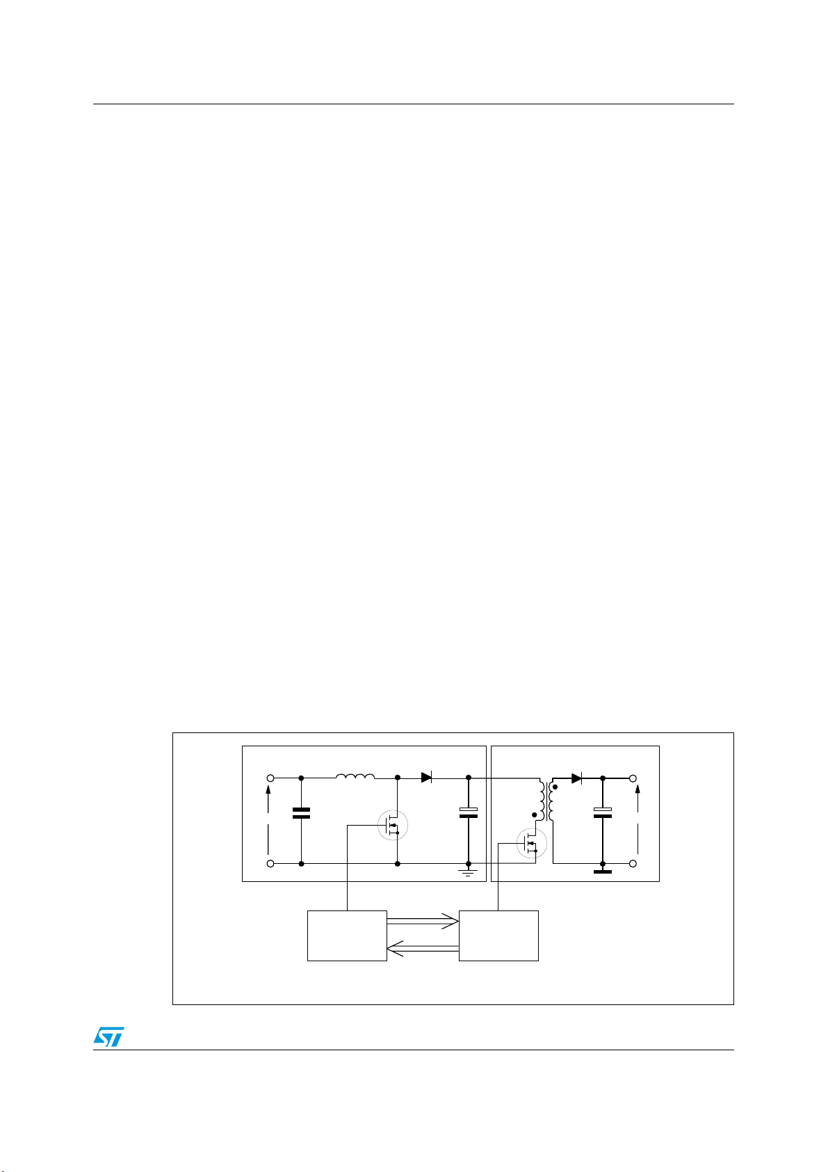
Figure 2. Typical system block diagram
PFC PRE-REGULATOR
V
inac
PWM is turned off in case of PFC’s
anomalous operation for safety
L6563
L6563A
PFC can be turned off at light
load to ease compliance with
energy saving regulations.
3/39
DC-DC CONVERTER
PWM or
Resonant
CONTROLLER
V
outdc
Description L6563 - L6563A
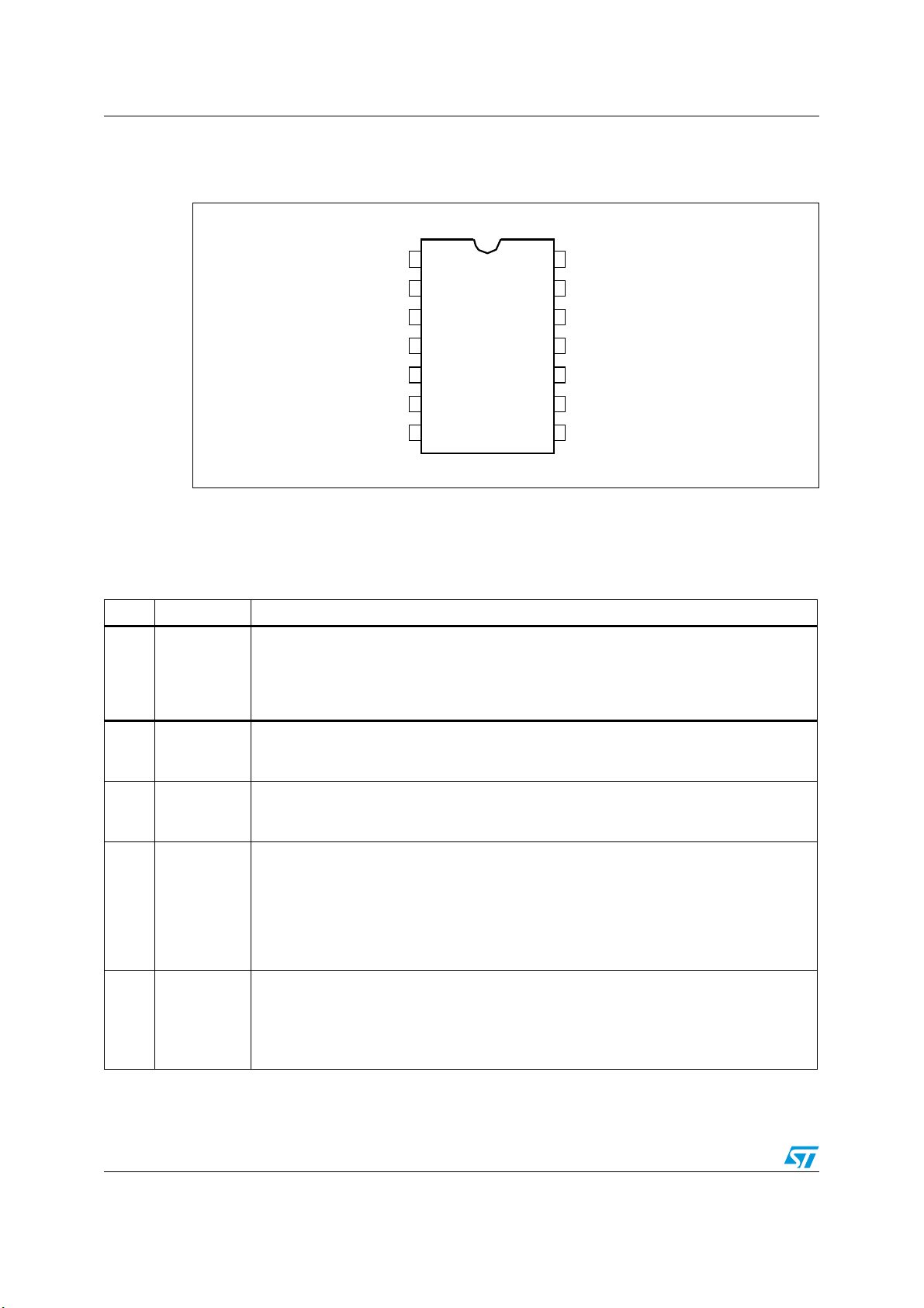
1.1 Pin connection
Figure 3. Pin connection (top view)
INV
COMP
MULT
CS
VFF
TBO
PFC_OK
1
2
3
4
5
6
7
14
13
12
11
10
9
8
1.2 Pin description
Table 2. Pin description
Pin N° Name Description
Inverting input of the error amplifier. The information on the output voltage of the PFC preregulator is fed into the pin through a resistor divider.
1INV
2COMP
3MULT
4CS
5VFF
The pin normally features high impedance but, if the tracking boost function is used, an
internal current generator programmed by TBO (pin 6) is activated. It sinks current from the
pin to change the output voltage so that it tracks the mains voltage.
Output of the error amplifier. A compensation network is placed between this pin and INV
(pin 1) to achieve stability of the voltage control loop and ensure high power factor and low
THD.
Main input to the multiplier. This pin is connected to the rectified mains voltage via a
resistor divider and provides the sinusoidal reference to the current loop. The voltage on
this pin is used also to derive the information on the RMS mains voltage.
Input to the PWM comparator. The current flowing in the MOSFET is sensed through a
resistor, the resulting voltage is applied to this pin and compared with an internal reference
to determine MOSFET’s turn-off.
A second comparison level at 1.7V detects abnormal currents (e.g. due to boost inductor
saturation) and, on this occurrence, shuts down the IC, reduces its consumption almost to
the start-up level and asserts PWM_LATCH (pin 8) high. This function is not present in the
L6563A.
2
Second input to the multiplier for 1/V
connected from the pin to GND. They complete the internal peak-holding circuit that
derives the information on the RMS mains voltage. The voltage at this pin, a DC level equal
to the peak voltage at pin MULT (pin 3), compensates the control loop gain dependence on
the mains voltage. Never connect the pin directly to GND.
function. A capacitor and a parallel resistor must be
Vcc
GD
GND
ZCD
RUN
PWM_STOP
PWM_LATCH
4/39

L6563 - L6563A Description
Table 2. Pin description (continued)
Pin N° Name Description
Tracking Boost function. This pin provides a buffered VFF voltage. A resistor connected
6TBO
7PFC_OK
8PWM_LATCH
9PWM_STOP
between this pin and GND defines a current that is sunk from pin INV (pin 1). In this way,
the output voltage is changed proportionally to the mains voltage (tracking boost). If this
function is not used leave this pin open.
PFC pre-regulator output voltage monitoring/disable function. This pin senses the output
voltage of the PFC pre-regulator through a resistor divider and is used for protection
purposes. If the voltage at the pin exceeds 2.5V the IC is shut down, its consumption goes
almost to the start-up level and this condition is latched. PWM_LATCH pin is asserted high.
Normal operation can be resumed only by cycling the Vcc. This function is used for
protection in case the feedback loop fails.
If the voltage on this pin is brought below 0.2V the IC is shut down and its consumption is
considerably reduced. To restart the IC the voltage on the pin must go above 0.26V. If these
functions are not needed, tie the pin to a voltage between 0.26 and 2.5 V.
Output pin for fault signaling. During normal operation this pin features high impedance. If
either a voltage above 2.5V at PFC_OK (pin 7) or a voltage above 1.7V on CS (pin 4) of
L6563 is detected the pin is asserted high. Normally, this pin is used to stop the operation
of the DC-DC converter supplied by the PFC pre-regulator by invoking a latched disable of
its PWM controller. If not used, the pin will be left floating.
Output pin for fault signaling. During normal operation this pin features high impedance. If
the IC is disabled by a voltage below 0.5V on RUN (pin 10) the voltage at the pin is pulled
to ground. Normally, this pin is used to temporarily stop the operation of the DC-DC
converter supplied by the PFC pre-regulator by disabling its PWM controller. If not used,
the pin will be left floating.
Remote ON/OFF control. A voltage below 0.52V shuts down (not latched) the IC and
brings its consumption to a considerably lower level. PWM_STOP is asserted low. The IC
10 RUN
11 ZCD
12 GND Ground. Current return for both the signal part of the IC and the gate driver.
13 GD
14 VCC Supply Voltage of both the signal part of the IC and the gate driver.
restarts as the voltage at the pin goes above 0.6V. Connect this pin to VFF (pin 5) either
directly or through a resistor divider to use this function as brownout (AC mains
undervoltage) protection, tie to INV (pin 1) if the function is not used.
Boost inductor’s demagnetization sensing input for transition-mode operation. A negativegoing edge triggers MOSFET’s turn-on.
Gate driver output. The totem pole output stage is able to drive power MOSFET’s and
IGBT’s with a peak current of 600 mA source and 800 mA sink. The high-level voltage of
this pin is clamped at about 12V to avoid excessive gate voltages.
5/39
Absolute maximum ratings L6563 - L6563A
2 Absolute maximum ratings
Table 3. Absolute maximum ratings
Symbol Pin Parameter Value Unit
V
CC
---
--- 1, 3, 7
I
PWM_STOP
I
ZCD
P
TOT
T
J
T
STG
14 IC supply voltage (Icc = 20mA) self-limited V
2, 4 to 6, 8
to 10
10 Max. sink current 3 mA
Analog inputs & outputs -0.3 to 8 V
Max. pin voltage (I
9 Zero current detector max. current
Power dissipation @TA = 50°C
Junction temperature operating range -25 to 150 °C
Storage temperature -55 to 150 °C
= 1 mA)
pin
Self-limited V
-10 (source)
10 (sink)
0.75 W
mA
3 Thermal data
Table 4. Thermal data
Symbol Parameter Value Unit
R
thJA
Maximum thermal resistance junction-ambient 120 °C/W
6/39

L6563 - L6563A Electrical characteristics
4 Electrical characteristics
Table 5. Electrical characteristics
( -25°C < T
and GND; unless otherwise specified)
Symbol Parameter Test condition Min Typ Max Unit
Supply voltage
Vcc Operating range After turn-on 10.3 22 V
Vcc
Vcc
Hys Hysteresis 2.3 2.7 V
V
Supply current
< +125°C, VCC = 12V, Co = 1nF between pin GD and GND, CFF =1µF between pin VFF
J
Turn-on threshold
On
Turn-off threshold
Off
Zener Voltage Icc = 20 mA 22 25 28 V
Z
(1)
(1)
11 12 13 V
8.7 9.5 10.3 V
I
start-up
I
I
CC
I
qdis
I
Start-up current Before turn-on, Vcc = 10V 50 90 µA
Quiescent current After turn-on 3 5 mA
q
Operating supply current @ 70kHz 3.8 5.5 mA
Idle state quiescent
Current
Quiescent current During static/dynamic OVP 2 3 mA
q
Multiplier input
I
MULT
V
MULT
V
CLAMP
Vcs∆
---------------------
V
∆
MULT
K
Input bias current
Linear operation range 0 to 3 V
Internal clamp level
Output max. slope
Gain
M
Error amplifier
(3)
Latched by PFC_OK > Vthl or
Vcs > V
CSdis
Disabled by PFC_OK < Vth or
RUN < V
V
I
MULT
V
V
V
V
DIS
= 0 to 3 V
MULT
= 1 mA
=0 to 0.5V, VFF=0.8V
MULT
= Upper clamp
COMP
= 1 V, V
MULT
VFF
= V
COMP
MULT
= 4 V,
180 250 µA
1.5 2.2 mA
-0.2 -1 µA
99.5 V
2.2 2.34 V/V
0.375 0.45 0.525 V
V
I
INV
INV
Voltage feedback input
threshold
TJ = 25 °C
10.3 V < Vcc < 22 V
(2)
2.465 2.5 2.535
V
2.44 2.56
Line regulation Vcc = 10.3 V to 22V 2 5 mV
Input bias current
TBO open, V
= 0 to 4 V
INV
-0.2 -1 µA
7/39

Electrical characteristics L6563 - L6563A
Table 5. Electrical characteristics (continued)
( -25°C < T
< +125°C, VCC = 12V, Co = 1nF between pin GD and GND, CFF =1µF between pin VFF
J
and GND; unless otherwise specified)
Symbol Parameter Test condition Min Typ Max Unit
V
INVCLAMP
Internal clamp level
I
INV
= 1 mA
99.5 V
Gv Voltage gain Open loop 60 80 dB
GB Gain-bandwidth product 1 MHz
I
COMP
V
COMP
Source current
Sink current
Upper clamp voltage
Lower clamp voltage
V
COMP
V
COMP
I
SOURCE
I
= 0.5 mA
SINK
= 4V, V
= 4V, V
= 0.5 mA
INV
INV
(2)
= 2.4 V
= 2.6 V
-2 -3.5 -5 mA
2.5 4.5 mA
5.7 6.2 6.7 V
2.12.252.4 V
Current sense comparator
I
CS
t
LEB
td
(H-L)
V
CSclamp
Vcs
V
CSdis
Input bias current
Leading edge blanking 100 200 300 ns
Delay to output 120 ns
Current sense reference
clamp
Current sense offset
offset
Ic latch-off level (L6563
only)
V
= 0
CS
V
= Upper clamp,
COMP
= V
V
VFF
V
= 0, V
MULT
V
= 3V, V
MULT
(2)
MULT
=0.5V
= 3V
VFF
VFF
= 3V
-1 µA
1.0 1.08 1.16 V
25
5
1.6 1.7 1.8 V
mV
Output overvoltage
I
OVP
Dynamic OVP triggering
current
Hys Hysteresis
Static OVP threshold
Voltage feedforward
V
VFF
∆V
Linear operation range
Dropout
V
MULTpk-VVFF
(4)
(2)
R
= 47 kΩ to GND
FF
17 20 23 µA
15 µA
2 2.15 2.3 V
0.5 3 V
20 mV
8/39

L6563 - L6563A Electrical characteristics
Table 5. Electrical characteristics (continued)
( -25°C < T
< +125°C, VCC = 12V, Co = 1nF between pin GD and GND, CFF =1µF between pin VFF
J
and GND; unless otherwise specified)
Symbol Parameter Test condition Min Typ Max Unit
Zero current detector
V
ZCDH
V
ZCDL
V
ZCDA
V
ZCDT
I
ZCDb
I
ZCDsrc
I
ZCDsnk
Upper clamp voltage
Lower clamp voltage
Arming voltage
(positive-going edge)
Triggering voltage
(negative-going edge)
Input bias current
Source current capability -2.5 mA
Sink current capability 2.5 mA
Tracking boost function
∆V
I
TBO
Dropout voltage
V
- V
VFF
TBO
Linear operation 0 0.25 mA
I
- I
TBO
current
INV
mismatch
V
TBOclamp
Clamp voltage
PFC_OK
V
V
V
EN
I
PFC_OK
V
clamp
Latch-off threshold
thl
Disable threshold
th
Enable threshold
Input bias current
Clamp voltage
I
= 2.5 mA
ZCD
I
= - 2.5 mA
ZCD
(4)
(4)
= 1 to 4.5 V
V
ZCD
I
= 0.25 mA
TBO
= 25 µA to 0.25 mA
I
TBO
(2)
= 4V
V
VFF
Voltage rising
Voltage falling
Voltage rising
V
PFC_OK
I
PFC_OK
(2)
= 0 to 2.5V
= 1 mA
(2)
(2)
5.0 5.7 V
-0.3 0 0.3 V
1.4 V
0.7 V
1µA
20 mV
-3.5 3.5 %
2.9 3 3.1 V
2.4 2.5 2.6 V
0.2 V
0.26 V
-0.1 -1 µA
99.5 V
PWM_LATCH
I
leak
V
H
PWM_STOP
I
leak
V
L
V
clamp
Low level leakage
current
High level
High level leakage
current
Low level
Clamp voltage
V
PWM_LATCH
I
PWM_LATCH
V
PWM_STOP
I
PWM_STOP
PFC_OK
= 2 mA
I
=0
= -0.5 mA
3.7 V
= 6V
= 0.5 mA
99.5 V
9/39
-1 µA
1µA
1V
Electrical characteristics L6563 - L6563A
Table 5. Electrical characteristics (continued)
( -25°C < T
< +125°C, VCC = 12V, Co = 1nF between pin GD and GND, CFF =1µF between pin VFF
J
and GND; unless otherwise specified)
Symbol Parameter Test condition Min Typ Max Unit
Run function
I
RUN
V
DIS
V
EN
Start timer
t
START
Gate driver
V
OHdrop
V
OLdrop
t
f
t
r
V
Oclamp
V
Input bias current
Disable threshold
Enable threshold
= 0 to 3 V
RUN
Voltage falling
Voltage rising
(2)
(2)
-1 µA
0.5 0.52 0.54 V
0.56 0.6 0.64 V
Start timer period 75 150 300 µs
Dropout voltage
I
GDsource
I
GDsource
I
GDsink
= 20 mA
= 200 mA
= 200 mA
22.6V
2.5 3 V
12V
Current fall time 30 70 ns
Current rise time 40 80 ns
Output clamp voltage
UVLO saturation
(1), (2) Parameters tracking each other
(3) The multiplier output is given by:
(4) Parameters guaranteed by design, functionality tested in production.
I
GDsource
Vcc=0 to Vcc
= 5mA; Vcc = 20V
, I
=10mA
On
sink
V
------------------------------------------------------------ -
V
CSKM
⋅=
MULTVCOMP
V
2
VFF
10 12 15 V
1.1 V
2.5–()⋅
10/39
L6563 - L6563A Typical electrical performance
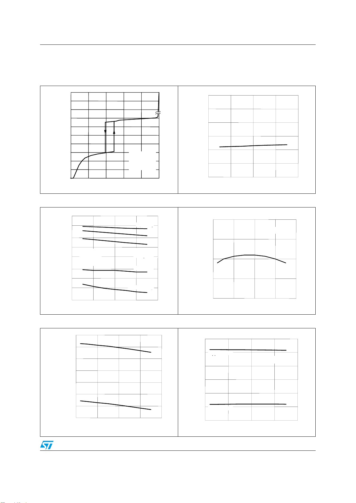
5 Typical electrical performance
Figure 4. Supply current vs supply voltage Figure 5. V
z (pin 14)
z (pin 14)
Vcc
Icc
Icc
(mA)
(mA)
10
10
5
5
1
1
0.5
0.5
0.1
0.1
0.05
0.05
0.01
0.01
0.005
0.005
0
0
0 5 10 15 20
0 5 10 15 20
Vcc(V)
Vcc(V)
Figure 6. IC consumption vs T
Icc
Icc
10
10
(mA)
(mA)
5
5
2
2
1
1
Vcc = 12 V
Vcc = 12 V
0.5
0.5
Co = 1 nF
Co = 1 nF
f = 70 kHz
f = 70 kHz
0.2
0.2
0.1
0.1
0.05
0.05
Co = 1nF
Co = 1nF
f = 70 kHz
f = 70 kHz
j
j
= 25°C
= 25°C
T
T
J
Operating
Operating
Quiescent
Quiescent
Disabled or
Disabled or
during OVP
during OVP
Latched off
Latched off
Before start-up
Before start-up
25
25
Vcc
(V)
(V)
28
28
27
27
26
26
25
25
24
24
23
23
22
22
-50 0 50 100 150
-50 0 50 100 150
Figure 7. Feedback reference vs T
V
V
REF
REF
(pin 1)
(pin 1)
(V)
(V)
2.6
2.6
2.55
2.55
2.5
2.5
2.45
2.45
Zener voltage vs T
CC
Tj (°C)
Tj (°C)
J
J
Vcc = 12 V
Vcc = 12 V
0.02
0.02
-50 0 50 100 150
-50 0 50 100 150
Tj (°C)
Tj (°C)
Figure 8. Start-up & UVLO vs T
12.5
12.5
CC-ON
CC-ON
V
V
(V)
(V)
12
12
11.5
11.5
11
11
10.5
10.5
10
10
CC-OFF
CC-OFF
V
V
9.5
9.5
(V)
(V)
9
9
-50 0 50 100 150
-50 0 50 100 150
Tj (°C)
Tj (°C)
2.4
2.4
-50 0 50 100 150
-50 0 50 100 150
Tj (°C)
Tj (°C)
J
Figure 9. E/A output clamp levels vs T
V
V
COMP
COMP
(pin 2)
(pin 2)
7
7
(V)
(V)
6
6
Upper clamp
Upper clamp
Vcc = 12 V
Vcc = 12 V
5
5
4
4
3
3
2
2
Lower clamp
Lower clamp
1
1
-50 0 50 100 150
-50 0 50 100 150
Tj (°C)
Tj (°C)
J
11/39
Typical electrical performance L6563 - L6563A
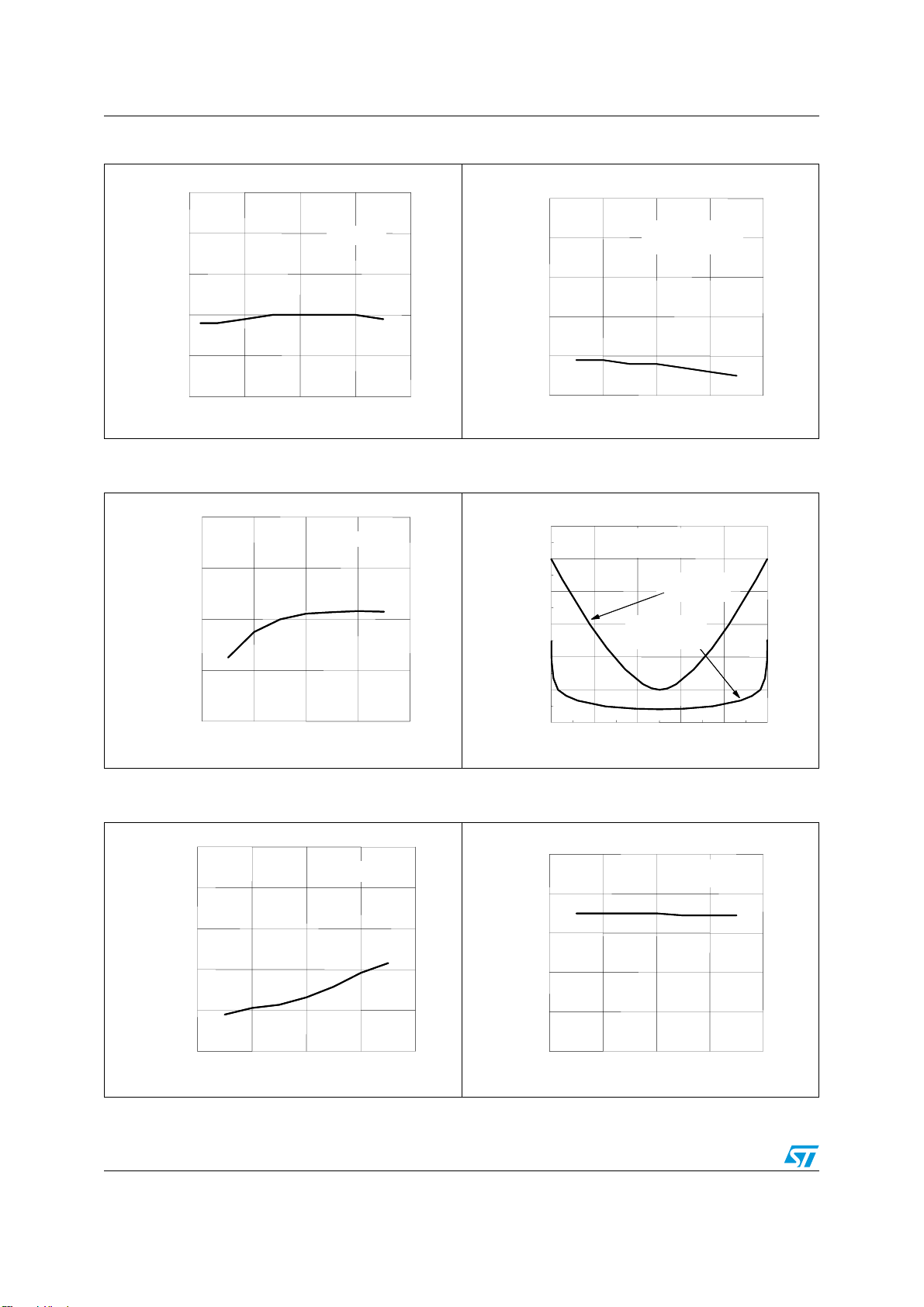
Figure 10. Static OVP level vs T
V
V
COMP
COMP
(pin 2)
(pin 2)
2.5
2.5
(V)
(V)
2.4
2.4
2.3
2.3
2.2
2.2
2.1
2.1
2
2
-50 0 50 100 150
-50 0 50 100 150
Tj (°C)
Tj (°C)
J
Vcc = 12 V
Vcc = 12 V
Figure 12. Dynamic OVP current vs TJ
(normalized value)
I
I
OVP
OVP
120%
120%
Vcc = 12 V
Vcc = 12 V
110%
110%
Figure 11. Vcs clamp vs T
V
V
CSx (pin 4)
CSx (pin 4)
(V)
(V)
1.5
1.5
1.4
1.4
1.3
1.3
1.2
1.2
1.1
1.1
1
1
-50 0 50 100 150
-50 0 50 100 150
V
V
COMP
COMP
Tj (°C)
Tj (°C)
J
Vcc = 12 V
Vcc = 12 V
= Upper clamp
= Upper clamp
Figure 13. Current-sense offset vs
mains voltage phase angle
V
V
CSoffset (pin 4)
CSoffset (pin 4)
30
30
(mV)
(mV)
25
25
20
20
Vcc = 12 V
Vcc = 12 V
Tj = 25 °
Tj = 25 °
V
V
MULT
MULT
V
V
FF
FF
= 0 to 3V
= 0 to 3V
= 3V
= 3V
100%
100%
90%
90%
80%
80%
-50 0 50 100 150
-50 0 50 100 150
Tj (°C)
Tj (°C)
Figure 14. Delay-to-output vs T
t
t
D(H-L)
D(H-L)
300
300
(ns)
(ns)
250
250
200
200
150
150
100
100
50
50
-50 0 50 100 150
-50 0 50 100 150
Tj (°C)
Tj (°C)
J
Vcc = 12 V
Vcc = 12 V
15
15
10
10
5
5
0
0
0 0.628 1.256 1.884 2.512 3.14
0 0.628 1.256 1.884 2.512 3.14
V
V
MULT
MULT
V
V
= 0 to 0.7V
= 0 to 0.7V
= 0.7V
= 0.7V
FF
FF
θ(
θ(
°)
°)
Figure 15. Ic latch-off level on current sense vs
T
(L6563 only)
J
Vpin4
Vpin4
2.0
2.0
(V)
(V)
1.8
1.8
1.6
1.6
1.4
1.4
1.2
1.2
1.0
1.0
-50 0 50 100 150
-50 0 50 100 150
Tj (°C)
Tj (°C)
Vcc = 12 V
Vcc = 12 V
12/39