


现货库存、技术资料、百科信息、热点资讯,精彩尽在鼎好!
G
Advanced transition-mode PFC controller
Features
■ Very precise adjustable output overvoltage
protection
■ Tracking boost function
■ Protection against feedback loop failure
(Latched shutdown)
■ Interface for cascaded converter's PWM
controller
■ Input voltage feedforward (1/V
■ Inductor saturation detection (L6563 only)
■ Remote ON/OFF control
■ Low (≤ 90µA) start-up current
■ 5mA max. quiescent current
■ 1.5% (@ T
= 25°C) internal reference voltage
J
■ -600/+800 mA totem pole gate driver with
active pull-down during UVLO
■ SO14 package
Figure 1. Block diagram
TRACKING
BOOST
6
TBO
V
ZCD
RUN
CC
ND
1:1
CURRENT
MIRROR
1:1
BUFFER
3V
14
12
11
1.4V
0.7V
10
-
+
0.52V
0.6V
ON/OFF CONTROL
(BROWNOUT DETECTION)
2
)
INV COMP MULT
123
-
+
2.5V
VOLT AGE
from
REGULATOR
VFF
ZERO CURRENT
-
+
R2
DETECTOR
(I NTERNA L SU PPLY BUS)
R1
CO MPAR ATOR
+
-
VREF2
9
PWM_STOP
references
Vbi a s
UVLO
Voltage
DISABLE
L6563A
SO-14
Applications
PFC pre-regulators for:
■ HI-END AC-DC adapter/charger
■ Desktop PC, server, WEB server
■ IEC61000-3-2 OR JEIDA-MITI compliant
SMPS, in excess of 350W
Table 1. Device summary
Part number Package Packaging
L6563 SO-14 Tube
L6563TR SO-14 Tape & Reel
L6563A SO-14 Tube
L6563ATR SO-14 Tape & Reel
VFF
MUL TIP LI ER
UVLO
Idea l diod e
+-
INDUCTOR
SATURATION
DETECTION
( not in L6563A )
RSQ
PWM_LATCH
5
LI NE VOLT AGE
FEEDFOR WARD
1.7V
Starter
STARTER
LATCH
Vbi as
8
OFF
1 / V
LEADIN G-EDGE
+-
Q
SAT
15 V
Driver
SAT
FEEDBACK
FAILURE
PROTEC TION
2
BLANKING
+
4
CS
VCC
13
GD
0.2V
0.26V
+
PFC_OK
7
-
2.5V
L6563
March 2007 Rev 4 1/39
www.st.com
39

Contents L6563 - L6563A
Contents
1 Description . . . . . . . . . . . . . . . . . . . . . . . . . . . . . . . . . . . . . . . . . . . . . . . . . 3
1.1 Pin connection . . . . . . . . . . . . . . . . . . . . . . . . . . . . . . . . . . . . . . . . . . . . . . 4
1.2 Pin description . . . . . . . . . . . . . . . . . . . . . . . . . . . . . . . . . . . . . . . . . . . . . . 4
2 Absolute maximum ratings . . . . . . . . . . . . . . . . . . . . . . . . . . . . . . . . . . . 6
3 Thermal data . . . . . . . . . . . . . . . . . . . . . . . . . . . . . . . . . . . . . . . . . . . . . . . 6
4 Electrical characteristics . . . . . . . . . . . . . . . . . . . . . . . . . . . . . . . . . . . . . 7
5 Typical electrical performance . . . . . . . . . . . . . . . . . . . . . . . . . . . . . . . . 11
6 Application information . . . . . . . . . . . . . . . . . . . . . . . . . . . . . . . . . . . . . 16
6.1 Overvoltage protection . . . . . . . . . . . . . . . . . . . . . . . . . . . . . . . . . . . . . . . 16
6.2 Feedback Failure Protection (FFP) . . . . . . . . . . . . . . . . . . . . . . . . . . . . . 18
6.3 Voltage Feedforward . . . . . . . . . . . . . . . . . . . . . . . . . . . . . . . . . . . . . . . . 18
6.4 THD optimizer circuit . . . . . . . . . . . . . . . . . . . . . . . . . . . . . . . . . . . . . . . . 21
6.5 Tracking Boost function . . . . . . . . . . . . . . . . . . . . . . . . . . . . . . . . . . . . . . 23
6.6 Inductor saturation detection (L6563 only) . . . . . . . . . . . . . . . . . . . . . . . . 27
6.7 Power management/housekeeping functions . . . . . . . . . . . . . . . . . . . . . . 28
6.8 Summary of L6563/A idle states . . . . . . . . . . . . . . . . . . . . . . . . . . . . . . . 31
7 Application examples and ideas . . . . . . . . . . . . . . . . . . . . . . . . . . . . . . 32
8 Package mechanical data . . . . . . . . . . . . . . . . . . . . . . . . . . . . . . . . . . . . 37
9 Revision history . . . . . . . . . . . . . . . . . . . . . . . . . . . . . . . . . . . . . . . . . . . 38
2/39
L6563 - L6563A Description
1 Description
The device is a current-mode PFC controller operating in Transition Mode (TM). Based on
the core of a standard TM PFC controller, it offers improved performance and additional
functions.
The highly linear multiplier, along with a special correction circuit that reduces crossover
distortion of the mains current, allows wide-range-mains operation with an extremely low
THD even over a large load range.
The output voltage is controlled by means of a voltage-mode error amplifier and a precise
(1.5% @T
response to sudden mains voltage changes are improved by the voltage feedforward
function (1/V
Additionally, the IC provides the option for tracking boost operation (where the output
voltage is changed tracking the mains voltage). The device features extremely low
consumption (≤ 90 µA before start-up and ≤ 5 mA running).
In addition to an effective two-step OVP that handles normal operation overvoltages, the IC
provides also a protection against feedback loop failures or erroneous output voltage
setting.
In the L6563 a protection is added to stop the PFC stage in case the boost inductor
saturates. This function is not included in the L6563A. This is the only difference between
the two part numbers.
An interface with the PWM controller of the DC-DC converter supplied by the PFC preregulator is provided: the purpose is to stop the operation of the converter in case of
anomalous conditions for the PFC stage (feedback loop failure, boost inductor's core
saturation) in the L6563 only and to disable the PFC stage in case of light load for the DCDC converter, so as to make it easier to comply with energy saving norms (Blue Angel,
EnergyStar, Energy2000, etc.). The device includes disable functions suitable for remote
ON/OFF control both in systems where the PFC pre-regulator works as a master and in
those where it works as a slave.
The totem-pole output stage, capable of 600 mA source and 800 mA sink current, is suitable
to drive high current MOSFETs or IGBTs. This, combined with the other features and the
possibility to operate with the proprietary Fixed-Off-Time control, makes the device an
excellent low-cost solution for EN61000-3-2 compliant SMPS in excess of 350W.
= 25°C) internal voltage reference. The stability of the loop and the transient
J
2
correction).
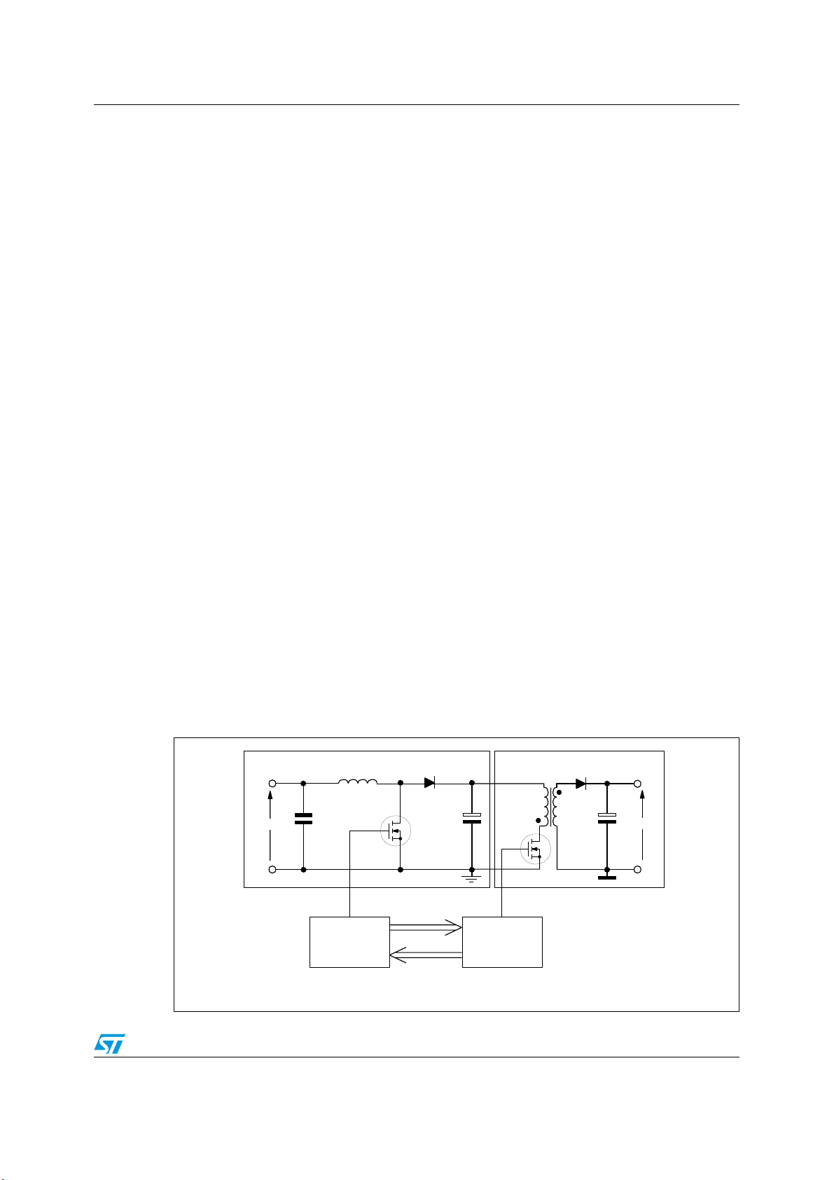
Figure 2. Typical system block diagram
PFC PRE-REGULATOR
V
inac
PWM is turned off in case of PFC’s
anomalous operation for safety
L6563
L6563A
PFC can be turned off at light
load to ease compliance with
energy saving regulations.
3/39
DC-DC CONVERTER
PWM or
Resonant
CONTROLLER
V
outdc
Description L6563 - L6563A
1.1 Pin connection
Figure 3. Pin connection (top view)
INV
COMP
MULT
CS
VFF
TBO
PFC_OK
1
2
3
4
5
6
7
14
13
12
11
10
9
8
1.2 Pin description
Table 2. Pin description
Pin N° Name Description
Inverting input of the error amplifier. The information on the output voltage of the PFC preregulator is fed into the pin through a resistor divider.
1INV
2COMP
3MULT
4CS
5VFF
The pin normally features high impedance but, if the tracking boost function is used, an
internal current generator programmed by TBO (pin 6) is activated. It sinks current from the
pin to change the output voltage so that it tracks the mains voltage.
Output of the error amplifier. A compensation network is placed between this pin and INV
(pin 1) to achieve stability of the voltage control loop and ensure high power factor and low
THD.
Main input to the multiplier. This pin is connected to the rectified mains voltage via a
resistor divider and provides the sinusoidal reference to the current loop. The voltage on
this pin is used also to derive the information on the RMS mains voltage.
Input to the PWM comparator. The current flowing in the MOSFET is sensed through a
resistor, the resulting voltage is applied to this pin and compared with an internal reference
to determine MOSFET’s turn-off.
A second comparison level at 1.7V detects abnormal currents (e.g. due to boost inductor
saturation) and, on this occurrence, shuts down the IC, reduces its consumption almost to
the start-up level and asserts PWM_LATCH (pin 8) high. This function is not present in the
L6563A.
2
Second input to the multiplier for 1/V
connected from the pin to GND. They complete the internal peak-holding circuit that
derives the information on the RMS mains voltage. The voltage at this pin, a DC level equal
to the peak voltage at pin MULT (pin 3), compensates the control loop gain dependence on
the mains voltage. Never connect the pin directly to GND.
function. A capacitor and a parallel resistor must be
Vcc
GD
GND
ZCD
RUN
PWM_STOP
PWM_LATCH
4/39

L6563 - L6563A Description
Table 2. Pin description (continued)
Pin N° Name Description
Tracking Boost function. This pin provides a buffered VFF voltage. A resistor connected
6TBO
7PFC_OK
8PWM_LATCH
9PWM_STOP
between this pin and GND defines a current that is sunk from pin INV (pin 1). In this way,
the output voltage is changed proportionally to the mains voltage (tracking boost). If this
function is not used leave this pin open.
PFC pre-regulator output voltage monitoring/disable function. This pin senses the output
voltage of the PFC pre-regulator through a resistor divider and is used for protection
purposes. If the voltage at the pin exceeds 2.5V the IC is shut down, its consumption goes
almost to the start-up level and this condition is latched. PWM_LATCH pin is asserted high.
Normal operation can be resumed only by cycling the Vcc. This function is used for
protection in case the feedback loop fails.
If the voltage on this pin is brought below 0.2V the IC is shut down and its consumption is
considerably reduced. To restart the IC the voltage on the pin must go above 0.26V. If these
functions are not needed, tie the pin to a voltage between 0.26 and 2.5 V.
Output pin for fault signaling. During normal operation this pin features high impedance. If
either a voltage above 2.5V at PFC_OK (pin 7) or a voltage above 1.7V on CS (pin 4) of
L6563 is detected the pin is asserted high. Normally, this pin is used to stop the operation
of the DC-DC converter supplied by the PFC pre-regulator by invoking a latched disable of
its PWM controller. If not used, the pin will be left floating.
Output pin for fault signaling. During normal operation this pin features high impedance. If
the IC is disabled by a voltage below 0.5V on RUN (pin 10) the voltage at the pin is pulled
to ground. Normally, this pin is used to temporarily stop the operation of the DC-DC
converter supplied by the PFC pre-regulator by disabling its PWM controller. If not used,
the pin will be left floating.
Remote ON/OFF control. A voltage below 0.52V shuts down (not latched) the IC and
brings its consumption to a considerably lower level. PWM_STOP is asserted low. The IC
10 RUN
11 ZCD
12 GND Ground. Current return for both the signal part of the IC and the gate driver.
13 GD
14 VCC Supply Voltage of both the signal part of the IC and the gate driver.
restarts as the voltage at the pin goes above 0.6V. Connect this pin to VFF (pin 5) either
directly or through a resistor divider to use this function as brownout (AC mains
undervoltage) protection, tie to INV (pin 1) if the function is not used.
Boost inductor’s demagnetization sensing input for transition-mode operation. A negativegoing edge triggers MOSFET’s turn-on.
Gate driver output. The totem pole output stage is able to drive power MOSFET’s and
IGBT’s with a peak current of 600 mA source and 800 mA sink. The high-level voltage of
this pin is clamped at about 12V to avoid excessive gate voltages.
5/39

Absolute maximum ratings L6563 - L6563A
2 Absolute maximum ratings
Table 3. Absolute maximum ratings
Symbol Pin Parameter Value Unit
V
CC
---
--- 1, 3, 7
I
PWM_STOP
I
ZCD
P
TOT
T
J
T
STG
14 IC supply voltage (Icc = 20mA) self-limited V
2, 4 to 6, 8
to 10
10 Max. sink current 3 mA
Analog inputs & outputs -0.3 to 8 V
Max. pin voltage (I
9 Zero current detector max. current
Power dissipation @TA = 50°C
Junction temperature operating range -25 to 150 °C
Storage temperature -55 to 150 °C
= 1 mA)
pin
Self-limited V
-10 (source)
10 (sink)
0.75 W
mA
3 Thermal data
Table 4. Thermal data
Symbol Parameter Value Unit
R
thJA
Maximum thermal resistance junction-ambient 120 °C/W
6/39

L6563 - L6563A Electrical characteristics
4 Electrical characteristics
Table 5. Electrical characteristics
( -25°C < T
and GND; unless otherwise specified)
Symbol Parameter Test condition Min Typ Max Unit
Supply voltage
Vcc Operating range After turn-on 10.3 22 V
Vcc
Vcc
Hys Hysteresis 2.3 2.7 V
V
Supply current
< +125°C, VCC = 12V, Co = 1nF between pin GD and GND, CFF =1µF between pin VFF
J
Turn-on threshold
On
Turn-off threshold
Off
Zener Voltage Icc = 20 mA 22 25 28 V
Z
(1)
(1)
11 12 13 V
8.7 9.5 10.3 V
I
start-up
I
I
CC
I
qdis
I
Start-up current Before turn-on, Vcc = 10V 50 90 µA
Quiescent current After turn-on 3 5 mA
q
Operating supply current @ 70kHz 3.8 5.5 mA
Idle state quiescent
Current
Quiescent current During static/dynamic OVP 2 3 mA
q
Multiplier input
I
MULT
V
MULT
V
CLAMP
Vcs∆
---------------------
V
∆
MULT
K
Input bias current
Linear operation range 0 to 3 V
Internal clamp level
Output max. slope
Gain
M
Error amplifier
(3)
Latched by PFC_OK > Vthl or
Vcs > V
CSdis
Disabled by PFC_OK < Vth or
RUN < V
V
I
MULT
V
V
V
V
DIS
= 0 to 3 V
MULT
= 1 mA
=0 to 0.5V, VFF=0.8V
MULT
= Upper clamp
COMP
= 1 V, V
MULT
VFF
= V
COMP
MULT
= 4 V,
180 250 µA
1.5 2.2 mA
-0.2 -1 µA
99.5 V
2.2 2.34 V/V
0.375 0.45 0.525 V
V
I
INV
INV
Voltage feedback input
threshold
TJ = 25 °C
10.3 V < Vcc < 22 V
(2)
2.465 2.5 2.535
V
2.44 2.56
Line regulation Vcc = 10.3 V to 22V 2 5 mV
Input bias current
TBO open, V
= 0 to 4 V
INV
-0.2 -1 µA
7/39

Electrical characteristics L6563 - L6563A
Table 5. Electrical characteristics (continued)
( -25°C < T
< +125°C, VCC = 12V, Co = 1nF between pin GD and GND, CFF =1µF between pin VFF
J
and GND; unless otherwise specified)
Symbol Parameter Test condition Min Typ Max Unit
V
INVCLAMP
Internal clamp level
I
INV
= 1 mA
99.5 V
Gv Voltage gain Open loop 60 80 dB
GB Gain-bandwidth product 1 MHz
I
COMP
V
COMP
Source current
Sink current
Upper clamp voltage
Lower clamp voltage
V
COMP
V
COMP
I
SOURCE
I
= 0.5 mA
SINK
= 4V, V
= 4V, V
= 0.5 mA
INV
INV
(2)
= 2.4 V
= 2.6 V
-2 -3.5 -5 mA
2.5 4.5 mA
5.7 6.2 6.7 V
2.12.252.4 V
Current sense comparator
I
CS
t
LEB
td
(H-L)
V
CSclamp
Vcs
V
CSdis
Input bias current
Leading edge blanking 100 200 300 ns
Delay to output 120 ns
Current sense reference
clamp
Current sense offset
offset
Ic latch-off level (L6563
only)
V
= 0
CS
V
= Upper clamp,
COMP
= V
V
VFF
V
= 0, V
MULT
V
= 3V, V
MULT
(2)
MULT
=0.5V
= 3V
VFF
VFF
= 3V
-1 µA
1.0 1.08 1.16 V
25
5
1.6 1.7 1.8 V
mV
Output overvoltage
I
OVP
Dynamic OVP triggering
current
Hys Hysteresis
Static OVP threshold
Voltage feedforward
V
VFF
∆V
Linear operation range
Dropout
V
MULTpk-VVFF
(4)
(2)
R
= 47 kΩ to GND
FF
17 20 23 µA
15 µA
2 2.15 2.3 V
0.5 3 V
20 mV
8/39

L6563 - L6563A Electrical characteristics
Table 5. Electrical characteristics (continued)
( -25°C < T
< +125°C, VCC = 12V, Co = 1nF between pin GD and GND, CFF =1µF between pin VFF
J
and GND; unless otherwise specified)
Symbol Parameter Test condition Min Typ Max Unit
Zero current detector
V
ZCDH
V
ZCDL
V
ZCDA
V
ZCDT
I
ZCDb
I
ZCDsrc
I
ZCDsnk
Upper clamp voltage
Lower clamp voltage
Arming voltage
(positive-going edge)
Triggering voltage
(negative-going edge)
Input bias current
Source current capability -2.5 mA
Sink current capability 2.5 mA
Tracking boost function
∆V
I
TBO
Dropout voltage
V
- V
VFF
TBO
Linear operation 0 0.25 mA
I
- I
TBO
current
INV
mismatch
V
TBOclamp
Clamp voltage
PFC_OK
V
V
V
EN
I
PFC_OK
V
clamp
Latch-off threshold
thl
Disable threshold
th
Enable threshold
Input bias current
Clamp voltage
I
= 2.5 mA
ZCD
I
= - 2.5 mA
ZCD
(4)
(4)
= 1 to 4.5 V
V
ZCD
I
= 0.25 mA
TBO
= 25 µA to 0.25 mA
I
TBO
(2)
= 4V
V
VFF
Voltage rising
Voltage falling
Voltage rising
V
PFC_OK
I
PFC_OK
(2)
= 0 to 2.5V
= 1 mA
(2)
(2)
5.0 5.7 V
-0.3 0 0.3 V
1.4 V
0.7 V
1µA
20 mV
-3.5 3.5 %
2.9 3 3.1 V
2.4 2.5 2.6 V
0.2 V
0.26 V
-0.1 -1 µA
99.5 V
PWM_LATCH
I
leak
V
H
PWM_STOP
I
leak
V
L
V
clamp
Low level leakage
current
High level
High level leakage
current
Low level
Clamp voltage
V
PWM_LATCH
I
PWM_LATCH
V
PWM_STOP
I
PWM_STOP
PFC_OK
= 2 mA
I
=0
= -0.5 mA
3.7 V
= 6V
= 0.5 mA
99.5 V
9/39
-1 µA
1µA
1V

Electrical characteristics L6563 - L6563A
Table 5. Electrical characteristics (continued)
( -25°C < T
< +125°C, VCC = 12V, Co = 1nF between pin GD and GND, CFF =1µF between pin VFF
J
and GND; unless otherwise specified)
Symbol Parameter Test condition Min Typ Max Unit
Run function
I
RUN
V
DIS
V
EN
Start timer
t
START
Gate driver
V
OHdrop
V
OLdrop
t
f
t
r
V
Oclamp
V
Input bias current
Disable threshold
Enable threshold
= 0 to 3 V
RUN
Voltage falling
Voltage rising
(2)
(2)
-1 µA
0.5 0.52 0.54 V
0.56 0.6 0.64 V
Start timer period 75 150 300 µs
Dropout voltage
I
GDsource
I
GDsource
I
GDsink
= 20 mA
= 200 mA
= 200 mA
22.6V
2.5 3 V
12V
Current fall time 30 70 ns
Current rise time 40 80 ns
Output clamp voltage
UVLO saturation
(1), (2) Parameters tracking each other
(3) The multiplier output is given by:
(4) Parameters guaranteed by design, functionality tested in production.
I
GDsource
Vcc=0 to Vcc
= 5mA; Vcc = 20V
, I
=10mA
On
sink
V
------------------------------------------------------------ -
V
CSKM
⋅=
MULTVCOMP
V
2
VFF
10 12 15 V
1.1 V
2.5–()⋅
10/39
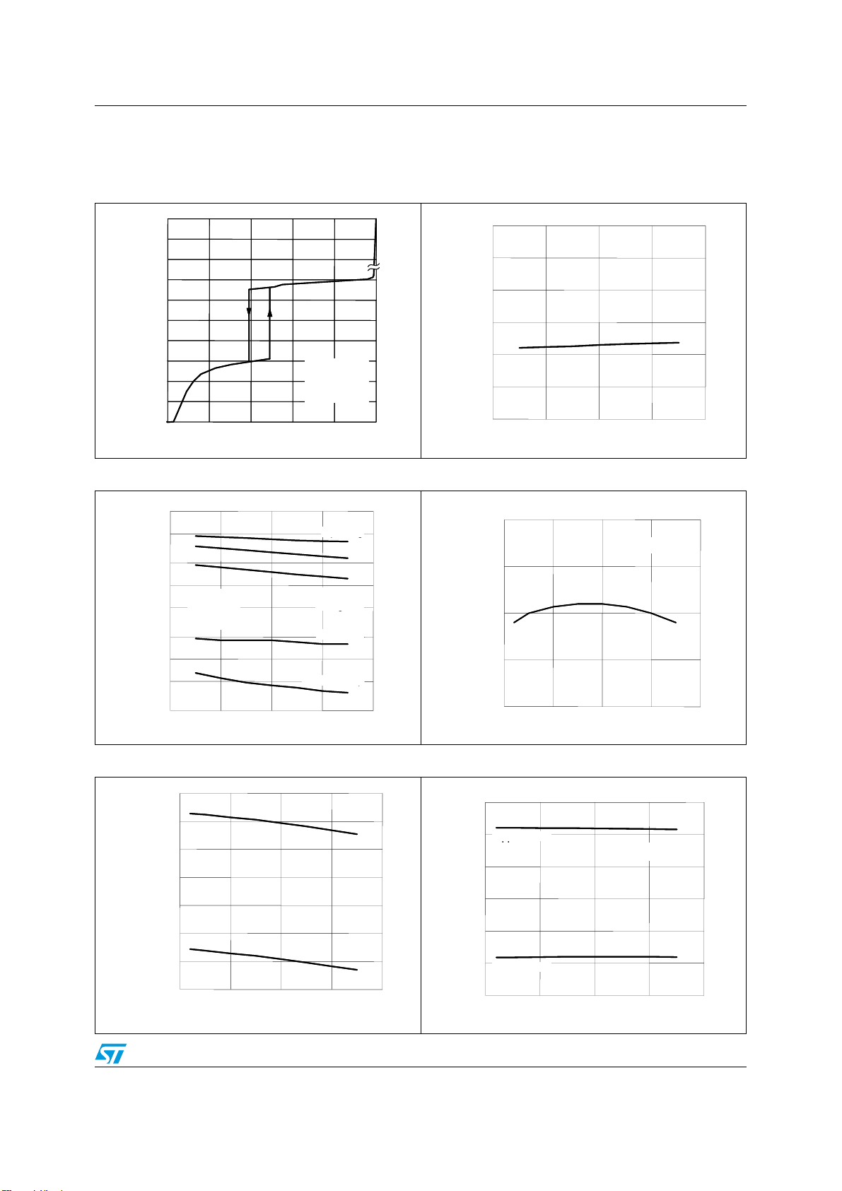
L6563 - L6563A Typical electrical performance
5 Typical electrical performance
Figure 4. Supply current vs supply voltage Figure 5. V
z (pin 14)
z (pin 14)
Vcc
Icc
Icc
(mA)
(mA)
10
10
5
5
1
1
0.5
0.5
0.1
0.1
0.05
0.05
0.01
0.01
0.005
0.005
0
0
0 5 10 15 20
0 5 10 15 20
Vcc(V)
Vcc(V)
Figure 6. IC consumption vs T
Icc
Icc
10
10
(mA)
(mA)
5
5
2
2
1
1
Vcc = 12 V
Vcc = 12 V
0.5
0.5
Co = 1 nF
Co = 1 nF
f = 70 kHz
f = 70 kHz
0.2
0.2
0.1
0.1
0.05
0.05
Co = 1nF
Co = 1nF
f = 70 kHz
f = 70 kHz
j
j
= 25°C
= 25°C
T
T
J
Operating
Operating
Quiescent
Quiescent
Disabled or
Disabled or
during OVP
during OVP
Latched off
Latched off
Before start-up
Before start-up
25
25
Vcc
(V)
(V)
28
28
27
27
26
26
25
25
24
24
23
23
22
22
-50 0 50 100 150
-50 0 50 100 150
Figure 7. Feedback reference vs T
V
V
REF
REF
(pin 1)
(pin 1)
(V)
(V)
2.6
2.6
2.55
2.55
2.5
2.5
2.45
2.45
Zener voltage vs T
CC
Tj (°C)
Tj (°C)
J
J
Vcc = 12 V
Vcc = 12 V
0.02
0.02
-50 0 50 100 150
-50 0 50 100 150
Tj (°C)
Tj (°C)
Figure 8. Start-up & UVLO vs T
12.5
12.5
CC-ON
CC-ON
V
V
(V)
(V)
12
12
11.5
11.5
11
11
10.5
10.5
10
10
CC-OFF
CC-OFF
V
V
9.5
9.5
(V)
(V)
9
9
-50 0 50 100 150
-50 0 50 100 150
Tj (°C)
Tj (°C)
2.4
2.4
-50 0 50 100 150
-50 0 50 100 150
Tj (°C)
Tj (°C)
J
Figure 9. E/A output clamp levels vs T
V
V
COMP
COMP
(pin 2)
(pin 2)
7
7
(V)
(V)
6
6
Upper clamp
Upper clamp
Vcc = 12 V
Vcc = 12 V
5
5
4
4
3
3
2
2
Lower clamp
Lower clamp
1
1
-50 0 50 100 150
-50 0 50 100 150
Tj (°C)
Tj (°C)
J
11/39
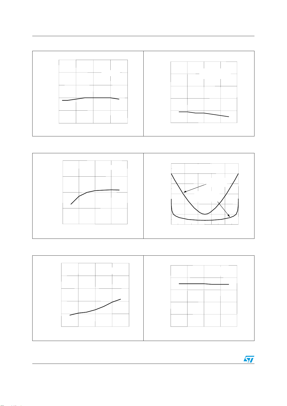
Typical electrical performance L6563 - L6563A
Figure 10. Static OVP level vs T
V
V
COMP
COMP
(pin 2)
(pin 2)
2.5
2.5
(V)
(V)
2.4
2.4
2.3
2.3
2.2
2.2
2.1
2.1
2
2
-50 0 50 100 150
-50 0 50 100 150
Tj (°C)
Tj (°C)
J
Vcc = 12 V
Vcc = 12 V
Figure 12. Dynamic OVP current vs TJ
(normalized value)
I
I
OVP
OVP
120%
120%
Vcc = 12 V
Vcc = 12 V
110%
110%
Figure 11. Vcs clamp vs T
V
V
CSx (pin 4)
CSx (pin 4)
(V)
(V)
1.5
1.5
1.4
1.4
1.3
1.3
1.2
1.2
1.1
1.1
1
1
-50 0 50 100 150
-50 0 50 100 150
V
V
COMP
COMP
Tj (°C)
Tj (°C)
J
Vcc = 12 V
Vcc = 12 V
= Upper clamp
= Upper clamp
Figure 13. Current-sense offset vs
mains voltage phase angle
V
V
CSoffset (pin 4)
CSoffset (pin 4)
30
30
(mV)
(mV)
25
25
20
20
Vcc = 12 V
Vcc = 12 V
Tj = 25 °
Tj = 25 °
V
V
MULT
MULT
V
V
FF
FF
= 0 to 3V
= 0 to 3V
= 3V
= 3V
100%
100%
90%
90%
80%
80%
-50 0 50 100 150
-50 0 50 100 150
Tj (°C)
Tj (°C)
Figure 14. Delay-to-output vs T
t
t
D(H-L)
D(H-L)
300
300
(ns)
(ns)
250
250
200
200
150
150
100
100
50
50
-50 0 50 100 150
-50 0 50 100 150
Tj (°C)
Tj (°C)
J
Vcc = 12 V
Vcc = 12 V
15
15
10
10
5
5
0
0
0 0.628 1.256 1.884 2.512 3.14
0 0.628 1.256 1.884 2.512 3.14
V
V
MULT
MULT
V
V
= 0 to 0.7V
= 0 to 0.7V
= 0.7V
= 0.7V
FF
FF
θ(
θ(
°)
°)
Figure 15. Ic latch-off level on current sense vs
T
(L6563 only)
J
Vpin4
Vpin4
2.0
2.0
(V)
(V)
1.8
1.8
1.6
1.6
1.4
1.4
1.2
1.2
1.0
1.0
-50 0 50 100 150
-50 0 50 100 150
Tj (°C)
Tj (°C)
Vcc = 12 V
Vcc = 12 V
12/39

L6563 - L6563A Typical electrical performance
Figure 16. Multiplier characteristics @ V
V
V
CS
CS
(pin 4)
(pin 4)
(V)
(V)
Vcc = 12 V
Vcc = 12 V
Tj = 25 °C
Tj = 25 °C
1
1
0.8
0.8
0.6
0.6
0.4
0.4
0.2
0.2
0
0
0 0.2 0.4 0.6 0.8 1 1.2
0 0.2 0.4 0.6 0.8 1 1.2
V
V
MULT
MULT
upper voltag e
upper voltag e
clamp
clamp
(pin 3) (V)
(pin 3) (V)
3.5
3.5
3.0
3.0
2.6
2.6
5.5
5.5
5.0
5.0
4.5
4.5
4.0
4.0
V
V
COMP
COMP
= 1V Figure 17. ZCD clamp levels vs T
FF
V
(pin 2)
(pin 2)
(V)
(V)
V
ZCD (pin 11)
ZCD (pin 11)
7
7
(V)
(V)
6
6
5
5
4
4
3
3
2
2
1
1
0
0
-1
-1
-50 0 50 100 150
-50 0 50 100 150
Tj (°C)
Tj (°C)
J
Upper clamp
Upper clamp
Vcc = 12 V
Vcc = 12 V
= ±2.5 mA
= ±2.5 mA
I
I
ZCD
ZCD
Lower clamp
Lower clamp
Figure 18. Multiplier characteristics @ VFF = 3V Figure 19. ZCD source capability vs T
V
V
CS
CS
(pin 4)
(pin 4)
(V)
(V)
0.5
0.5
0.4
0.4
Vcc = 12 V
Vcc = 12 V
Tj = 25 °C
Tj = 25 °C
upper voltag e
upper voltag e
clamp
clamp
V
V
5.5
5.5
5.0
5.0
COMP
COMP
(pin 2)
(pin 2)
(V)
(V)
I
I
ZCDsrc
ZCDsrc
(mA)
(mA)
0
0
-2
-2
V
V
ZCD
ZCD
Vcc = 12 V
Vcc = 12 V
= lower clamp
= lower clamp
J
0.3
0.3
0.2
0.2
0.1
0.1
0
0
0 0.5 1 1.5 2 2.5 3 3.5
0 0.5 1 1.5 2 2.5 3 3.5
V
V
MULT
MULT
(pin 3) (V)
(pin 3) (V)
Figure 20. Multiplier gain vs T
K
K
M
M
1
1
V
Tj (°C)
Tj (°C)
V
V
V
MULT
MULT
0.8
0.8
0.6
0.6
0.4
0.4
0.2
0.2
0
0
-50 0 50 100 150
-50 0 50 100 150
J
Vcc = 12 V
Vcc = 12 V
=4 V
=4 V
COMP
COMP
= VFF=1V
= VFF=1V
3.5
3.5
3.0
3.0
2.6
2.6
4.5
4.5
4.0
4.0
-4
-4
-6
-6
-8
-8
-50 0 50 100 150
-50 0 50 100 150
Tj (°C)
Tj (°C)
Figure 21. VFF & TBO dropouts vs T
(mV)
(mV)
6
6
Vpin6 - Vpin5
Vpin6 - Vpin5
4
4
Vcc = 12 V
2
2
Vpin5 - Vpin3
Vpin5 - Vpin3
0
0
-2
-2
-50 0 50 100 150
-50 0 50 100 150
Tj (°C)
Tj (°C)
Vcc = 12 V
Vpin3 = 2.9 V
Vpin3 = 2.9 V
J
13/39

Typical electrical performance L6563 - L6563A
Figure 22. TBO current mismatch vs T
I(INV)-I(TBO)
I(INV)-I(TBO)
100·
100·
I(INV)
I(INV)
-0.8
-0.8
-1.0
-1.0
-1.2
-1.2
-1.4
-1.4
ITBO = 250 µA
ITBO = 250 µA
-1.6
-1.6
-1.8
-1.8
-2.0
-2.0
-2.2
-2.2
-2.4
-2.4
ITBO = 25 µA
ITBO = 25 µA
-50 0 50 100 150
-50 0 50 100 150
Tj (°C)
Tj (°C)
Vcc = 12 V
Vcc = 12 V
J
Figure 24. TBO-INV current mismatch vs
TBO currents
I(INV)-I(TBO)
I(INV)-I(TBO)
100·
100·
I(INV)
I(INV)
-1.6
-1.6
Vcc = 12 V
-1.7
-1.7
-1.8
-1.8
-1.9
-1.9
-2.0
-2.0
-2.1
-2.1
-2.2
-2.2
-2.3
-2.3
0 100 200 300 400 500 600
0 100 200 300 400 500 600
I(TBO)
I(TBO)
Vcc = 12 V
Tj = 25 °C
Tj = 25 °C
Figure 23. RUN thresholds vs T
Vpin10
Vpin10
1.0
1.0
(V)
(V)
0.8
0.8
ON
ON
0.6
0.6
OFF
OFF
0.4
0.4
0.2
0.2
0.0
0.0
-50 0 50 100 150
-50 0 50 100 150
Tj (°C)
Tj (°C)
J
Vcc = 12 V
Vcc = 12 V
Figure 25. PWM_LATCH high saturation vs T
Vpin8
Vpin8
5.3
5.3
(V)
(V)
5.2
5.2
5.1
5.1
5.0
5.0
4.9
4.9
4.8
4.8
4.7
4.7
4.6
4.6
4.5
4.5
-50 0 50 100 150
-50 0 50 100 150
Tj (°C)
Tj (°C)
Vcc = 12 V
Vcc = 12 V
Isource = 50 µA
Isource = 50 µA
Isource = 500 µA
Isource = 500 µA
J
Figure 26. TBO clamp vs T
Vpin6
Vpin6
3.5
3.5
(V)
(V)
3.25
3.25
3
3
2.75
2.75
2.5
2.5
-50 0 50 100 150
-50 0 50 100 150
Tj (°C)
Tj (°C)
J
Vcc = 12 V
Vcc = 12 V
Vpin3= 4 V
Vpin3= 4 V
14/39
Figure 27. PWM_STOP low saturation vs T
Vpin9
Vpin9
5.0
5.0
0.50
0.50
(V)
(V)
Vcc = 12 V
0.40
0.40
4.0
4.0
3.0
3.0
0.30
0.30
2.0
2.0
0.20
0.20
1.0
1.0
0.10
0.10
0
0
0.0
0.0
-50 0 50 100 150
-50 0 50 100 150
Tj (°C)
Tj (°C)
Vcc = 12 V
Isink = 0.5 mA
Isink = 0.5 mA
J

L6563 - L6563A Typical electrical performance
Figure 28. PFC_OK thresholds vs T
Vpin7
Vpin7
3.0
3.0
(V)
(V)
Latch-off
2.0
2.0
1.0
1.0
0.5
0.5
0.3
0.3
0.2
0.2
0.1
0.1
Figure 30. Start-up timer vs T
Tstart
Tstart
150
150
(µs)
(µs)
140
140
130
130
Latch-off
ON
ON
OFF
OFF
-50 0 50 100 150
-50 0 50 100 150
Tj (°C)
Tj (°C)
Vcc = 12 V
Vcc = 12 V
J
Vcc = 12 V
Vcc = 12 V
J
Figure 29. UVLO saturation vs T
Vpin15
Vpin15
1.1
1.1
(V)
(V)
1
1
0.9
0.9
0.8
0.8
0.7
0.7
0.6
0.6
0.5
0.5
-50 0 50 100 150
-50 0 50 100 150
Tj (°C)
Tj (°C)
J
Vcc = 0 V
Vcc = 0 V
Figure 31. Gate-drive output low saturation
Vpin15 (V)
Vpin15 (V)
4
4
3
3
Tj = 25 °C
Tj = 25 °C
Vcc = 11 V
Vcc = 11 V
SINK
SINK
120
120
110
110
100
100
-50 0 50 100 150
-50 0 50 100 150
Tj (°C)
Tj (°C)
Figure 32. Gate-drive clamp vs T
Vpin15
Vpin15
clamp
clamp
(V)
(V)
12
12
11.5
11.5
11
11
10.5
10.5
10
10
-50 0 50 100 150
-50 0 50 100 150
Tj (°C)
Tj (°C)
J
Vcc = 20 V
Vcc = 20 V
2
2
1
1
0
0
0 200 400 600 800 1,000
0 200 400 600 800 1,000
IGD(mA)
IGD(mA)
Figure 33. Gate-drive output high saturation
V
(V)
V
(V)
pin15
pin15
-1.5
-1.5
Tj = 25 °C
-2
-2
Vcc - 2.0
Vcc - 2.0
-2.5
-2.5
Vcc - 2.5
Vcc - 2.5
-3
-3
Vcc - 3.0
Vcc - 3.0
-3.5
-3.5
Vcc - 3.5
Vcc - 3.5
-4
-4
Vcc - 4.0
Vcc - 4.0
-4.5
-4.5
0 100 200 300 400 500 600 700
0 100 200 300 400 500 600 700
IGD(mA)
IGD(mA)
Tj = 25 °C
Vcc = 11 V
Vcc = 11 V
SOURCE
SOURCE
15/39

Application information L6563 - L6563A
6 Application information
6.1 Overvoltage protection
Normally, the voltage control loop keeps the output voltage VO of the PFC pre-regulator
close to its nominal value, set by the ratio of the resistors R1 and R2 of the output divider.
Neglecting the ripple components, under steady state conditions the current through R1
equals that through R2. Considering that the non-inverting input of the error amplifier is
internally biased at 2.5V, the voltage at pin INV will be 2.5V as well, then:
Equation 1
V
I
R2IR1
2.5
------- -
R2
If the output voltage experiences an abrupt change ∆Vo the voltage at pin INV is kept at 2.5V
by the local feedback of the error amplifier, a network connected between pins INV and
COMP that introduces a long time constant. Then the current through R2 remains equal to
2.5/R2 but that through R1 becomes:
O
--------------------- -===
2.5–
R1
Equation 2
VO2.5– VO∆+
I'
--------------------------------------- -=
The difference current ∆I
R1
= I’R1 - I’R1 = ∆VO/R1 will flow through the compensation network
R1
R1
and enter the error amplifier (pin COMP). This current is monitored inside the IC and when it
reaches about 18 µA the output voltage of the multiplier is forced to decrease, thus reducing
the energy drawn from the mains. If the current exceeds 20 µA, the OVP is triggered
(Dynamic OVP), and the external power transistor is switched off until the current falls
approximately below 5 µA. However, if the overvoltage persists (e.g. in case the load is
completely disconnected), the error amplifier will eventually saturate low hence triggering an
internal comparator (Static OVP) that will keep the external power switch turned off until the
output voltage comes back close to the regulated value. The output overvoltage that is able
to trigger the OVP function is then:
Equation 3
∆
VO = R1 · 20 · 10
-6
16/39

L6563 - L6563A Application information
An important advantage of this technique is that the overvoltage level can be set
independently of the regulated output voltage: the latter depends on the ratio of R1 to R2,
the former on the individual value of R1. Another advantage is the precision: the tolerance of
the detection current is 15%, which means 15% tolerance on the ∆V
. Since it is usually
O
much smaller than Vo, the tolerance on the absolute value will be proportionally reduced.
Example: V
= 400V, ∆VO = 40V.
O
Then: R1 = 40V/20µA = 2MΩ ; R2 = 2.5·2MΩ·/(400-2.5) = 12.58kΩ.
The tolerance on the OVP level due to the L6563/A will be 40·0.15 = 6 V, that is ± 1.36%.
When either OVP is activated the quiescent consumption is reduced to minimize the
discharge of the Vcc capacitor.
Figure 34. Output voltage setting, OVP and FFP functions: internal block diagram
Vout
R4
R1
{
R1a
R1b
PFC_OK
INV
R2
0.26V
7
9.5V
1
9.5V
I
TBO
Frequency
Compensation
2.5V
+
-
+
-
+
E/A
-
TBO
FUNCTION
FAULT (not latched)
FAULT (latched)
2.25V
-
+
20 µA
2
COMP
Static OVP
Dynamic OVP
L6563
L6563A
R3
{
R3a
R3b
17/39

Application information L6563 - L6563A
6.2 Feedback Failure Protection (FFP)
The OVP function above described is able to handle "normal" overvoltage conditions, i.e.
those resulting from an abrupt load/line change or occurring at start-up. It cannot handle the
overvoltage generated, for instance, when the upper resistor of the output divider (R1) fails
open: the voltage loop can no longer read the information on the output voltage and will
force the PFC pre-regulator to work at maximum ON-time, causing the output voltage to rise
with no control.
A pin of the device (PFC_OK) has been dedicated to provide an additional monitoring of the
output voltage with a separate resistor divider (R3 high, R4 low, see Figure 34). This divider
is selected so that the voltage at the pin reaches 2.5V if the output voltage exceeds a preset
value, usually larger than the maximum Vo that can be expected, also including worst-case
load/line transients.
Example: V
= 400 V, Vox = 475V. Select: R3 = 3MΩ;
O
then: R4 = 3MΩ ·2.5/(475-2.5) = 15.87kΩ.
When this function is triggered, the gate drive activity is immediately stopped, the device is
shut down, its quiescent consumption is reduced below 250 µA and the condition is latched
as long as the supply voltage of the IC is above the UVLO threshold. At the same time the
pin PWM_LATCH is asserted high. PWM_LATCH is an open source output able to deliver
3.7V min. with 0.5 mA load, intended for tripping a latched shutdown function of the PWM
controller IC in the cascaded DC-DC converter, so that the entire unit is latched off. To
restart the system it is necessary to recycle the input power, so that the Vcc voltages of both
the L6563/A and the PWM controller go below their respective UVLO thresholds.
The PFC_OK pin doubles its function as a not-latched IC disable: a voltage below 0.2V will
shut down the IC, reducing its consumption below 1 mA. In this case both PWM_STOP and
PWM_LATCH keep their high impedance status. To restart the IC simply let the voltage at
the pin go above 0.26 V.
Note that this function offers a complete protection against not only feedback loop failures or
erroneous settings, but also against a failure of the protection itself. Either resistor of the
PFC_OK divider failing short or open or a PFC_OK pin floating will result in shutting down
the IC and stopping the pre-regulator.
6.3 Voltage Feedforward
The power stage gain of PFC pre-regulators varies with the square of the RMS input
voltage. So does the crossover frequency f
has a single pole characteristic. This leads to large trade-offs in the design.
For example, setting the gain of the error amplifier to get f
having f
control loop causes large transient current flow during rapid line or load changes that are
limited by the dynamics of the multiplier output. This limit is considered when selecting the
sense resistor to let the full load power pass under minimum line voltage conditions, with
some margin. But a fixed current limit allows excessive power input at high line, whereas a
fixed power limit requires the current limit to vary inversely with the line voltage.
Voltage Feedforward can compensate for the gain variation with the line voltage and allow
overcoming all of the above-mentioned issues. It consists of deriving a voltage proportional
to the input RMS voltage, feeding this voltage into a squarer/divider circuit (1/V
and providing the resulting signal to the multiplier that generates the current reference for
the inner current control loop (see Figure 35).
≅ 4 Hz @ 88 Vac, resulting in a sluggish control dynamics. Additionally, the slow
c
of the overall open-loop gain because the gain
c
= 20 Hz @ 264 Vac means
c
2
corrector)
18/39

L6563 - L6563A Application information
Figure 35. Voltage feedforward: squarer-divider (1/V2) block diagram and transfer
characteristic
Vcsx
2
V
=4V
1.5
1
0.5
0
0.5
01234
V
FF=VMULT
COMP
Actual
Ideal
current
reference
(Vcsx)
L6563
L6563A
MULTI PL IER
E/ A o ut put
COMP
(V
1/V
C
VFF
FF
Rectif ied mains
)
"ideal" diode
2
5
-
+
9.5V
R
FF
R5
3
MULT
R6
In this way a change of the line voltage will cause an inversely proportional change of the
half sine amplitude at the output of the multiplier (if the line voltage doubles the amplitude of
the multiplier output will be halved and vice versa) so that the current reference is adapted to
the new operating conditions with (ideally) no need for invoking the slow dynamics of the
error amplifier. Additionally, the loop gain will be constant throughout the input voltage
range, which improves significantly dynamic behavior at low line and simplifies loop design.
Actually, deriving a voltage proportional to the RMS line voltage implies a form of integration,
which has its own time constant. If it is too small the voltage generated will be affected by a
considerable amount of ripple at twice the mains frequency that will cause distortion of the
current reference (resulting in high THD and poor PF); if it is too large there will be a
considerable delay in setting the right amount of feedforward, resulting in excessive
overshoot and undershoot of the pre-regulator's output voltage in response to large line
voltage changes. Clearly a trade-off is required.
The device realizes Voltage Feedforward with a technique that makes use of just two
external parts and that limits the feedforward time constant trade-off issue to only one
direction. A capacitor C
and a resistor RFF , both connected from the VFF (pin 5) pin to
FF
ground, complete an internal peak-holding circuit that provides a DC voltage equal to the
peak of the rectified sine wave applied on pin MULT (pin 3). R
discharge C
sudden line voltage rise, C
when the line voltage decreases (see Figure 35). In this way, in case of
FF
will be rapidly charged through the low impedance of the
FF
provides a means to
FF
internal diode and no appreciable overshoot will be visible at the pre-regulator's output; in
case of line voltage drop C
will be discharged with the time constant RFF·CFF, which can
FF
be in the hundred ms to achieve an acceptably low steady-state ripple and have low current
distortion; consequently the output voltage can experience a considerable undershoot, like
in systems with no feedforward compensation.
19/39

Application information L6563 - L6563A
The twice-mains-frequency (2·fL) ripple appearing across CFF is triangular with a peak-topeak amplitude that, with good approximation, is given by:
Equation 4
2V
MULTpk
---------------------------------------=
VFF∆
14fLRFFC
+
FF
where f
ripple, related to the amplitude of its 2·f
is the line frequency. The amount of 3rd harmonic distortion introduced by this
L
component, will be:
L
Equation 5
D
%
3
Figure 36 shows a diagram that helps choose the time constant R
amount of maximum desired 3
rd
harmonic distortion. Always connect RFF and CFF to the
---------------------------------=
2πf
LRFFCFF
100
FF·CFF
based on the
pin, the IC will not work properly if the pin is either left floating or connected directly to
ground.
Figure 36. R
as a function of 3rd harmonic distortion introduced in the input
FF·CFF
current
10
R · C [s]
FFFF
0.1
1
f = 60 Hz
L
f = 50 Hz
L
0.01
0.1 1 10
The dynamics of the voltage feedforward input is limited downwards at 0.5V (see Figure 35),
that is the output of the multiplier will not increase any more if the voltage on the V
below 0.5V. This helps to prevent excessive power flow when the line voltage is lower than
the minimum specified value (brownout conditions).
20/39
D %
3
pin is
FF

L6563 - L6563A Application information
6.4 THD optimizer circuit
The L6563/A is provided with a special circuit that reduces the conduction dead-angle
occurring to the AC input current near the zero-crossings of the line voltage (crossover
distortion). In this way the THD (Total Harmonic Distortion) of the current is considerably
reduced.
A major cause of this distortion is the inability of the system to transfer energy effectively
when the instantaneous line voltage is very low. This effect is magnified by the highfrequency filter capacitor placed after the bridge rectifier, which retains some residual
voltage that causes the diodes of the bridge rectifier to be reverse-biased and the input
current flow to temporarily stop.
To overcome this issue the device forces the PFC pre-regulator to process more energy
near the line voltage zero-crossings as compared to that commanded by the control loop.
This will result in both minimizing the time interval where energy transfer is lacking and fully
discharging the high-frequency filter capacitor after the bridge.
Figure 37 shows the internal block diagram of the THD optimizer circuit.
Figure 37. THD optimizer circuit
t
t
VFF
VFF
MULT
MULT
t
t
@ Vac1
@ Vac1
@ Vac2 > Vac1
@ Vac2 > Vac1
2
2
1 / V
1 / V21 / V
MULTIPLIER
MULTIPLIERMULTIPLIER
OFFSET
OFFSET
OFFSET
GENERATOR
GENERATOR
GENERATOR
COMP
COMP
t
t
+
+
+
+
t
t
to PWM
to PWM
comparator
comparator
t
t
t
t
21/39

Application information L6563 - L6563A
Figure 38. THD optimization: standard TM PFC controller (left side) and L6563/A
(right side)
Input current Input current
Rectified mains voltage Rectified mains voltage
Imains
Input current
MOSFET's drain voltage
Vdrain
Imains
Input current
MOSFET's drain voltage
Vdrain
Essentially, the circuit artificially increases the ON-time of the power switch with a positive
offset added to the output of the multiplier in the proximity of the line voltage zero-crossings.
This offset is reduced as the instantaneous line voltage increases, so that it becomes
negligible as the line voltage moves toward the top of the sinusoid. Furthermore the offset is
modulated by the voltage on the V
pin (see Section 6.3 on page 18 section) so as to have
FF
little offset at low line, where energy transfer at zero crossings is typically quite good, and a
larger offset at high line where the energy transfer gets worse.
The effect of the circuit is shown in Figure 38, where the key waveforms of a standard TM
PFC controller are compared to those of this chip.
To take maximum benefit from the THD optimizer circuit, the high-frequency filter capacitor
after the bridge rectifier should be minimized, compatibly with EMI filtering needs. A large
capacitance, in fact, introduces a conduction dead-angle of the AC input current in itself even with an ideal energy transfer by the PFC pre-regulator - thus reducing the effectiveness
of the optimizer circuit.
22/39

L6563 - L6563A Application information
6.5 Tracking Boost function
In some applications it may be advantageous to regulate the output voltage of the PFC preregulator so that it tracks the RMS input voltage rather than at a fixed value like in
conventional boost pre-regulators. This is commonly referred to as "tracking boost" or
"follower boost" approach.
With this IC the function can be realized by connecting a resistor (R
) between the TBO pin
T
and ground. The TBO pin presents a DC level equal to the peak of the MULT pin voltage and
is then representative of the mains RMS voltage. The resistor defines a current, equal to
V(TBO)/R
, that is internally 1:1 mirrored and sunk from pin INV (pin 1) input of the error
T
amplifier. In this way, when the mains voltage increases the voltage at TBO pin will increase
as well and so will do the current flowing through the resistor connected between TBO and
GND. Then a larger current will be sunk by INV pin and the output voltage of the PFC preregulator will be forced to get higher. Obviously, the output voltage will move in the opposite
direction if the input voltage decreases.
To avoid undesired output voltage rise should the mains voltage exceed the maximum
specified value, the voltage at the TBO pin is clamped at 3V. By properly selecting the
multiplier bias it is possible to set the maximum input voltage above which input-to-output
tracking ends and the output voltage becomes constant. If this function is not used, leave
the pin open: the device will regulate a fixed output voltage.
Starting from the following data:
● Vin
● Vin
● Vo
● Vo
● Vox = absolute maximum limit for the regulated output voltage;
● ∆Vo = OVP threshold,
= minimum specified input RMS voltage;
1
= maximum specified input RMS voltage;
2
= regulated output voltage @ Vin = Vin1;
1
= regulated output voltage @ Vin = Vin2;
2
23/39

Application information L6563 - L6563A
to set the output voltage at the desired values use the following design procedure:
1. Determine the input RMS voltage Vin
that produces Vo = Vox:
clamp
Equation 6
and choose a value Vin
Vox Vo1–
Vin
clamp
such that Vin2 = Vinx < Vin
x
---------------------------
Vo
Vo1–
2
Vin
Vox Vo2–
---------------------------
2
Vo
2
. This will result in a limitation of the
clamp
Vin1⋅–⋅=
Vo1–
output voltage range below Vox (it will equal Vox if one chooses Vin
2. Determine the divider ratio of the MULT pin (pin 3) bias:
Equation 7
k
and check that at minimum mains voltage Vin
3
-----------------------=
2Vin
⋅
x
the peak voltage on pin 3 is greater than
1
0.65V.
3. Determine R1, the upper resistor of the output divider:
Equation 8
Vo∆
---------- -
R1
20
106⋅=
= Vin
x
clamp
)
4. Calculate the lower resistor R
of the output divider and the adjustment resistor RT:
2
Equation 9
R2 2.5 R1
R
T
2kR1
24/39
--------------------------------------------------------------------------------------------------
⋅⋅=
Vo
Vin2Vin
⋅⋅ ⋅=
----------------------------- -
1
Vo
2.5–()Vin2Vo22.5–()Vin1⋅–⋅
–
2
Vin
–
Vin
2
1
1
Vo1–

L6563 - L6563A Application information
5. Check that the maximum current sourced by the TBO pin (pin 6) does not exceed the
maximum specified (0.25mA):
Equation 10
I
TBOmax
3
------ -
R
0.25 10
T
3–
⋅≤=
In the following Mathcad® sheet, as an example, the calculation is shown for the circuit
illustrated in Figure 40. Figure 41 shows the internal block diagram of the tracking boost
function.
Design data
Vin1 := 88V Vo1:= 200V
Vin
:= 264V Vo2:= 385V
2
Vox ;= 400V
∆Vo ;= 40V
Step 1
Vin
clamp
Vox Vo1–
---------------------------
:
Vo
⋅=
Vo1–
2
Vin
Vox Vo2–
---------------------------
2
Vo
Vin
⋅–
Vo1–
2
1
Vin
clamp
= 278.27V
choose: Vinx: = 270V
Step 2
k:
⋅
2Vin
3
-----------------------=
Step 3
Vo∆
---------- -
R1:
20
k = 7.857 x 10
x
106⋅=
25/39
R1 = 2 x 10⁶ Ω
-3

Application information L6563 - L6563A
Step 4
Vin
–
Vin
2
R2: 2.5 R1
RT:k2R1
⋅⋅⋅=
--------------------------------------------------------------------------------------------------
⋅⋅=
Vo
2.5–()Vin2Vo22.5–()Vin1⋅–⋅
1
Vin
–
Vin
2
----------------------------- -
Vo1–
Vo
2
1
1
R2 = 4.762 x 10⁴ Ω
RT = 2.114 x 10⁴ Ω
Step 5
3
I
TBOmax
:
⋅=
10
R
T
3
------ -
I
TBOmax
= 0.142 mA
Vo(Vi) : =
V
MULTpk
V
TBO
2.5 1
k2Vi⋅⋅←
if V
MULTpk
R1
⎛⎞
------- -+
V
⎝⎠
R2
TBO
3,V
⋅+⋅
MULTpk
R1
------- -
R
T
Vo(Vin1) = 200V
Vo(Vin2) = 385V
,3<()←
Vo(VinX) = 391.307V
Figure 39. Output voltage vs. input voltage characteristic with TBO
400
350
Vin
Vo
)
(
300
250
200
100
150
Vin
200
250
Vin
Vin
2
Vo
2
x
300
26/39

L6563 - L6563A Application information
FUSE
4A/250V
BRIDGE
4 x 1N4007
+
-
Vout
D1
MOS
Rectified mains
3
MULT
FF
R5
R6
NTC
R8a
1 M
R8b
1 M
47.5 k
R10a
3.3 M
Ω
Ω
R9
Ω
R10b
3.3 M
Ω
R11
34.8 k
Ω
Ω
STTH1L06
T
R5
62 k
Ω
C6 100 nF
1
13
4
7
10 nF
Ω
C7
C5
1 µF
R6
10
Ω
R7a,b
0.68
1/4 W
STP8NM50
Ω
C1
0.22 µF
400V
R2
51.1 k
Supply Voltage
10.3 to 22V
14
3
12
C4
470 nF
R3
68 k
Ω
11
8
9
2
L6563
5
6
10
R4
R10
21 k
390 k
Ω
R1a
3.3 M
Ω
R1b
3.3 M
Ω
Ω
C2
2.2nF
C3
F
22
m
25V
COMP
I
R1
R1
1
INV
I
R2
R2
9.5V
I
TBO
2.5V
+
E/A
-
1:1 CURRENT
MIRROR
L6563
L6563A
I
TBO
2
current
reference
MULTIPLIER
3V
6
TBO
R
T
1/V
2
"ideal"
-
diode
+
9.5V
5
VFF
C
FF
R
Figure 40. 80W, wide-range-mains PFC pre-regulator with tracking boost function active
Vac
(88V to 264V)
Figure 41. Tracking boost and voltage feedforward blocks
Vo=200 to 385 V
Po=80W
C6
56 µF
400V
6.6 Inductor saturation detection (L6563 only)
Boost inductor's hard saturation may be a fatal event for a PFC pre-regulator: the current
upslope becomes so large (50-100 times steeper, see Figure 42) that during the current
sense propagation delay the current may reach abnormally high values. The voltage drop
caused by this abnormal current on the sense resistor reduces the gate-to-source voltage,
so that the MOSFET may work in the active region and dissipate a huge amount of power,
which leads to a catastrophic failure after few switching cycles.
However, in some applications such as ac-dc adapters, where the PFC pre-regulator is
turned off at light load for energy saving reasons, even a well-designed boost inductor may
occasionally slightly saturate when the PFC stage is restarted because of a larger load
demand. This happens when the restart occurs at an unfavorable line voltage phase, so that
the output voltage may drop significantly below the rectified peak voltage. As a result, in the
27/39

Application information L6563 - L6563A
boost inductor the inrush current coming from the bridge rectifier adds up to the switched
current and, furthermore, there is little or no voltage available for demagnetization.
To cope with a saturated inductor, the L6563 is provided with a second comparator on the
current sense pin (CS, pin 4) that stops and latches off the IC if the voltage, normally limited
within 1.1V, exceeds 1.7V. Also the cascaded DC-DC converter can be stopped via the
PWM_LATCH pin that is asserted high. In this way the entire system is stopped and enabled
to restart only after recycling the input power, that is when the Vcc voltages of the L6563
and the PWM controller go below their respective UVLO thresholds. System safety will be
considerably increased.
To better suit the applications where a certain level of saturation of the boost inductor needs
to be tolerated, the L6563A does not support this protection function.
Figure 42. Effect of boost inductor saturation on the MOSFET current and detection method
6.7 Power management/housekeeping functions
A special feature of this IC is that it facilitates the implementation of the "housekeeping"
circuitry needed to coordinate the operation of the PFC stage to that of the cascaded DCDC converter. The functions realized by the housekeeping circuitry ensure that transient
conditions like power-up or power down sequencing or failures of either power stage be
properly handled.
This device provides some pins to do that. As already mentioned, one communication line
between the IC and the PWM controller of the cascaded DC-DC converter is the
PWM_LATCH pin, which is normally open when the PFC works properly and goes high if it
loses control of the output voltage (because of a failure of the control loop) or if the boost
inductor saturates, with the aim of latching off the PWM controller of the cascaded DC-DC
converter as well (Section 6.2: Feedback Failure Protection (FFP) on page 18 for more
details).
A second communication line can be established via the disable function included in the
PFC_OK pin (Section 6.2 on page 18 for more details ). Typically this line is used to allow
the PWM controller of the cascaded DC-DC converter to shut down the L6563/A in case of
light load, to minimize the no-load input consumption. Should the residual consumption of
the chip be an issue, it is also possible to cut down the supply voltage. Interface circuits like
those shown in Figure 43, where the L6563/A works along with the L5991, PWM controller
with standby function, can be used. Needless to say, this operation assumes that the
cascaded DC-DC converter stage works as the master and the PFC stage as the slave or, in
other words, that the DC-DC stage starts first, it powers both controllers and
enables/disables the operation of the PFC stage.
28/39

L6563 - L6563A Application information
Figure 43. Interface circuits that let DC-DC converter’s controller IC disable the L6563/A at light
Vcc
16
L6668
load
16
4
100 nF
ST-BY
Vref
14
27
k
100
150
k
Ω
k
150
k
10 k
PFC_STOP
Ω
Ω
Ω
Ω
BC557
BC557
8.2 V
2.2 k
Ω
L6563
47
k
Ω
BC547
7
PFC_OK
BC547
Vcc
14
L6563
L6563A
L5991/A
VREF
8
ST-BY
16
4
Vref
100 nF
100 k
L6668
100
k
Ω
Ω
PFC_STOP
14
27
k
Ω
150
k
Ω
150
k
Ω
2.2 k
BC557
Ω
Vcc
PFC_OK
L6563
14
100 nF
(RUN)
BC547
BC557
7
(10)
15
k
Ω
BC547
L6563
L6563A
Supply_Bus
L5991/A
14
PFC_STOP
L6599
PFC_OK
(RUN)
7
(10)
L6563
L6563A
The third communication line is the PWM_STOP pin (pin 9), which works in conjunction with
the RUN pin (pin 10). The purpose of the PWM_STOP pin is to inhibit the PWM activity of
both the PFC stage and the cascaded DC-DC converter. The pin is an open collector,
normally open, that goes low if the device is disabled by a voltage lower than 0.52V on the
RUN pin. It is important to point out that this function works correctly in systems where the
PFC stage is the master and the cascaded DC-DC converter is the slave or, in other words,
where the PFC stage starts first, powers both controllers and enables/disables the operation
of the DC-DC stage.
This function is quite flexible and can be used in different ways. In systems comprising an
auxiliary converter and a main converter (e.g. desktop PC's silver box or hi-end LCD-TV),
where the auxiliary converter also powers the controllers of the main converter, the pin RUN
can be used to start and stop the main converter. In the simplest case, to enable/disable the
PWM controller the PWM_STOP pin can be connected to either the output of the error
amplifier (Figure 44 a) or, if the chip is provided with it, to its soft-start pin (Figure 44 b). The
use of the soft-start pin allows the designer to delay the start-up of the DC-DC stage with
respect to that of the PFC stage, which is often desired. An underlying assumption in order
for that to work properly is that the UVLO thresholds of the PWM controller are certainly
higher than those of the L6563/A.
29/39

Application information L6563 - L6563A
Figure 44. Interface circuits that let the L6563/A switch on or off a PWM controller
If this is not the case or it is not possible to achieve a start-up delay long enough (because
this prevents the DC-DC stage from starting up correctly) or, simply, the PWM controller is
devoid of soft start, the arrangement of Figure 45 lets the DC-DC converter start-up when
the voltage generated by the PFC stage reaches a preset value. The technique relies on the
UVLO thresholds of the PWM controller.
Figure 45. Interface circuits for actual power-up sequencing (master PFC)
Another possible use of the RUN and PWM_STOP pins (again, in systems where the PFC
stage is the master) is brownout protection, thanks to the hysteresis provided.
Brownout protection is basically a not-latched device shutdown function that must be
activated when a condition of mains undervoltage is detected. This condition may cause
overheating of the primary power section due to an excess of RMS current. Brownout can
also cause the PFC pre-regulator to work open loop and this could be dangerous to the PFC
stage itself and the downstream converter, should the input voltage return abruptly to its
rated value. Another problem is the spurious restarts that may occur during converter power
down and that cause the output voltage of the converter not to decay to zero monotonically.
For these reasons it is usually preferable to shutdown the unit in case of brownout.
30/39

L6563 - L6563A Application information
IC shutdown upon brownout can be easily realized as shown in Figure 46 The scheme on
the left is of general use, the one on the right can be used if the bias levels of the multiplier
and the R
time constant are compatible with the specified brownout level and with the
FF·CFF
specified holdup time respectively.
In Ta bl e 6 it is possible to find a summary of all of the above mentioned working conditions
that cause the device to stop operating.
Figure 46. Brownout protection (master PFC)
AC mains
L6563
L6563A
RUN
10
5
VFF
10
RUN
L6563
L6563A
R
FF
C
FF
6.8 Summary of L6563/A idle states
.
Table 6. Summary of L6563/A idle states
Condition
UVLO Vcc < 8.7 V Open Open 50 µA Auto-restart
Feedback
disconnected
Saturated
Boost Inductor
AC Brownout RUN < 0.52 V Open Active (low) 1.5 mA Auto-restart
Standby PFC_OK < 0.2 V Open Open 1.5 mA Auto-restart
Caused or
revealed by
PFC_OK > 2.5 V Active (high) Open 180 µA Latched
Vcs > 1.7 V
(L6563 only)
PWM_LATCH
(pin 8)
Active (high)
(L6563 only)
PWM_STOP
(pin 9)
Open 180 µA
consumption
(L6563 only)
Typical IC
IC behavior
Latched
(L6563 only)
31/39

Application examples and ideas L6563 - L6563A
7 Application examples and ideas
Figure 47. Demo board (EVAL6563-80W) 80W, Wide-range, Tracking Boost: Electrical schematic
NTC
R3A
120 k
C1
FUSE
4A/250V
Vac
(88V to 264V)
P1
1W08G
+
-
0.47 µF
400V
R11A
1 M
R11B
1 M
R10
15.8 k
4.7 nF
Boost inductor spec:
E25x13x7 core, 3C85 ferrite or equivalent
1.6 mm gap for 0.43 mH primary inductance
Primary: 80 turns 20 x 0.1 mm
Secondary: 9 turns 0.1 mm
Daux
1N4007
C9
470 nF
R14
R1
47 k
11
L6563
5
Ω
Ω
390 k
R17
T
C8
R4
1 µF
39 k
Ω
C12 220 nF
1
2
13
10
4
Ω
R6
22
7
R15
0
Ω
R7A
0.68
Ω
C10
1/2 W
N.A.
D3
47 k
20 V
R18
C6
R2
33
Ω
15 nF
D2
TP1
Ω
TP2
47 k
R20
9
8
14
3
12
6
Ω
22.1 k
1N4148
R3B
120 k
Ω
Ω
Ω
Ω
C7
C4
100 nF
Ω
C2
33 µF
25V
D1
2.5
R9A
1 M
R9B
1 M
Q1
STP8NM50
C11
4.7 nF
R8
37.4 k
Ω
Ω
Ω
Ω
STTH2L06
Ω
R7B
0.68
Ω
1/2 W
R12A
1 M
R12A
1 M
Vo=220 to 390 V
Ω
Ω
10.5 k
Po = 80 W
R13
Ω
C5
56 µF
400 V
Figure 48. EVAL6563-80W: PCB and component layout (Top view, real size: 64 x 94 mm)
32/39

L6563 - L6563A Application examples and ideas
Figure 49. EVAL6563-80W: PCB layout, soldering side (Top view)
Table 7. EVAL6563-80W: Evaluation results at full load
Vin (VAC)
90 85.3 219.4 16.6 79.64 93.4 0.999 3.7
115 84.9 244.1 15.0 80.80 95.2 0.998 4.3
Pin (W)
Vo (VDC)
(V
∆Vo
pk-pk
Po (W) η (%) PF THD (%)
)
135 83.7 263.7 13.9 80.16 95.8 0.997 4.8
180 83.5 307.6 14.5 80.28 96.1 0.993 6.0
230 85.2 356.7 13.0 81.33 95.5 0.984 7.7
265 85.0 390.6 12.1 80.85 95.1 0.974 9.5
Note: Measurements done with the line filter shown in Figure 51.
Table 8. EVAL6563-80W: Evaluation results at half load
Vin (VAC)
90 43.4 219.9 8.6 40.90 94.2 0.997 4.8
115 42.6 244.5 7.7 40.10 94.1 0.994 5.7
135 43.1 264.0 7.3 40.39 93.7 0.989 6.5
180 43.8 307.7 7.7 40.31 92.0 0.978 8.4
230 45.6 356.8 6.8 41.03 90.0 0.951 9.6
265 46.0 390.7 6.7 40.63 88.3 0.920 14.2
Pin (W)
Vo (VDC)
(V
∆Vo
pk-pk
Po (W) η (%) PF THD (%)
)
Note: Measurements done with the line filter shown in Figure 51.
33/39

Application examples and ideas L6563 - L6563A
Figure 50. EVAL6563-80W: Vout vs. Vin relationship (tracking boost)
Figure 51. Line filter (not tested for EMI compliance) used for EVAL6563-80W
evaluation
34/39

L6563 - L6563A Application examples and ideas
Figure 52. 250W, wide-range-mains PFC pre-regulator with fixed output voltage
FUSE
8A/250V
Vac
88V
to
264V
Figure 53. 350W, wide-range-mains PFC pre-regulator with fixed output voltage and FOT control
B1
KBU8M
+
-
Boost Inductor (L1) Spec
Vcc
R1A
10.3 to 22 V
820 k
R2
10 k
R1B
820 k
C3
10nF
C2
1
R7
390 k
C5
470nF
µ
F
C1
1 µF
400V
ETD29x16x10 core, 3C85 ferrite or equivalent
1.5 mm gap for 150 µH prim ary inductance
Primary: 74 turns 20xAWG30 ( 0.3 mm)
Secondary: 8 turns 0 .1 mm
47 k
L1
R3
11
14
3
5
10
D1
1N5406
R4
1 M
R5
C4
6.8 k
1 µF
21
L6563
8 9
7
6
13
4
12
D3 1N4148
R6 33
STTH5L06
M1
STP12NM50
R8A,B
0.22
1 W
NTC1
D2
2.5
R9A
1 M
R9B
1 M
C6
470 nF
630 V
R10
12.7 k
C7
10 nF
Vout = 400V
Pout = 250 W
R11A
1.87 M
R11B
1.87 M
C8
150 µF
450 V
R12
20 k
FUSE
8A/250V
Vac
88V
to
264V
B1
KBU8M
C1
1 µF
+
400V
-
R2
10 k
L1: core E42*21*15, B2 material
1.9 mm ai r gap on c entre l eg, mai n winding
induct ance 0.55 m H
58 T of 20 x AWG32 ( 0.2 mm)
R1A
620 k
R1B
620 k
10.3 to 22 V
C3
10nF
Vcc
C2
1
R3
390 k
C4
470nF
D1
1N5406
L1
R4
1 M
R5
C5
6.8 k
1 µF
21
98 9
14
µ
F
1.5 k
BC557
3
10
5
TR1
12 k
L6563
11
R6
R7
R8
1.5 k
C6 330 pF
C7
560 pF
7
D3 1N4148
6
R9 6.8
C8
D4
1N4148
R10 6.8
R11 330
R12A,B,C
0.33
1 W
13
12
4
D5
1N4148
330 pF
D2
STTH806DTI
M1A
STP12 NM50
M1B
STP12 NM50
NTC1
2.5
R13A
1 M
R13B
1 M
C9
470 nF
630 V
R14
12.7 k
C10
10 nF
Vout = 400V
Pout = 350W
R15A
1.87 M
R15B
1.87 M
C11
220 µF
450 V
R16
20 k
35/39

Application examples and ideas L6563 - L6563A
Figure 54. Demagnetization sensing without auxiliary winding
C
ZCD
R
ZCD
V
inac
ZCD
9
L6563
L6563A
Figure 55. Enhanced turn-off for big MOSFET driving
V
cc
14
GD
DRIVER
L6563
L6563A
GND
13
BC327
12
Rs
V
out
R
load
Q
36/39

L6563 - L6563A Package mechanical data
8 Package mechanical data
In order to meet environmental requirements, ST offers these devices in ECOPACK®
packages. These packages have a Lead-free second level interconnect . The category of
second level interconnect is marked on the package and on the inner box label, in
compliance with JEDEC Standard JESD97. The maximum ratings related to soldering
conditions are also marked on the inner box label. ECOPACK is an ST trademark.
ECOPACK specifications are available at: www.st.com
Table 9. SO-14 Mechanical data
Dim.
Min Typ Max Min Typ Max
A 1.35 1.75 0.053 0.069
A1 0.10 0.30 0.004 0.012
A2 1.10 1.65 0.043 0.065
B 0.33 0.51 0.013 0.020
C 0.19 0.25 0.007 0.01
D (1)
8.55 8.75 0.337 0.344
E 3.80 4.0 0.150 0.157
e 1.27 0.050
H 5.8 6.20 0.228 0.244
h 0.25 0.50 0.01 0.02
L 0.40 1.27 0.016 0.050
k 0° (min.), 8° (max.)
ddd 0.10 0.004
mm. inch
Figure 56. Package dimensions
0016019D
37/39

Revision history L6563 - L6563A
9 Revision history
Table 10. Revision history
Date Revision Changes
13-Nov-2004 1 First issue
24-Sep-2005 2 Changed the maturity from “Preliminary data” to “Datasheet”
Added new part number L6563A (Table 2)
17-Nov-2006 3
12-Mar-2007 4
Updated the Section 4 on page 7 & Section 7 on page 32 the
document has been reformatted
Replaced block diagram, added Figure 37 on page 21 and minor
editor changes.
38/39

L6563 - L6563A
Please Read Carefully:
Information in this document is provided solely in connection with ST products. STMicroelectronics NV and its subsidiaries (“ST”) reserve the
right to make changes, corrections, modifications or improvements, to this document, and the products and services described herein at any
time, without notice.
All ST products are sold pursuant to ST’s terms and conditions of sale.
Purchasers are solely responsible for the choice, selection and use of the ST products and services described herein, and ST assumes no
liability whatsoever relating to the choice, selection or use of the ST products and services described herein.
No license, express or implied, by estoppel or otherwise, to any intellectual property rights is granted under this document. If any part of this
document refers to any third party products or services it shall not be deemed a license grant by ST for the use of such third party products
or services, or any intellectual property contained therein or considered as a warranty covering the use in any manner whatsoever of such
third party products or services or any intellectual property contained therein.
UNLESS OTHERWISE SET FORTH IN ST’S TERMS AND CONDITIONS OF SALE ST DISCLAIMS ANY EXPRESS OR IMPLIED
WARRANTY WITH RESPECT TO THE USE AND/OR SALE OF ST PRODUCTS INCLUDING WITHOUT LIMITATION IMPLIED
WARRANTIES OF MERCHANTABILITY, FITNESS FOR A PARTICULAR PURPOSE (AND THEIR EQUIVALENTS UNDER THE LAWS
OF ANY JURISDICTION), OR INFRINGEMENT OF ANY PATENT, COPYRIGHT OR OTHER INTELLECTUAL PROPERTY RIGHT.
UNLESS EXPRESSLY APPROVED IN WRITING BY AN AUTHORIZED ST REPRESENTATIVE, ST PRODUCTS ARE NOT
RECOMMENDED, AUTHORIZED OR WARRANTED FOR USE IN MILITARY, AIR CRAFT, SPACE, LIFE SAVING, OR LIFE SUSTAINING
APPLICATIONS, NOR IN PRODUCTS OR SYSTEMS WHERE FAILURE OR MALFUNCTION MAY RESULT IN PERSONAL INJURY,
DEATH, OR SEVERE PROPERTY OR ENVIRONMENTAL DAMAGE. ST PRODUCTS WHICH ARE NOT SPECIFIED AS "AUTOMOTIVE
GRADE" MAY ONLY BE USED IN AUTOMOTIVE APPLICATIONS AT USER’S OWN RISK.
Resale of ST products with provisions different from the statements and/or technical features set forth in this document shall immediately void
any warranty granted by ST for the ST product or service described herein and shall not create or extend in any manner whatsoever, any
liability of ST.
ST and the ST logo are trademarks or registered trademarks of ST in various countries.
Information in this document supersedes and replaces all information previously supplied.
The ST logo is a registered trademark of STMicroelectronics. All other names are the property of their respective owners.
© 2007 STMicroelectronics - All rights reserved
STMicroelectronics group of companies
Australia - Belgium - Brazil - Canada - China - Czech Republic - Finland - France - Germany - Hong Kong - India - Israel - Italy - Japan -
Malaysia - Malta - Morocco - Singapore - Spain - Sweden - Switzerland - United Kingdom - United States of America
www.st.com
39/39
 Loading...