

Features
■ Guaranteed for extreme temperature range
(outdoor)
■ Proprietary multiplier design for minimum THD
■ Very accurate adjustable output overvoltage
protection
■ Ultra-low (30 μA) start-up current
■ Low (2.5 mA) quiescent current
■ Digital leading-edge blanking on current sense
■ Disable function on E/A input
■ 1% (@ T
■ -600/+800 mA totem pole gate driver with
active pull-down during UVLO and voltage
clamp
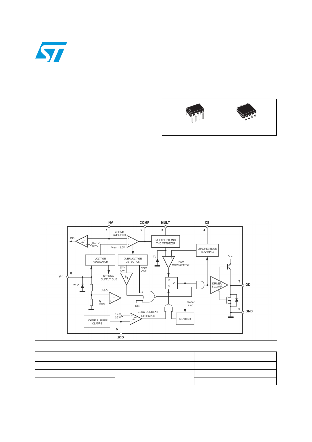
Figure 1. Block diagram
= 25 °C) internal reference voltage
J
L6562AT
Transition-mode PFC controller
SO-8DIP-8
■ DIP-8/SO-8 packages
Applications
PFC pre-regulators for:
■ Street lighting
■ IEC61000-3-2 compliant SMPS (Flat TV,
monitors, desktop PC, games)
■ Electronic ballast
Table 1. Device summary
Order codes Package Packaging
L6562ATN DIP-8 Tube
L6562ATD
L6562ATDTR Tape and reel
March 2009 Rev 2 1/25
SO-8
Tu be
www.st.com
25

Contents L6562AT
Contents
1 Description . . . . . . . . . . . . . . . . . . . . . . . . . . . . . . . . . . . . . . . . . . . . . . . . . 3
2 Pin settings . . . . . . . . . . . . . . . . . . . . . . . . . . . . . . . . . . . . . . . . . . . . . . . . 4
2.1 Pin connection . . . . . . . . . . . . . . . . . . . . . . . . . . . . . . . . . . . . . . . . . . . . . . 4
2.2 Pin description . . . . . . . . . . . . . . . . . . . . . . . . . . . . . . . . . . . . . . . . . . . . . . 4
3 Maximum ratings . . . . . . . . . . . . . . . . . . . . . . . . . . . . . . . . . . . . . . . . . . . . 5
4 Thermal data . . . . . . . . . . . . . . . . . . . . . . . . . . . . . . . . . . . . . . . . . . . . . . . 5
5 Electrical characteristics . . . . . . . . . . . . . . . . . . . . . . . . . . . . . . . . . . . . . 6
6 Typical electrical characteristic . . . . . . . . . . . . . . . . . . . . . . . . . . . . . . . . 8
7 Application information . . . . . . . . . . . . . . . . . . . . . . . . . . . . . . . . . . . . . 12
7.1 Overvoltage protection . . . . . . . . . . . . . . . . . . . . . . . . . . . . . . . . . . . . . . . 12
7.2 Disable function . . . . . . . . . . . . . . . . . . . . . . . . . . . . . . . . . . . . . . . . . . . . 13
7.3 THD optimizer circuit . . . . . . . . . . . . . . . . . . . . . . . . . . . . . . . . . . . . . . . . 13
7.4 Operating with no auxiliary winding on the boost inductor . . . . . . . . . . . . 15
7.5 Comparison between the L6562AT and the L6562 . . . . . . . . . . . . . . . . . 16
8 Application examples and ideas . . . . . . . . . . . . . . . . . . . . . . . . . . . . . . 17
9 Package mechanical data . . . . . . . . . . . . . . . . . . . . . . . . . . . . . . . . . . . . 21
10 Revision history . . . . . . . . . . . . . . . . . . . . . . . . . . . . . . . . . . . . . . . . . . . 24
2/25

Description L6562AT
1 Description
The L6562AT is a current-mode PFC controller operating in transition mode (TM). Coming
with the same pin-out as its predecessors L6561 and L6562, it offers improved performance.
The highly linear multiplier includes a special circuit, able to reduce AC input current
distortion, that allows wide-range-mains operation with an extremely low THD, even over a
large load range.
The output voltage is controlled by means of a voltage-mode error amplifier and an accurate
(1% @T
The device features extremely low consumption (60 µA max. before start-up and < 5.5 mA
operating) and includes a disable function suitable for IC remote ON/OFF, which makes it
easier to comply with energy saving requirements (Blue Angel, EnergyStar, Energy2000,
etc.).
An effective two-step OVP enables to safely handle over-voltages either occurring at startup or resulting from load disconnection.
The totem-pole output stage, capable of 600 mA source and 800 mA sink current, is suitable
to drive high current MOSFETs or IGBTs. This, combined with the other features and the
possibility to operate with the proprietary fixed-off-time control, makes the device an
excellent low-cost solution for EN61000-3-2 compliant SMPS in excess of 350 W.
= 25 °C) internal voltage reference.
J
3/25
Pin settings L6562AT
2 Pin settings
2.1 Pin connection
Figure 2. Pin connection (top view)
2.2 Pin description
Table 2. Pin description
Pin N° Name Description
Inverting input of the error amplifier. The information on the output voltage of
1INV
2COMP
3MULT
4CS
5ZCD
the PFC pre-regulator is fed into this pin through a resistor divider. The pin
doubles as an ON/OFF control input.
Output of the error amplifier. A compensation network is placed between this
pin and INV to achieve stability of the voltage control loop and ensure high
power factor and low THD.
Main input to the multiplier. This pin is connected to the rectified mains
voltage via a resistor divider and provides the sinusoidal reference to the
current loop.
Input to the PWM comparator. The current flowing in the MOSFET is sensed
through a resistor, the resulting voltage is applied to this pin and compared
with an internal sinusoidal-shaped reference, generated by the multiplier, to
determine MOSFET’s turn-off. The pin is equipped with 200 ns leading-edge
blanking for improved noise immunity.
Boost inductor’s demagnetization sensing input for transition-mode
operation. A negative-going edge triggers MOSFET’s turn-on.
INV
COMP
MULT
CS
1
2
3
4
Vcc
8
GD
7
GND
6
ZCD
5
6 GND Ground. Current return for both the signal part of the IC and the gate driver.
Gate driver output. The totem pole output stage is able to drive power
7GD
8Vcc
4/25
MOSFET’s and IGBT’s with a peak current of 600 mA source and 800 mA
sink. The high-level voltage of this pin is clamped at about 12 V to avoid
excessive gate voltages in case the pin is supplied with a high Vcc.
Supply voltage of both the signal part of the IC and the gate driver. The
supply voltage upper limit is extended to 22 V min. to provide more
headroom for supply voltage changes.
Maximum ratings L6562AT
3 Maximum ratings
Table 3. Absolute maximum ratings
Symbol Pin Parameter Value Unit
V
CC
I
GD
--- 1 to 4 Analog inputs and outputs -0.3 to 8 V
I
ZCD
8 IC supply voltage (ICC ≤ 20 mA) Self-limited V
7 Output totem pole peak current Self-limited A
5 Zero current detector max. current ±10 mA
4 Thermal data
Table 4. Thermal data
Symbol Parameter
R
P
T
thJA
TOT
T
STG
Max. thermal resistance, junction-toambient
Power dissipation @TA = 50 °C 0.65 1 W
Junction temperature operating range -40 to 150 °C
J
Storage temperature -55 to 150 °C
Val ue
Unit
SO8 DIP8
150 100 °C/W
5/25

Electrical characteristics L6562AT
5 Electrical characteristics
-40 °C < TJ < +125 °C, VCC = 12 V, CO = 1 nF; unless otherwise specified
Table 5. Electrical characteristics
Symbol Parameter Test condition Min Typ Max Unit
Supply voltage
V
Vcc
Vcc
CC
Operating range After turn-on 10.5 22.5 V
Turn-on threshold
On
Turn-off threshold
Off
(1)
(1)
11.7 12.5 13.3 V
9.5 10 10.5 V
Hys Hysteresis 2.2 2.8 V
V
Zener voltage ICC = 20 mA 22.5 25 28 V
Z
Supply current
I
start-up
I
I
CC
I
Start-up current Before turn-on, VCC = 11 V 30 60 µA
Quiescent current After turn-on 2.5 3.9 mA
q
Operating supply current @ 70 kHz 3.5 5.5 mA
Quiescent current
q
During OVP (either static or dynamic)
≤ 150 mV
or V
INV
1.7 2.2 mA
Multiplier input
I
MULT
V
MULT
VcsΔ
---------------------
V
Δ
MULT
K Gain
Input bias current V
= 0 to 4 V -1 µA
MULT
Linear operation range 0 to 3 V
= 0 to 1 V,
V
Output max. slope
(2)
MULT
V
COMP
V
MULT
= 1 V, V
= Upper clamp
COMP
11.1 V/V
= 4 V, 0.32 0.38 0.47 V
Error amplifier
= 25 °C 2.475 2.5 2.525
T
V
I
INV
INV
Voltage feedback input
threshold
Line regulation V
Input bias current V
J
10.5 V < V
= 10.5 V to 22.5 V 2 5 mV
CC
= 0 to 3 V -1 µA
INV
< 22.5 V
CC
(1)
2.44 2.545
Gv Voltage gain Open loop 60 80 dB
GB Gain-bandwidth product 1 MHz
I
COMP
V
COMP
V
INVdis
V
INVen
Source current V
Sink current V
Upper clamp voltage I
Lower clamp voltage I
Disable threshold 150 200 250 mV
Restart threshold 380 450 520 mV
COMP
COMP
SOURCE
= 0.5 mA
SINK
= 4 V, V
= 4 V, V
= 2.4 V -2 -3.5 -5 mA
INV
= 2.6 V 2.5 4.5 mA
INV
= 0.5 mA 5.1 5.7 6 V
(1)
2.12.252.4 V
6/25
V

Electrical characteristics L6562AT
(
−
⋅
Table 5. Electrical characteristics (continued)
Symbol Parameter Test condition Min Typ Max Unit
Output overvoltage
I
OVP
Dynamic OVP triggering
current
Hys Hysteresis
Static OVP threshold
Current sense comparator
td
Vcs
I
t
V
LEB
CS
(H-L)
CS
Input bias current VCS = 0 -1 µA
Leading edge blanking 100 200 300 ns
Delay to output 175 ns
Current sense clamp V
Current sense offset
offset
Zero current detector
V
V
V
V
ZCDH
ZCDL
ZCDA
ZCDT
Upper clamp voltage I
Lower clamp voltage I
Arming voltage
(positive-going edge)
Triggering voltage
(negative-going edge)
19.5 27 30.5 µA
(3)
(1)
= Upper clamp, Vmult = 1.5 V 1.0 1.08 1.16 V
COMP
V
= 0 25
MULT
= 2.5 V 5
V
MULT
= 2.5 mA 5.0 5.7 6.5 V
ZCD
= - 2.5 mA -0.5 0 0.5 V
ZCD
(3)
(3)
2.12.252.4 V
20 µA
1.4 V
0.7 V
mV
I
ZCDb
I
ZCDsrc
I
ZCDsnk
Input bias current V
= 1 to 4.5 V 2 µA
ZCD
Source current capability -1.5 mA
Sink current capability 1.5 mA
Starter
t
START
Start timer period 75 190 300 µs
Gate driver
V
OL
V
OH
I
srcpk
I
snkpk
t
t
V
Oclamp
1. All the parameters are in tracking
2. The multiplier output is given by:
3. Parameters guaranteed by design, functionality tested in production.
Output low voltage I
Output high voltage I
= 100 mA 0.6 1.2 V
sink
= 5 mA 9.5 10.3 V
source
Peak source current -0.6 A
Peak sink current 0.8 A
Voltage fall time 30 70 ns
f
Voltage rise time 60 130 ns
r
Output clamp voltage I
UVLO saturation Vcc = 0 to V
= ⋅
= 5 mA; Vcc = 20 V 10 12 15 V
source
, I
CCon
sink
COMPMULTcs
= 2 mA 1.1 V
)
5.2VVK V
7/25
Typical electrical characteristic L6562AT
pj
pj
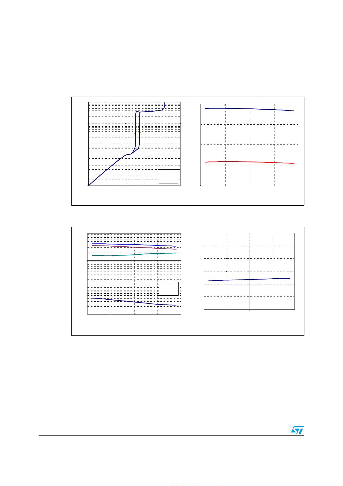
6 Typical electrical characteristic
Figure 3. Supply current vs supply
10.00
1.00
0.10
Icc (mA)
0.01
0.00
0.00 5. 00 10. 00 15.00 20.00 25.00
Figure 5. IC consumption vs T
10
1
voltage
Vcc (V)
Co = 1 nF
f = 70 kHz
Tj = 25°C
J
Ope rat ing
Quiescent
Disabled or during OVP
Figure 4. Start-up and UVLO vs TJ
13
Vcc-ON
12
11
(V)
10
Vcc-OFF
9
-50 0 50 100 150
Figure 6. Vcc Zener voltage vs T
28
27
26
Tj (°C)
J
Icc (mA)
0.01
0.1
-50 0 50 100 150
Tj (°C)
Vcc = 12 V
Co= 1 nF
f = 70 kHz
Before start-up
8/25
25
VccZ (V)
24
23
22
-50 0 50 100 150
Tj (°C)
 Loading...