

ST L6562A User Manual
现货库存、技术资料、百科信息、热点资讯,精彩尽在鼎好!
Features
■ Proprietary multiplier design for minimum thd
■ Very accurate adjustable output overvoltage
protection
■ Ultra-low (30µA) Start-up current
■ Low (2.5mA) quiescent current
■ Digital leading-edge blanking on current sense
■ Disable function on E/A input
■ 1.4% (@ T
■ -600/+800mA totem pole gate driver with active
pull-down during UVLO and voltage clamp
■ DIP-8/SO-8 packages
= 25 °C) internal reference voltage
J
L6562A
Transition-mode PFC controller
Preliminary Data
SO-8DIP-8
Applications
PFC pre-regulators for:
■ IEC61000-3-2 compliant SMPS (Flat TV,
desktop PC, games)
■ HI-END AC-DC adapter/charger up to 400W
■ Electronic ballast
■ Entry level server & web server
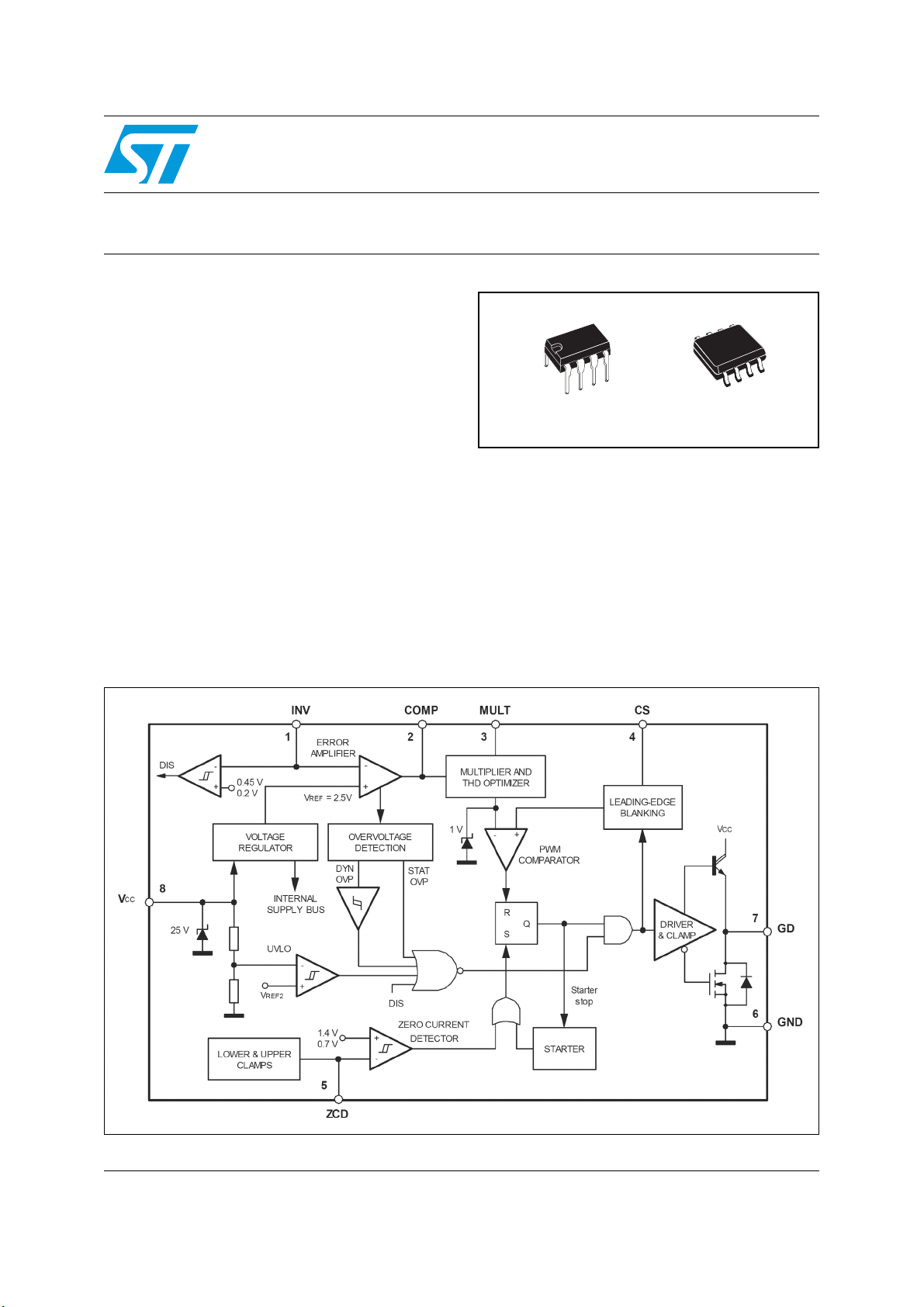
Figure 1. Block diagram
March 2007 Rev 1 1/20
This is preliminary information on a new product now in development or undergoing evaluation. Details are subject to
change without notice.
www.st.com
20

Contents L6562A
Contents
1 Description . . . . . . . . . . . . . . . . . . . . . . . . . . . . . . . . . . . . . . . . . . . . . . . . . 3
2 Pin settings . . . . . . . . . . . . . . . . . . . . . . . . . . . . . . . . . . . . . . . . . . . . . . . . 4
2.1 Pin connection . . . . . . . . . . . . . . . . . . . . . . . . . . . . . . . . . . . . . . . . . . . . . . 4
2.2 Pin description . . . . . . . . . . . . . . . . . . . . . . . . . . . . . . . . . . . . . . . . . . . . . . 4
3 Maximum ratings . . . . . . . . . . . . . . . . . . . . . . . . . . . . . . . . . . . . . . . . . . . . 5
4 Thermal data . . . . . . . . . . . . . . . . . . . . . . . . . . . . . . . . . . . . . . . . . . . . . . . 5
5 Electrical characteristics . . . . . . . . . . . . . . . . . . . . . . . . . . . . . . . . . . . . . 6
6 Application information . . . . . . . . . . . . . . . . . . . . . . . . . . . . . . . . . . . . . . 9
6.1 Overvoltage protection . . . . . . . . . . . . . . . . . . . . . . . . . . . . . . . . . . . . . . . . 9
6.2 Disable function . . . . . . . . . . . . . . . . . . . . . . . . . . . . . . . . . . . . . . . . . . . . 10
6.3 THD optimizer circuit . . . . . . . . . . . . . . . . . . . . . . . . . . . . . . . . . . . . . . . . 10
6.4 Operating with no auxiliary winding on the boost inductor . . . . . . . . . . . . 12
6.5 Comparison between the L6562A and the L6562 . . . . . . . . . . . . . . . . . . 13
7 Application examples and ideas . . . . . . . . . . . . . . . . . . . . . . . . . . . . . . 14
8 Package mechanical data . . . . . . . . . . . . . . . . . . . . . . . . . . . . . . . . . . . . 15
9 Order codes . . . . . . . . . . . . . . . . . . . . . . . . . . . . . . . . . . . . . . . . . . . . . . . 18
10 Revision history . . . . . . . . . . . . . . . . . . . . . . . . . . . . . . . . . . . . . . . . . . . 19
2/20

L6562A Description
1 Description
The L6562A is a current-mode PFC controller operating in Transition Mode (TM). Coming
with the same pin-out as its predecessors L6561 and L6562, it offers improved performance.
The highly linear multiplier includes a special circuit, able to reduce AC input current
distortion, that allows wide-range-mains operation with an extremely low THD, even over a
large load range.
The output voltage is controlled by means of a voltage-mode error amplifier and an accurate
(1.4% @T
The device features extremely low consumption (60µA max. before start-up and <5 mA
operating) and includes a disable function suitable for IC remote ON/OFF, which makes it
easier to comply with energy saving requirements (Blue Angel, EnergyStar, Energy2000,
etc.).
An effective two-step OVP enables to safely handle overvoltages either occurring at start-up
or resulting from load disconnection.
The totem-pole output stage, capable of 600 mA source and 800 mA sink current, is suitable
to drive high current MOSFETs or IGBTs. This, combined with the other features and the
possibility to operate with the proprietary Fixed-Off-Time control, makes the device an
excellent low-cost solution for EN61000-3-2 compliant SMPS in excess of 350W.
= 25°C) internal voltage reference.
J
3/20
Pin settings L6562A
2 Pin settings
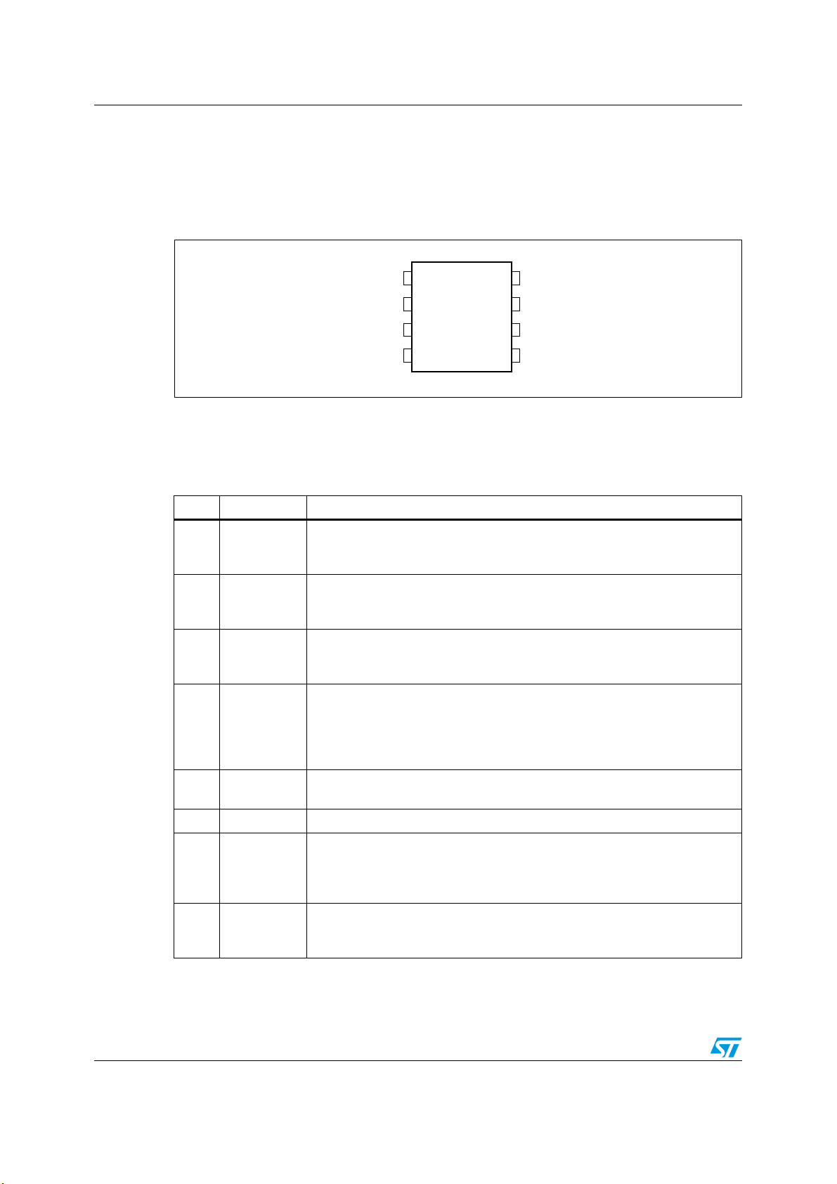
2.1 Pin connection
Figure 2. Pin connection (top view)
2.2 Pin description
Table 1. Pin description
Pin N° Name Description
Inverting input of the error amplifier. The information on the output voltage of
1INV
2COMP
3MULT
the PFC pre-regulator is fed into this pin through a resistor divider. The pin
doubles as an ON/OFF control input.
Output of the error amplifier. A compensation network is placed between this
pin and INV to achieve stability of the voltage control loop and ensure high
power factor and low THD.
Main input to the multiplier. This pin is connected to the rectified mains
voltage via a resistor divider and provides the sinusoidal reference to the
current loop.
INV
COMP
MULT
CS
1
2
3
4
Vcc
8
GD
7
GND
6
ZCD
5
Input to the PWM comparator. The current flowing in the MOSFET is sensed
through a resistor, the resulting voltage is applied to this pin and compared
4CS
5ZCD
6 GND Ground. Current return for both the signal part of the IC and the gate driver.
7GD
8Vcc
4/20
with an internal sinusoidal-shaped reference, generated by the multiplier, to
determine MOSFET’s turn-off. The pin is equipped with 200 ns leading-edge
blanking for improved noise immunity.
Boost inductor’s demagnetization sensing input for transition-mode
operation. A negative-going edge triggers MOSFET’s turn-on.
Gate driver output. The totem pole output stage is able to drive power
MOSFET’s and IGBT’s with a peak current of 600 mA source and 800 mA
sink. The high-level voltage of this pin is clamped at about 12V to avoid
excessive gate voltages in case the pin is supplied with a high Vcc.
Supply Voltage of both the signal part of the IC and the gate driver. The
supply voltage upper limit is extended to 22V min. to provide more headroom
for supply voltage changes.

L6562A Maximum ratings
3 Maximum ratings
Table 2. Absolute maximum ratings
Symbol Pin Parameter Value Unit
V
CC
I
GD
--- 1 to 4 Analog inputs & outputs -0.3 to 8 V
I
ZCD
8 IC supply voltage (ICC ≤ 20mA) Self-limited V
7 Output totem pole peak current Self-limited A
5 Zero current detector max. current ±10 mA
4 Thermal data
Table 3. Thermal data
Symbol Parameter
SO8 DIP8
Val ue
Unit
R
P
T
thJA
TOT
T
J
STG
Max. Thermal Resistance, Junction-toambient
Power Dissipation @TA = 50°C 0.65 1 W
Junction Temperature Operating range -40 to 150 °C
Storage Temperature -55 to 150 °C
150 100 °C/W
5/20

Electrical characteristics L6562A
5 Electrical characteristics
Table 4. Electrical characteristics
( -25°C < T
Symbol Parameter Test condition Min Typ Max Unit
Supply voltage
< +125°C, VCC = 12V, Co = 1nF; unless otherwise specified)
J
V
Vcc
Vcc
CC
Operating range After turn-on 10.5 22 V
Turn-on threshold 11.5 12.5 13.5 V
On
Turn-off threshold
Off
(1)
9.5 10 10.5 V
Hys Hysteresis 2.2 2.8 V
V
Z
Zener Voltage
= 20mA
I
CC
22 25 28 V
Supply current
I
start-up
I
q
I
CC
I
q
Start-up current
Quiescent current After turn-on 2.5 3.75 mA
Operating supply current @ 70kHz 3.5 5 mA
Quiescent current
Before turn-on, V
CC
= 11V
During OVP (either static or dynamic)
or V
≤150mV
INV
30 60 µA
1.7 2.2 mA
Multiplier input
I
MULT
V
MULT
Vcs∆
---------------------
V
∆
MULT
K
Input bias current
Linear operation range 0 to 3 V
Output max. slope
(2)
Gain
V
MULT
V
MULT
V
COMP
V
MULT
= 1V, V
= 0 to 4V
= 0 to 1V,
= Upper clamp
= 4V,
COMP
-1 µA
11.1 V/V
0.32 0.38 0.44 V
Error amplifier
= 25 °C
V
I
INV
INV
Voltage feedback input
threshold
Line regulation
Input bias current
T
J
10.5V < V
= 10.5V to 22V
V
CC
= 0 to 3V
V
INV
CC
< 22V
(1)
2.465 2.5 2.535
2.44 2.56
25mV
-1 µA
Gv Voltage gain Open loop 60 80 dB
GB Gain-bandwidth product 1 MHz
I
COMP
Source current
Sink current
V
COMP
V
COMP
= 4V, V
= 4V, V
INV
INV
= 2.4V
= 2.6V
-2 -3.5 -5 mA
2.5 4.5 mA
6/20
V
 Loading...