

Features
■ Proprietary multiplier design for minimum THD
■ Very accurate adjustable output overvoltage
protection
■ Ultra-low (30µA) Start-up current
■ Low (2.5mA) quiescent current
■ Digital leading-edge blanking on current sense
■ Disable function on E/A input
■ 1% (@ T
■ -600/+800mA totem pole gate driver with active
pull-down during UVLO and voltage clamp
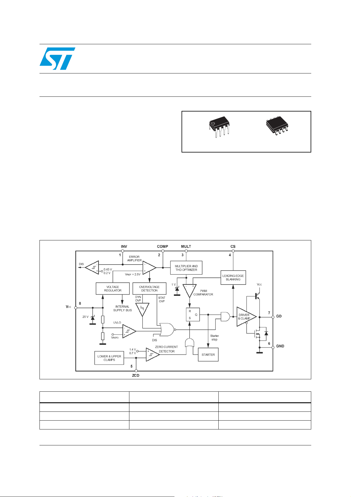
■ DIP-8/SO-8 packages
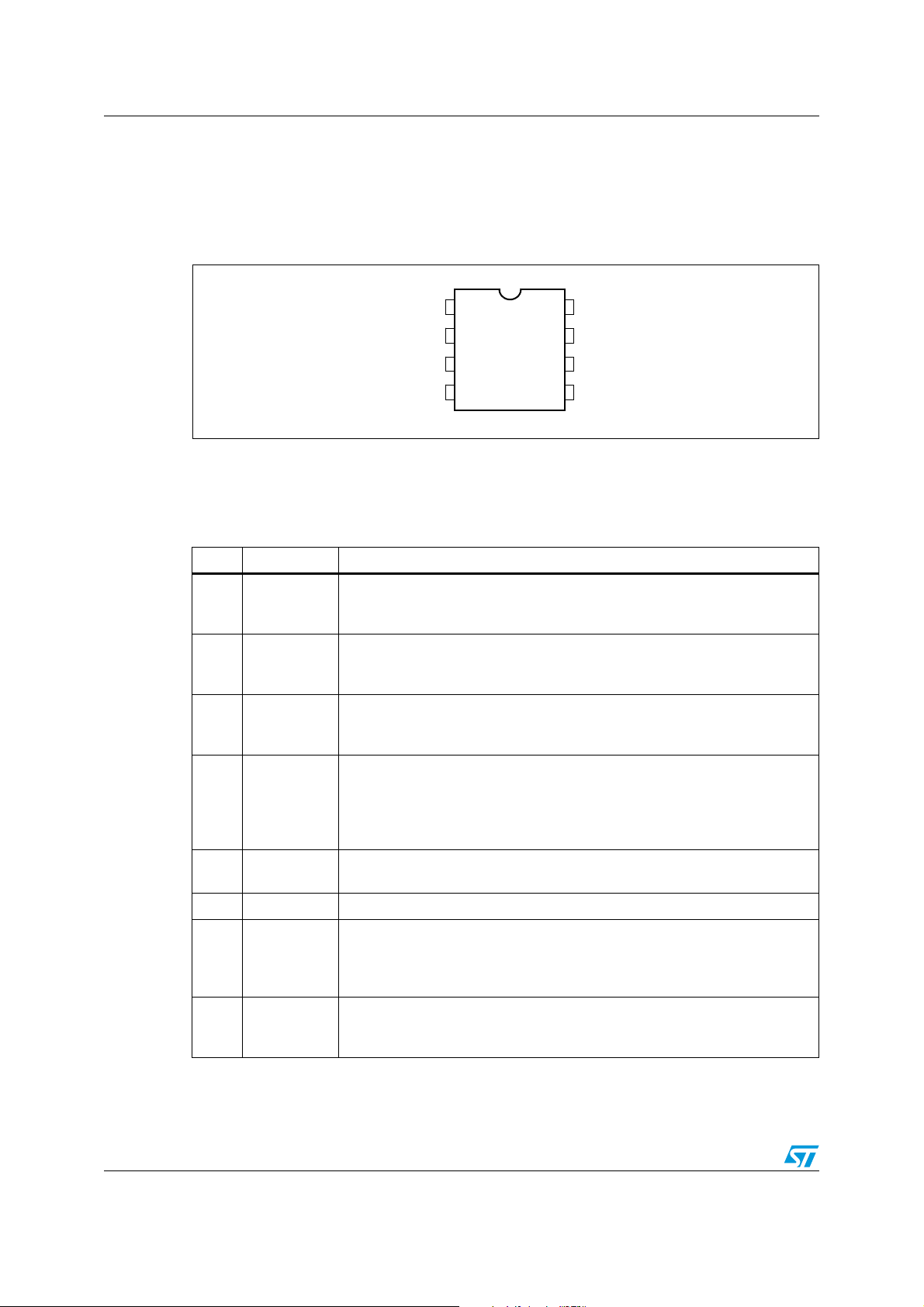
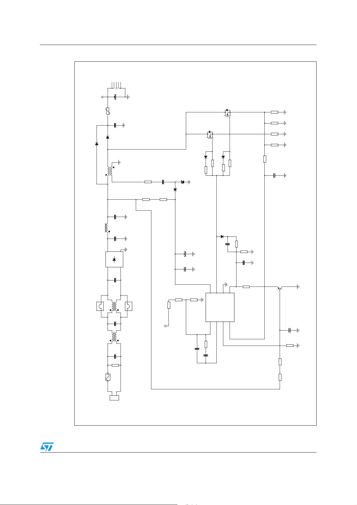
Figure 1. Block diagram
= 25 °C) internal reference voltage
J
L6562A
Transition-mode PFC controller
SO-8DIP-8
Applications
PFC pre-regulators for:
■ IEC61000-3-2 compliant SMPS (Flat TV,
monitors, desktop PC, games)
■ HI-END AC-DC adapter/charger up to 400W
■ Electronic ballast
■ Entry level server & web server
Table 1. Device summary
Order codes Package Packaging
L6562AN DIP-8 Tube
L6562AD SO-8 Tube
L6562ADTR SO-8 Tape & Reel
August 2007 Rev 3 1/26
www.st.com
26

Contents L6562A
Contents
1 Description . . . . . . . . . . . . . . . . . . . . . . . . . . . . . . . . . . . . . . . . . . . . . . . . . 3
2 Pin settings . . . . . . . . . . . . . . . . . . . . . . . . . . . . . . . . . . . . . . . . . . . . . . . . 4
2.1 Pin connection . . . . . . . . . . . . . . . . . . . . . . . . . . . . . . . . . . . . . . . . . . . . . . 4
2.2 Pin description . . . . . . . . . . . . . . . . . . . . . . . . . . . . . . . . . . . . . . . . . . . . . . 4
3 Maximum ratings . . . . . . . . . . . . . . . . . . . . . . . . . . . . . . . . . . . . . . . . . . . . 5
4 Thermal data . . . . . . . . . . . . . . . . . . . . . . . . . . . . . . . . . . . . . . . . . . . . . . . 5
5 Electrical characteristics . . . . . . . . . . . . . . . . . . . . . . . . . . . . . . . . . . . . . 6
6 Typical electrical characteristic . . . . . . . . . . . . . . . . . . . . . . . . . . . . . . . . 9
7 Application information . . . . . . . . . . . . . . . . . . . . . . . . . . . . . . . . . . . . . 13
7.1 Overvoltage protection . . . . . . . . . . . . . . . . . . . . . . . . . . . . . . . . . . . . . . . 13
7.2 Disable function . . . . . . . . . . . . . . . . . . . . . . . . . . . . . . . . . . . . . . . . . . . . 14
7.3 THD optimizer circuit . . . . . . . . . . . . . . . . . . . . . . . . . . . . . . . . . . . . . . . . 14
7.4 Operating with no auxiliary winding on the boost inductor . . . . . . . . . . . . 16
7.5 Comparison between the L6562A and the L6562 . . . . . . . . . . . . . . . . . . 17
8 Application examples and ideas . . . . . . . . . . . . . . . . . . . . . . . . . . . . . . 18
9 Package mechanical data . . . . . . . . . . . . . . . . . . . . . . . . . . . . . . . . . . . . 22
10 Revision history . . . . . . . . . . . . . . . . . . . . . . . . . . . . . . . . . . . . . . . . . . . 25
2/26

L6562A Description
1 Description
The L6562A is a current-mode PFC controller operating in Transition Mode (TM). Coming
with the same pin-out as its predecessors L6561 and L6562, it offers improved performance.
The highly linear multiplier includes a special circuit, able to reduce AC input current
distortion, that allows wide-range-mains operation with an extremely low THD, even over a
large load range.
The output voltage is controlled by means of a voltage-mode error amplifier and an accurate
(1% @T
The device features extremely low consumption (60µA max. before start-up and <5 mA
operating) and includes a disable function suitable for IC remote ON/OFF, which makes it
easier to comply with energy saving requirements (Blue Angel, EnergyStar, Energy2000,
etc.).
An effective two-step OVP enables to safely handle overvoltages either occurring at start-up
or resulting from load disconnection.
The totem-pole output stage, capable of 600 mA source and 800 mA sink current, is suitable
to drive high current MOSFETs or IGBTs. This, combined with the other features and the
possibility to operate with the proprietary Fixed-Off-Time control, makes the device an
excellent low-cost solution for EN61000-3-2 compliant SMPS in excess of 350W.
= 25°C) internal voltage reference.
J
3/26
Pin settings L6562A
2 Pin settings
2.1 Pin connection
Figure 2. Pin connection (top view)
2.2 Pin description
Table 2. Pin description
Pin N° Name Description
Inverting input of the error amplifier. The information on the output voltage of
1INV
2COMP
3MULT
the PFC pre-regulator is fed into this pin through a resistor divider. The pin
doubles as an ON/OFF control input.
Output of the error amplifier. A compensation network is placed between this
pin and INV to achieve stability of the voltage control loop and ensure high
power factor and low THD.
Main input to the multiplier. This pin is connected to the rectified mains
voltage via a resistor divider and provides the sinusoidal reference to the
current loop.
INV
COMP
MULT
CS
1
2
3
4
Vcc
8
GD
7
GND
6
ZCD
5
Input to the PWM comparator. The current flowing in the MOSFET is sensed
through a resistor, the resulting voltage is applied to this pin and compared
4CS
5ZCD
6 GND Ground. Current return for both the signal part of the IC and the gate driver.
7GD
8Vcc
4/26
with an internal sinusoidal-shaped reference, generated by the multiplier, to
determine MOSFET’s turn-off. The pin is equipped with 200 ns leading-edge
blanking for improved noise immunity.
Boost inductor’s demagnetization sensing input for transition-mode
operation. A negative-going edge triggers MOSFET’s turn-on.
Gate driver output. The totem pole output stage is able to drive power
MOSFET’s and IGBT’s with a peak current of 600 mA source and 800 mA
sink. The high-level voltage of this pin is clamped at about 12V to avoid
excessive gate voltages in case the pin is supplied with a high Vcc.
Supply Voltage of both the signal part of the IC and the gate driver. The
supply voltage upper limit is extended to 22V min. to provide more headroom
for supply voltage changes.
L6562A Maximum ratings
3 Maximum ratings
Table 3. Absolute maximum ratings
Symbol Pin Parameter Value Unit
V
CC
I
GD
--- 1 to 4 Analog inputs & outputs -0.3 to 8 V
I
ZCD
8 IC supply voltage (ICC ≤ 20mA) Self-limited V
7 Output totem pole peak current Self-limited A
5 Zero current detector max. current ±10 mA
4 Thermal data
Table 4. Thermal data
Symbol Parameter
SO8 DIP8
Val ue
Unit
R
P
T
thJA
TOT
T
J
STG
Max. Thermal Resistance, Junction-toambient
Power Dissipation @TA = 50°C 0.65 1 W
Junction Temperature Operating range -40 to 150 °C
Storage Temperature -55 to 150 °C
150 100 °C/W
5/26
Electrical characteristics L6562A
5 Electrical characteristics
Table 5. Electrical characteristics
( -25°C < T
Symbol Parameter Test condition Min Typ Max Unit
Supply voltage
< +125°C, VCC = 12V, Co = 1nF; unless otherwise specified)
J
V
Vcc
Vcc
CC
Operating range After turn-on 10.5 22.5 V
Turn-on threshold
On
Turn-off threshold
Off
(1)
(1)
11.7 12.5 13.3 V
9.5 10 10.5 V
Hys Hysteresis 2.2 2.8 V
V
Z
Zener Voltage
= 20mA
I
CC
22.5 25 28 V
Supply current
I
start-up
I
q
I
CC
I
q
Start-up current
Quiescent current After turn-on 2.5 3.75 mA
Operating supply current @ 70kHz 3.5 5 mA
Quiescent current
Before turn-on, V
CC
= 11V
During OVP (either static or dynamic)
or V
≤150mV
INV
30 60 µA
1.7 2.2 mA
Multiplier input
I
MULT
V
MULT
Vcs∆
---------------------
V
∆
MULT
K
Input bias current
Linear operation range 0 to 3 V
Output max. slope
(2)
Gain
V
MULT
V
MULT
V
COMP
V
MULT
= 1V, V
= 0 to 4V
= 0 to 1V,
= Upper clamp
= 4V,
COMP
-1 µA
11.1 V/V
0.32 0.38 0.44 V
Error amplifier
= 25 °C
V
I
INV
INV
Voltage feedback input
threshold
Line regulation
Input bias current
T
J
10.5V < V
V
CC
V
INV
CC
= 10.5V to 22.5V
= 0 to 3V
< 22.5V
(1)
2.475 2.5 2.525
2.455 2.545
25mV
-1 µA
Gv Voltage gain Open loop 60 80 dB
GB Gain-bandwidth product 1 MHz
I
COMP
Source current
Sink current
V
COMP
V
COMP
= 4V, V
= 4V, V
INV
INV
= 2.4V
= 2.6V
-2 -3.5 -5 mA
2.5 4.5 mA
6/26
V

L6562A Electrical characteristics
Table 5. Electrical characteristics (continued)
( -25°C < T
Symbol Parameter Test condition Min Typ Max Unit
< +125°C, VCC = 12V, Co = 1nF; unless otherwise specified)
J
V
COMP
V
INVdis
V
INVen
Lower clamp voltage
Disable threshold 150 200 250 mV
Restart threshold 380 450 520 mV
Output overvoltage
Upper clamp voltage
I
OVP
Dynamic OVP triggering
current
Hys Hysteresis
Static OVP threshold
Current sense comparator
td
Vcs
I
t
V
LEB
CS
(H-L)
CS
Input bias current
Leading edge blanking 100 200 300 ns
Delay to output 175 ns
Current sense clamp
Current sense offset
offset
I
SOURCE
I
SINK
(3)
(1)
V
V
V
V
= 0.5mA
= 0.5mA
= 0
CS
COMP
MULT
MULT
= 0
= 2.5V
(1)
= Upper clamp, Vmult = 1.5V
5.3 5.7 6 V
2.12.252.4 V
23.5 27 30.5 µA
20 µA
2.12.252.4 V
-1 µA
1.0 1.08 1.16 V
25
mV
5
Zero current detector
V
ZCDH
V
ZCDL
V
ZCDA
V
ZCDT
I
ZCDb
I
ZCDsrc
I
ZCDsnk
Upper clamp voltage
Lower clamp voltage
Arming voltage
(positive-going edge)
Triggering voltage
(negative-going edge)
Input bias current
Source current capability -2.5 mA
Sink current capability 2.5 mA
Starter
t
START
Start timer period 75 190 300 µs
I
ZCD
I
ZCD
(3)
(3)
V
ZCD
= 2.5mA
= - 2.5mA
= 1 to 4.5V
5.0 5.7 6.5 V
-0.3 0 0.3 V
1.4 V
0.7 V
2µA
7/26
Electrical characteristics L6562A
(
−
⋅
Table 5. Electrical characteristics (continued)
( -25°C < T
Symbol Parameter Test condition Min Typ Max Unit
Gate driver
< +125°C, VCC = 12V, Co = 1nF; unless otherwise specified)
J
V
OL
V
OH
I
srcpk
I
snkpk
t
t
V
Oclamp
1. All the parameters are in tracking
2. The multiplier output is given by:
3. Parameters guaranteed by design, functionality tested in production.
Output low voltage I
Output high voltage I
= 100mA 0.6 1.2 V
sink
= 5mA 9.8 10.3 V
source
Peak source current -0.6 A
Peak sink current 0.8 A
Voltage fall time 30 70 ns
f
Voltage rise time 60 110 ns
r
Output clamp voltage I
UVLO saturation Vcc = 0 to V
= ⋅
= 5mA; Vcc = 20 V 10 12 15 V
source
, I
CCon
sink
COMPMULTcs
= 2 mA 1.1 V
)
5.2VVK V
8/26

L6562A Typical electrical characteristic
pj
pj
6 Typical electrical characteristic
Figure 3. Supply current vs supply
10.00
1.00
0.10
Icc (mA)
0.01
0.00
0.00 5. 00 10.00 15.00 20.00 25.00
Figure 5. IC consumption vs T
10
1
voltage
Vcc (V)
Co = 1 nF
f = 70 kHz
Tj = 25°C
J
Ope rat ing
Quiescent
Disabled or during OVP
Figure 4. Start-up & UVLO vs TJ
13
Vcc-ON
12
11
(V)
10
Vcc-OFF
9
-50 0 50 100 150
Tj (°C)
Figure 6. Vcc Zener voltage vs T
28
27
26
J
Icc (mA)
0.01
0.1
-50 0 50 1 00 150
Tj (°C)
Vcc = 12 V
Co= 1 nF
f = 70 kHz
Before start-up
25
VccZ (V)
24
23
22
-50 0 50 100 150
Tj (°C)
9/26

Typical electrical characteristic L6562A
j
Figure 7. Feedback reference vs T
2.6
2.55
2.5
VREF (V)
2.45
2.4
-50 0 50 100 150
Figure 9. E/A output clamp levels vs TJFigure 10. Delay-to-output vsT
6
5
4
3
V COMP pin2 (V)
2
Tj (°C)
J
Vcc = 12V
Uppe r cl am p
Vcc = 12V
Lower clam p
Figure 8. OVP current vs T
35
34
33
32
31
30
29
Iovp (uA)
28
27
26
25
24
23
-50 0 50 100 150
300
200
tD (H-L) (ns)
100
Tj (°C)
J
Vcc = 12V
J
Vcc = 12V
1
-50 0 50 100 150
Tj (°C)
10/26
0
-50 0 50 100 150
Tj (°C)

L6562A Typical electrical characteristic
p
V
pj
pj
Figure 11. Multiplier characteristic Figure 12. Vcs clamp vs T
1.2
Upper Volt. Clamp
1.1
1.0
0.9
0.8
0.7
0.6
0.5
Vcs (pi n4) (V)
0.4
0.3
0.2
0.1
0.0
-0.1
Figure 13. ZCD clamp levels vs T
7
6
5
4
3
Vzcd (V)
2
5.75 V
5 V
4.5V
0 0.2 0.4 0.6 0.8 1 1.2 1. 4 1.6 1.8 2 2.2 2. 4 2. 6 2.8 3
VMULT (pin3) (V)
V COMP (pin2) (V
4 V
J
Uppe r cl am p
Vcc = 12V
IZCD = ±2. 5 mA
3.5V
3 V
2.5
1.3
)
1.2
Vcsx (V)
1.1
1
-50 0 50 100 150
Tj (°C)
Figure 14. Start-up timer vs T
200
190
180
Tstart (us)
170
J
Vcc = 12V
VCOMP = Upper clamp
J
Vcc = 12V
1
0
-1
-50 0 50 100 150
Tj (°C)
Lower clam p
160
150
-50 0 50 100 150
Tj (°C)
11/26

Typical electrical characteristic L6562A
Figure 15. Gate-driver output low
5.00
4.00
3.00
Vpin7 (V)
2.00
1.00
0.00
0 200 400 600 800 1000
Figure 17. Gate-drive clamp vs T
13.5
13.25
13
Vpin 7 clamp (V)
12.75
saturation
I GD (mA)
Tj = 25 °C
Vcc = 12V
SINK
J
Vcc = 20V
Figure 16. Gate-drive output high
saturation
12.00
11.00
10.00
9.00
Vpin7 (V)
8.00
7.00
6.00
0 200 400 600
I GD (mA)
Figure 18. Output gate drive low
saturation vs T
1.1
1
Vcc = 11V
0.9
Vcc = 0V
0.8
Vpin7 (V)
0.7
0.6
during UVLO
J
Isink = 2 m A
Tj = 25 °C
Vcc = 12V
SOURCE
12.5
-50 0 50 100 150
Tj (°C)
12/26
0.5
-50 0 50 100 150
Tj (°C)

L6562A Application information
7 Application information
7.1 Overvoltage protection
Under steady-state conditions, the voltage control loop keeps the output voltage Vo of a
PFC pre-regulator close to its nominal value, set by the resistors R1 and R2 of the output
divider. Neglecting ripple components, the current through R1, I
I
. Considering that the non-inverting input of the error amplifier is internally referenced at
R2
2.5V, also the voltage at pin INV will be 2.5V, then:
Equation 1
V
I
R2IR1
2.5
------- -
R2
O
--------------------- -===
2.5–
R1
If the output voltage experiences an abrupt change ∆Vo > 0 due to a load drop, the voltage
at pin INV will be kept at 2.5V by the local feedback of the error amplifier, a network
connected between pins INV and COMP that introduces a long time constant to achieve
high PF (this is why ∆Vo can be large). As a result, the current through R2 will remain equal
to 2.5/R2 but that through R1 will become:
, equals that through R2,
R1
Equation 2
VO2.5– VO∆+
I'
--------------------------------------- -=
R1
R1
The difference current ∆IR1=I'R1-IR2=I'R1-IR1= ∆Vo/R1 will flow through the compensation
network and enter the error amplifier output (pin COMP). This current is monitored inside
the device and if it reaches about 24µA the output voltage of the multiplier is forced to
decrease, thus smoothly reducing the energy delivered to the output. As the current
exceeds 27µA, the OVP is triggered (Dynamic OVP): the gate-drive is forced low to switch
off the external power transistor and the IC put in an idle state. This condition is maintained
until the current falls below approximately 7µA, which re-enables the internal starter and
allows switching to restart. The output ∆Vo that is able to trigger the Dynamic OVP function
is then:
Equation 3
∆
VO = R1 · 20 · 10
- 6
An important advantage of this technique is that the OV level can be set independently of
the regulated output voltage: the latter depends on the ratio of R1 to R2, the former on the
individual value of R1. Another advantage is the precision: the tolerance of the detection
current is 13%, i.e. 13% tolerance on ∆Vo. Since ∆Vo << Vo, the tolerance on the absolute
value will be proportionally reduced.
Example: Vo = 400V, ∆Vo = 40V. Then: R1 = 40V/27µA
≈ 1.5MΩ ;
R2 = 1.5 MΩ ·2.5/(400-2.5) = 9.43kΩ. The tolerance on the OVP level due to the L6562A will
be 40·0.13 = 5.3V, that is ± 1.2%.
13/26

Application information L6562A
When the load of a PFC pre-regulator is very low, the output voltage tends to stay steadily
above the nominal value, which cannot be handled by the Dynamic OVP. If this occurs,
however, the error amplifier output will saturate low; hence, when this is detected the
external power transistor is switched off and the IC put in an idle state (Static OVP). Normal
operation is resumed as the error amplifier goes back into its linear region. As a result, the
device will work in burst-mode, with a repetition rate that can be very low.
When either OVP is activated the quiescent consumption of the IC is reduced to minimize
the discharge of the Vcc capacitor and increase the hold-up capability of the IC supply
system.
7.2 Disable function
The INV pin doubles its function as a not-latched IC disable: a voltage below 0.2V shuts
down the IC and reduces its consumption at a lower value. To restart the IC, the voltage on
the pin must exceed 0.45 V. The main usage of this function is a remote ON/OFF control
input that can be driven by a PWM controller for power management purposes. However it
also offers a certain degree of additional safety since it will cause the IC to shutdown in case
the lower resistor of the output divider is shorted to ground or if the upper resistor is missing
or fails open.
7.3 THD optimizer circuit
The device is equipped with a special circuit that reduces the conduction dead-angle
occurring to the AC input current near the zero-crossings of the line voltage (crossover
distortion). In this way the THD (Total Harmonic Distortion) of the current is considerably
reduced.
A major cause of this distortion is the inability of the system to transfer energy effectively
when the instantaneous line voltage is very low. This effect is magnified by the highfrequency filter capacitor placed after the bridge rectifier, which retains some residual
voltage that causes the diodes of the bridge rectifier to be reverse-biased and the input
current flow to temporarily stop.
14/26

L6562A Application information
Figure 19. THD optimization: standard TM PFC controller (left side) and L6562A
(right side)
Input current Input current
Rectified mains voltage Rectified mains voltage
Imains
Input current
MOSFET's drain voltage
Vdrain
Imains
Input current
MOSFET's drain voltage
Vdrain
To overcome this issue the circuit embedded in the device forces the PFC pre-regulator to
process more energy near the line voltage zero-crossings as compared to that commanded
by the control loop. This will result in both minimizing the time interval where energy transfer
is lacking and fully discharging the high-frequency filter capacitor after the bridge. The effect
of the circuit is shown in figure 2, where the key waveforms of a standard TM PFC controller
are compared to those of the L6562A.
Essentially, the circuit artificially increases the ON-time of the power switch with a positive
offset added to the output of the multiplier in the proximity of the line voltage zero-crossings.
This offset is reduced as the instantaneous line voltage increases, so that it becomes
negligible as the line voltage moves toward the top of the sinusoid.
To maximally benefit from the THD optimizer circuit, the high-frequency filter capacitor after
the bridge rectifier should be minimized, compatibly with EMI filtering needs. A large
capacitance, in fact, introduces a conduction dead-angle of the AC input current in itself even with an ideal energy transfer by the PFC pre-regulator - thus making the action of the
optimizer circuit little effective.
15/26

Application information L6562A
7.4 Operating with no auxiliary winding on the boost inductor
To generate the synchronization signal on the ZCD pin, the typical approach requires the
connection between the pin and an auxiliary winding of the boost inductor through a limiting
resistor. When the device is supplied by the cascaded DC-DC converter, it is necessary to
introduce a supplementary winding to the PFC choke just to operate the ZCD pin.
Another solution could be implemented by simply connecting the ZCD pin to the drain of the
power MOSFET through an R-C network as shown in figure 3: in this way the highfrequency edges experienced by the drain will be transferred to the ZCD pin, hence arming
and triggering the ZCD comparator.
Also in this case the resistance value must be properly chosen to limit the current
sourced/sunk by the ZCD pin. In typical applications with output voltages around 400V,
recommended values for these components are 22pF (or 33pF) for C
R
. With these values proper operation is guaranteed even with few volts difference
ZCD
between the regulated output voltage and the peak input voltage
Figure 20. ZCD pin synchronization without auxiliary winding
ZCD
C
ZCD
R
and 330k for
ZCD
ZCD
5
L6562A
16/26

L6562A Application information
7.5 Comparison between the L6562A and the L6562
The L6562A is not a direct drop-in replacement of the L6562, even if both have the same
pin-out. One function (Disable) has been relocated.
Table 2 compares the two devices, i.e. those parameters that may result in different values
of the external components. The parameters that have the most significant impact on the
design, i.e. that definitely require external component changes when converting an L6562based design to the L6562A, are highlighted in bold.
Table 6. L6562A vs. L6562
Parameter L6562 L6562A
IC turn-on & turn-off thresholds (typ.) 12/9.5 V 12.5/10 V
Turn-off threshold spread (max.) ±0.8 V ±0.5 V
IC consumption before start-up (max.) 70 uA 60 uA
Multiplier gain (typ.) 0.6 0.38
Current sense reference clamp (typ.) 1.7 V 1.08 V
Current sense propagation delay (delay-to-output) (typ.) 200 ns 175 ns
Dynamic OVP triggering current (typ.) 40 uA 27 uA
ZCD arm/trigger/clamp thresholds (typ.) 2.1/1.4/0.7 V 1.4/0.7/0 V
Enable threshold (typ.)
Gate-driver internal drop (max.) 2.6 V 2.2 V
Leading-edge blanking on current sense No Yes
Reference voltage accuracy ( overall) 2.4% 1.8%
1. Function located on pin 5 (ZCD)
2. Function located on pin 1 (INV)
0.3 V
(1)
0.45 V
(2)
The lower value (-36%) for the clamp level of the current sense reference voltage allows the
use of a lower sense resistor for the same peak current, with a proportional reduction of the
associated power dissipation. Essentially, the advantage is the reduction of the power
dissipated in a single point (hotspot), which is a considerable benefit in applications where
heat removal is critical, e.g. in adapters enclosed in a sealed plastic case. The lower value
for the Dynamic OVP triggering current allows the use of a higher resistance value (+48%)
for the upper resistor of the divider sensing the output voltage of the PFC stage (keeping the
same overvoltage level) with no significant increase of noise sensitivity. This reduction goes
in favor of standby consumption in applications required to comply with energy saving
regulations.
17/26

Application examples and ideas L6562A
8 Application examples and ideas
Figure 21. Demo board EVL6562A-TM-80W, wide-range mains : electrical schematic
Vo=400V
Vo=400V
Po=80W
Po=80W
R11
R11
Ω
Ω
1M
1M
R12
R12
1M
1M
Ω
Ω
C6
C6
47 µF
47 µF
450V
450V
R13B
R13B
82 k
82 k
Ω
Ω
Ω
Ω
F1
F1
4A/250V
4A/250V
Vac
Vac
88V
88V
to
to
264V
264V
R4
R4
Ω
Ω
270 k
270 k
270 k
270 k
R1
R1
1 M
1 M
Ω
Ω
C1
P1
P1
+
+
W08
W08
-
-
Boost Inductor Spec (ITACOIL E2543/E)
Boost Inductor Spec (ITACOIL E2543/E)
C1
0.22 µF
0.22 µF
630V
630V
R2
R2
1 M
1 M
Ω
Ω
C2
C2
10nF
10nF
R3
R3
15 k
15 k
Ω
Ω
E25x13x7 core, N67 ferrite
E25x13x7 core, N67 ferrite
1.5 mm gap for 0. 7 mH primary induct ance
1.5 mm gap for 0. 7 mH primary induct ance
Primary: 102 turns 20x0.1 mm
Primary: 102 turns 20x0.1 mm
Secondary: 10 turns 0.1 mm
Secondary: 10 turns 0.1 mm
R5
R5
C29
C29
22 µF
22 µF
25V
25V
Ω
Ω
D8
D8
1N4148
1N4148
D2
D2
1N5248B
1N5248B
C5
C5
10 nF
10 nF
VCC
VCC
MULT
MULT
100 nF
100 nF
R14
R14
100
100
Ω
Ω
R6
R6
47 k
47 k
Ω
Ω
ZCD COMP INV
ZCD COMP INV
8
8
3
3
GND
GND
C4
C4
T1
T1
C3 - 2200 nF
C3 - 2200 nF
5
21
5
21
L6562A
L6562A
6
6
C23
C23
150 nF
150 nF
CS
CS
R50 - 22 kΩ
R50 - 22 kΩ
GD
GD
7
7
4
4
R15
R15
SHORTED
SHORTED
R8
R8
47k
47k
D1
D1
NTC
STP8NM50FP
STP8NM50FP
R10
R10
0.68 Ω
0.68 Ω
0.25W
0.25W
NTC
2.5
2.5
Ω
Ω
Q1
Q1
R13
R13
15 k
15 k
STTH1L06
STTH1L06
R7
R7
33
33
Ω
Ω
Ω
Ω
R9
R9
0.68 Ω
0.68 Ω
0.25W
0.25W
18/26

L6562A Application examples and ideas
Figure 22. L6562A 80W TM PFC evaluation
Figure 23. L6562A 80W TM PFC evaluation
board: compliance to EN61000-3-2
0.0 1
0.001
Harmonic current (A)
0. 0001
Vin = 230 Vac - 50 Hz, Pout = 80 W
THD = 10.48 %, PF = 0.973
standard
Mea sur ements @ 230V ac Ful l load EN61000-3 -2 cl ass D li mit s
1
0. 1
1 3 5 7 9 11131517192123252729313335 37 39
Harmonic Order (n)
Vin = 100 Vac - 50 Hz, Pout = 80 W
THD = 3.18 %, PF = 0.997
Figure 24. Figure 3 - L6562A 80W TM PFC
Evaluation board: Input Current
waveform @230V-50Hz – 80W load
board: compliance to JEIDA-MITI
standard
Meas ure ment s @ 10 0Vac Full lo ad JEIDA-MITI class D limits
1
0. 1
0.0 1
0.001
Harm onic current (A)
0. 0001
1 3 5 7 9 1113151719 212325 272931 3335 37 39
Harmonic Order (n)
Figure 25. Figure 4- L6562A 80W TM PFC
Evaluation board: Input Current
waveform @100V-50Hz – 80W load
19/26

Application examples and ideas L6562A
)
Figure 26. L6562A 80W TM PFC evaluation
1.00
0.95
0.90
PF
0.85
0.80
80 100 120 140 160 180 200 220 240 26 0
board: Power Factor vs Vin
Pout = 80W
Vin (Vac)
Figure 28. L6562A 80W TM PFC evaluation
board: efficiency vs Vin
100
95
90
85
EFFICIENCY (%)
80
75
80 100 120 140 160 180 200 220 240 260
Pout = 80W
Vin (Vac)
Figure 27. L6562A 80W TM PFC evaluation
board: THD vs Vin
12
10
8
6
THD (%
4
2
0
80 100 120 140 160 180 200 220 240 260
Vin (V ac)
Pout = 80W
Figure 29. L6562A 80W TM PFC Evaluation
board: Static Vout regulation vs
Vin
404
403.5
403
402.5
402
Vout (Vdc)
401.5
401
400.5
400
80 100 120 140 160 180 200 220 240 260
Pout = 80W
Vin (V ac)
20/26
L6562A Application examples and ideas
+
Figure 30. Demo board EVL6562A-400W, wide-range mains, FOT: electrical schematic
12345
+400 Vdc
C7
330uF-450V
R2
NTC 2R5-S237
C6
470nF-630V
D3
STTH8R06
D1
1N5406
D7
1-25-6
118
L4
PQ40-500uH
C10
33N
R5
47R
R3
180K
R4
D5
D4
LL4148
180K
LL4148
R36
3R9
BZX85- C15
Q2
STP12NM50FP
Q1
STP12NM50FP
D8
LL4148
R17
6R8
R18
6R8
R35
3R9
R23
0R68W
R22
0R39-1W
R21
0R39-1W
R20
0R39-1W
R19
1K0
C20
330pF
C5
470nF-630V
L3
DM-51uH-6A
C4
470nF-630V
C12
+
-
D2
D15X B60
~
~
C3
680nF-X2
L2
RES
JP101
JUMPER
1 2
C2
L1
CM-1.5 mH-5A
C1
R1
F1
8A/250V
JP102
JUMPER
1 2
470nF-X2
470nF-X2
1M5
R10
+400 Vdc
47uF/50V
C11
470nF/50V
R12
R11
750k
9.1k
680k
220nF
R14
39k
C13
C14
3.3uF
8
VCCGDGND
INV
123
COMP
D6
LL4148
R15
820
R16
C15
100pF
657
15K
C16
220pF
Q3
R31
1K5
BC857C
ZCD
L6562A
MULT
CS
4
C21
10nF
R34
10k
R33
620k
R32
620k
1
2
J1
90 - 265Vac
21/26

Package mechanical data L6562A
9 Package mechanical data
In order to meet environmental requirements, ST offers these devices in ECOPACK®
packages. These packages have a Lead-free second level interconnect . The category of
second level interconnect is marked on the package and on the inner box label, in
compliance with JEDEC Standard JESD97. The maximum ratings related to soldering
conditions are also marked on the inner box label. ECOPACK is an ST trademark.
ECOPACK specifications are available at: www.st.com
22/26

L6562A Package mechanical data
Table 7. DIP-8 mechanical data
mm Inch
Dim.
Min Typ Max Min Typ Max
A 3.32 0.131
a1 0.51 0.020
B 1.15 1.65 0.045 0.065
b 0.356 0.55 0.014 0.022
b1 0.204 0.304 0.008 0.012
D 10.92 0.430
E 7.95 9.75 0.313 0.384
e 2.54 0.100
e3 7.62 0.300
e4 7.62 0.300
F 6.6 0.260
I 5.08 0.200
L 3.18 3.81 0.125 0.150
Z 1.52 0.060
Figure 31. Package dimensions
23/26

Package mechanical data L6562A
Table 8. SO-8 mechanical data
Dim.
Min Typ Max Min Typ Max
A 1.35 1.75 0.053 0.069
A1 0.10 0.25 0.004 0.010
A2 1.10 1.65 0.043 0.065
B 0.33 0.51 0.013 0.020
C 0.19 0.25 0.007 0.010
(1)
D
4.80 5.00 0.189 0.197
E 3.80 4.00 0.15 0.157
e 1.27 0.050
H 5.80 6.20 0.228 0.244
h 0.25 0.50 0.010 0.020
L 0.40 1.27 0.016 0.050
k 0° (min.), 8° (max.)
ddd 0.10 0.004
1. Dimensions D does not include mold flash, protru-sions or gate burrs. Mold flash, potrusions or gate burrs
shall not exceed 0.15mm (.006inch) in total (both side).
mm. inch
Figure 32. Package dimensions
24/26

L6562A Revision history
10 Revision history
Table 9. Revision history
Date Revision Changes
03-Mar-2007 1 First release
28-Jun-2007 2 Updated electrical characteristics
07-Aug-2007 3 Added Chapter 6: Typical electrical characteristic on page 9
25/26

L6562A
Please Read Carefully:
Information in this document is provided solely in connection with ST products. STMicroelectronics NV and its subsidiaries (“ST”) reserve the
right to make changes, corrections, modifications or improvements, to this document, and the products and services described herein at any
time, without notice.
All ST products are sold pursuant to ST’s terms and conditions of sale.
Purchasers are solely responsible for the choice, selection and use of the ST products and services described herein, and ST assumes no
liability whatsoever relating to the choice, selection or use of the ST products and services described herein.
No license, express or implied, by estoppel or otherwise, to any intellectual property rights is granted under this document. If any part of this
document refers to any third party products or services it shall not be deemed a license grant by ST for the use of such third party products
or services, or any intellectual property contained therein or considered as a warranty covering the use in any manner whatsoever of such
third party products or services or any intellectual property contained therein.
UNLESS OTHERWISE SET FORTH IN ST’S TERMS AND CONDITIONS OF SALE ST DISCLAIMS ANY EXPRESS OR IMPLIED
WARRANTY WITH RESPECT TO THE USE AND/OR SALE OF ST PRODUCTS INCLUDING WITHOUT LIMITATION IMPLIED
WARRANTIES OF MERCHANTABILITY, FITNESS FOR A PARTICULAR PURPOSE (AND THEIR EQUIVALENTS UNDER THE LAWS
OF ANY JURISDICTION), OR INFRINGEMENT OF ANY PATENT, COPYRIGHT OR OTHER INTELLECTUAL PROPERTY RIGHT.
UNLESS EXPRESSLY APPROVED IN WRITING BY AN AUTHORIZED ST REPRESENTATIVE, ST PRODUCTS ARE NOT
RECOMMENDED, AUTHORIZED OR WARRANTED FOR USE IN MILITARY, AIR CRAFT, SPACE, LIFE SAVING, OR LIFE SUSTAINING
APPLICATIONS, NOR IN PRODUCTS OR SYSTEMS WHERE FAILURE OR MALFUNCTION MAY RESULT IN PERSONAL INJURY,
DEATH, OR SEVERE PROPERTY OR ENVIRONMENTAL DAMAGE. ST PRODUCTS WHICH ARE NOT SPECIFIED AS "AUTOMOTIVE
GRADE" MAY ONLY BE USED IN AUTOMOTIVE APPLICATIONS AT USER’S OWN RISK.
Resale of ST products with provisions different from the statements and/or technical features set forth in this document shall immediately void
any warranty granted by ST for the ST product or service described herein and shall not create or extend in any manner whatsoever, any
liability of ST.
ST and the ST logo are trademarks or registered trademarks of ST in various countries.
Information in this document supersedes and replaces all information previously supplied.
The ST logo is a registered trademark of STMicroelectronics. All other names are the property of their respective owners.
© 2007 STMicroelectronics - All rights reserved
STMicroelectronics group of companies
Australia - Belgium - Brazil - Canada - China - Czech Republic - Finland - France - Germany - Hong Kong - India - Israel - Italy - Japan -
Malaysia - Malta - Morocco - Singapore - Spain - Sweden - Switzerland - United Kingdom - United States of America
www.st.com
26/26
 Loading...