

现货库存、技术资料、百科信息、热点资讯,精彩尽在鼎好!
Fi
TRANSITION-MODE PFC CONTROLLER
L6562
1Features
■ REALISED IN BCD TECHNOLOGY
■ TRANSITION-MODE CONTROL OF PFC PRE-
REGULATORS
■ PROPRIETARY MULTIPLIER DESIGN FOR
MINIMUM THD OF AC INPUT CURRENT
■ VERY PRECISE ADJUSTABLE OUTPUT
OVERVOLTAGE PROTECTION
■ ULTRA-LOW (≤70µA) START-UP CURRENT
■ LOW (≤4 mA) QUIESCENT CURRENT
■ EXTENDED IC SUPPLY VOLTAGE RANGE
■ ON-CHIP FILTER ON CURRENT SENSE
■ DISABLE FUNCTION
■ 1% (@ Tj = 25 °C) INTERNAL REFERENCE
VOLTAGE
■
-600/+800mA TOTEM POLE GATE DRIVER WITH
UVLO PULL-DOWN AND VOLTAGE CLAMP
■ DIP-8/SO-8 PACKAGES ECOPACK
1.1 APPLICATIONS
■ PFC PRE-REGULATORS FOR:
– IEC61000-3-2 COMPLIANT SMPS (TV,
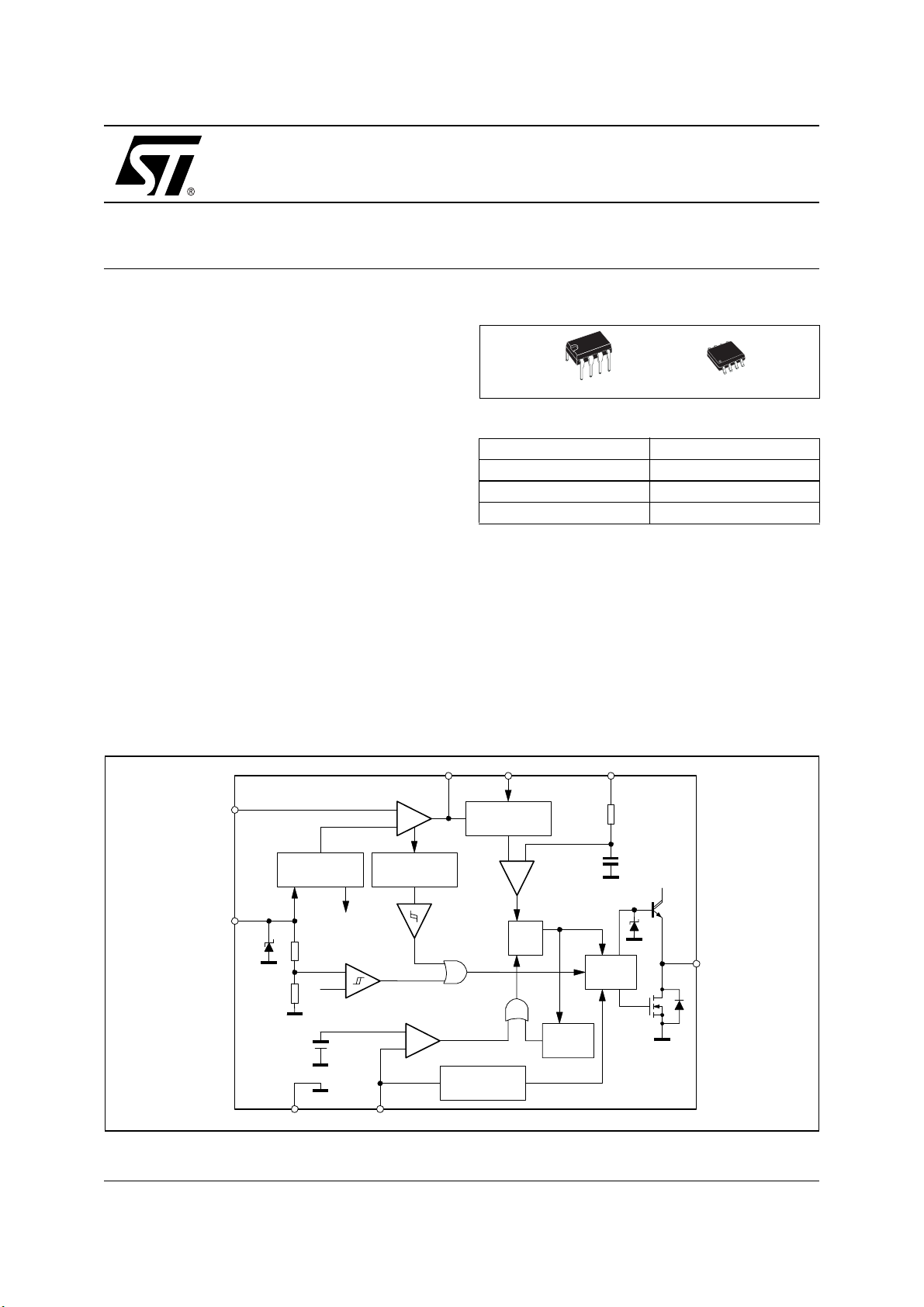
Figure 2. Block Diagram
1
INV
VOLTAGE
REGULATOR
®
-
+
2.5V
OVERVOLTAGE
DETECTION
gure 1. Packages
DIP-8
SO-8
Table 1. Order Codes
Part Number Package
L6562N DIP-8
L6562D SO-8
L6562DTR Tape & Reel
DESKTOP PC, MONITOR) UP TO 300W
– HI-END AC-DC ADAPTER/CHARGER
– ENTRY LEVEL SERVER & WEB SERVER
2 Description
The L6562 is a current-mode PFC controller operating in Transition Mode (TM). Pin-to-pin compatible with the predecessor L6561, it offers improved
performance.
COMP MULT CS
23 4
MULTIPLIER AND
THD OPTIMIZ ER
+
-
40K
5pF
VCC
November 2005
8
V
CC
25 V
R2
6
2.1 V
1.6 V
GND
R1
INTERNAL
SUPPLY 7V
REF2
V
DRIVER
15 V
7
GD
RSQ
+
UVLO
-
ZERO CURRENT
DETECTOR
+
-
5
ZCD
DISABLE
Starter
stop
STARTER
Rev. 8
1/16
L6562
2 Description (continued)
The highly linear multiplier includes a special circuit, able to reduce AC input current distortion, that allows
wide-range-mains operation with an extremely low THD, even over a large load range.
The output voltage is controlled by means of a voltage-mode error amplifier and a precise (1% @Tj =
25°C) internal voltage reference.
The device features extremely low consumption (≤70 µA before start-up and <4 mA running) and includes
a disable function suitable for IC remote ON/OFF, which makes it easier to comply with energy saving
norms (Blue Angel, EnergyStar, Energy2000, etc.).
An effective two-step OVP enables to safely handle overvoltages either occurring at start-up or resulting
from load disconnection.
The totem-pole output stage, capable of 600 mA source and 800 mA sink current, is suitable for big MOSFET or IGBT drive which, combined with the other features, makes the device an excellent low-cost solution for EN61000-3-2 compliant SMPS's up to 300W.
Table 2. Absolute Maximum Ratings
Symbol Pin Parameter Value Unit
V
CC
--- 1 to 4 Analog Inputs & Outputs -0.3 to 8 V
IZCD 5 Zero Current Detector Max. Current -50 (source)
P
tot
T
j
T
stg
8 IC Supply voltage (Icc = 20 mA) self-limited V
10 (sink)
Power Dissipation @Tamb = 50°C (DIP-8)
(SO-8)
Junction Temperature Operating range -40 to 150 °C
Storage Temperature -55 to 150 °C
1
0.65
Figure 3. Pin Connection (Top view)
INV
COMP
MULT
CS
1
2
3
4
Vcc
8
7
GD
GND
6
ZCD
5
Table 3. Thermal Data
mA
W
Symbol Parameter SO8 Minidip Unit
2/16
R
th j-amb
Max. Thermal Resistance, Junction-to-ambient 150 100 °C/W
Table 4. Pin Description
N° Pin Function
1 INV Inverting input of the error amplifier. The information on the output voltage of the PFC pre-
regulator is fed into the pin through a resistor divider.
2 COMP Output of the error amplifier. A compensation network is placed between this pin and INV (pin
#1) to achieve stability of the voltage control loop and ensure high power factor and low THD.
3 MULT Main input to the multiplier. This pin is connected to the rectified mains voltage via a resistor
divider and provides the sinusoidal reference to the current loop.
4 CS Input to the PWM comparator. The current flowing in the MOSFET is sensed through a resistor,
the resulting voltage is applied to this pin and compared with an internal sinusoidal-shaped
reference, generated by the multiplier, to determine MOSFET’s turn-off.
5 ZCD Boost inductor’s demagnetization sensing input for transition-mode operation. A negative-going
edge triggers MOSFET’s turn-on.
6 GND Ground. Current return for both the signal part of the IC and the gate driver.
7 GD Gate driver output. The totem pole output stage is able to drive power MOSFET’s and IGBT’s
with a peak current of 600 mA source and 800 mA sink. The high-level voltage of this pin is
clamped at about 12V to avoid excessive gate voltages in case the pin is supplied with a high
Vcc.
8 Vcc Supply Voltage of both the signal part of the IC and the gate driver. The supply voltage upper
limit is extended to 22V min. to provide more headroom for supply voltage changes.
L6562
Table 5. Electrical Characteristics
= -25 to 125°C, VCC = 12, CO = 1 nF; unless otherwise specified)
(T
j
Symbol Parameter Test Condition Min. Typ. Max. Unit
SUPPLY VOLTAGE
V
V
CCon
V
CCOff
Hys Hysteresis 2.2 2.8 V
V
SUPPLY CURRENT
I
start-up
I
MULTIPLIER INPUT
I
MULT
V
MULT
VCS∆
---------------------
V
∆
MULT
ERROR AMPLIFIER
V
I
Operating range After turn-on 10.3 22 V
CC
Turn-on threshold
Turn-off threshold
Zener Voltage ICC = 20 mA 22 25 28 V
Z
(1)
(1)
11 12 13 V
8.7 9.5 10.3 V
Start-up Current Before turn-on, VCC =11V 40 70 µA
Quiescent Current After turn-on 2.5 3.75 mA
I
q
Operating Supply Current @ 70 kHz 3.5 5 mA
CC
I
Quiescent Current During OVP (either static or
q
Input Bias Current V
dynamic) or V
= 0 to 4 V -1 µA
VFF
=150 mV
ZCD
Linear Operation Range 0 to 3 V
Output Max. Slope V
K
INV
(2)
Gain
Voltage Feedback Input
Threshold
= 0 to 0.5V
MULT
= Upper clamp
V
COMP
V
MULT
= 1 V, V
= 4 V 0.5 0.6 0.7 1/V
COMP
Tj = 25 °C 2.465 2.5 2.535 V
10.3 V < Vcc < 22 V
(1)
1.65 1.9 V/V
2.44 2.56
Line Regulation Vcc = 10.3 V to 22V 2 5 mV
Input Bias Current V
INV
= 0 to 3 V -1 µA
INV
2.2 mA
3/16
L6562
Table 5. Electrical Characteristics (continued)
(T
= -25 to 125°C, VCC = 12, CO = 1 nF; unless otherwise specified)
j
Symbol Parameter Test Condition Min. Typ. Max. Unit
G
GB Gain-Bandwidth Product 1 MHz
I
COMP
V
COMP
CURRENT SENSE COMPARATOR
I
t
d(H-L)
V
CS clamp
V
CSoffset
ZERO CURRENT DETECTOR
V
ZCDH
V
ZCDL
V
ZCDA
V
ZCDT
I
ZCDb
I
ZCDsrc
I
ZCDsnk
V
ZCDdis
V
ZCDen
I
ZCDres
STARTER
t
START
OUTPUT OVERVOLTAGE
I
OVP
Hys Hysteresis
GATE DRIVER
V
V
V
Oclamp
(1) All parameters are in tracking
(2) The multiplier output is given by:
(3) Parameters guaranteed by design, functionality tested in production.
Voltage Gain Open loop 60 80 dB
v
Source Current V
Sink Current V
Upper Clamp Voltage I
Lower Clamp Voltage
Input Bias Current VCS = 0 -1 µA
CS
Delay to Output
Current sense reference clamp V
Current sense offset V
Upper Clamp Voltage I
Lower Clamp Voltage I
Arming Voltage
COMP
COMP
SOURCE
I
= 0.5 mA
SINK
= 4V, V
= 4V, V
= 0.5 mA 5.3 5.7 6 V
= 2.4 V -2 -3.5 -5 mA
INV
= 2.6 V 2.5 4.5 mA
INV
(1)
2.12.252.4 V
200 350 ns
= Upper clamp 1.6 1.7 1.8 V
COMP
= 0 30 mV
MULT
V
= 2.5V 5
MULT
= 2.5 mA 5.0 5.7 6.5 V
ZCD
= -2.5 mA 0.3 0.65 1 V
ZCD
(3)
2.1 V
(positive-going edge)
Triggering Voltage
(3)
1.6 V
(negative-going edge)
Input Bias Current
= 1 to 4.5 V
V
ZCD
2µA
Source Current Capability -2.5 -5.5 mA
Sink Current Capability 2.5 mA
Disable threshold 150 200 250 mV
Restart threshold 350 mV
Restart Current after Disable 30 75 µA
Start Timer period
75 130 300 µs
Dynamic OVP triggering current 35 40 45 µA
(3)
Static OVP threshold
OH
Dropout Voltage
OL
Voltage Fall Time 30 70 ns
t
f
Voltage Rise Time 40 80 ns
t
r
Output clamp voltage I
UVLO saturation V
VcsKV
(1)
I
GDsource
I
GDsource
I
= 200 mA
GDsink
GDsource
= 0 to V
CC
MULTVCOMP
= 20 mA
= 200 mA
= 5mA; Vcc = 20V
, I
CCon
2.5–()⋅⋅=
=10mA 1.1 V
sink
2.12.252.4 V
10 12 15 V
30 µA
22.6
2.5 3 V
0.9 1.9 V
4/16
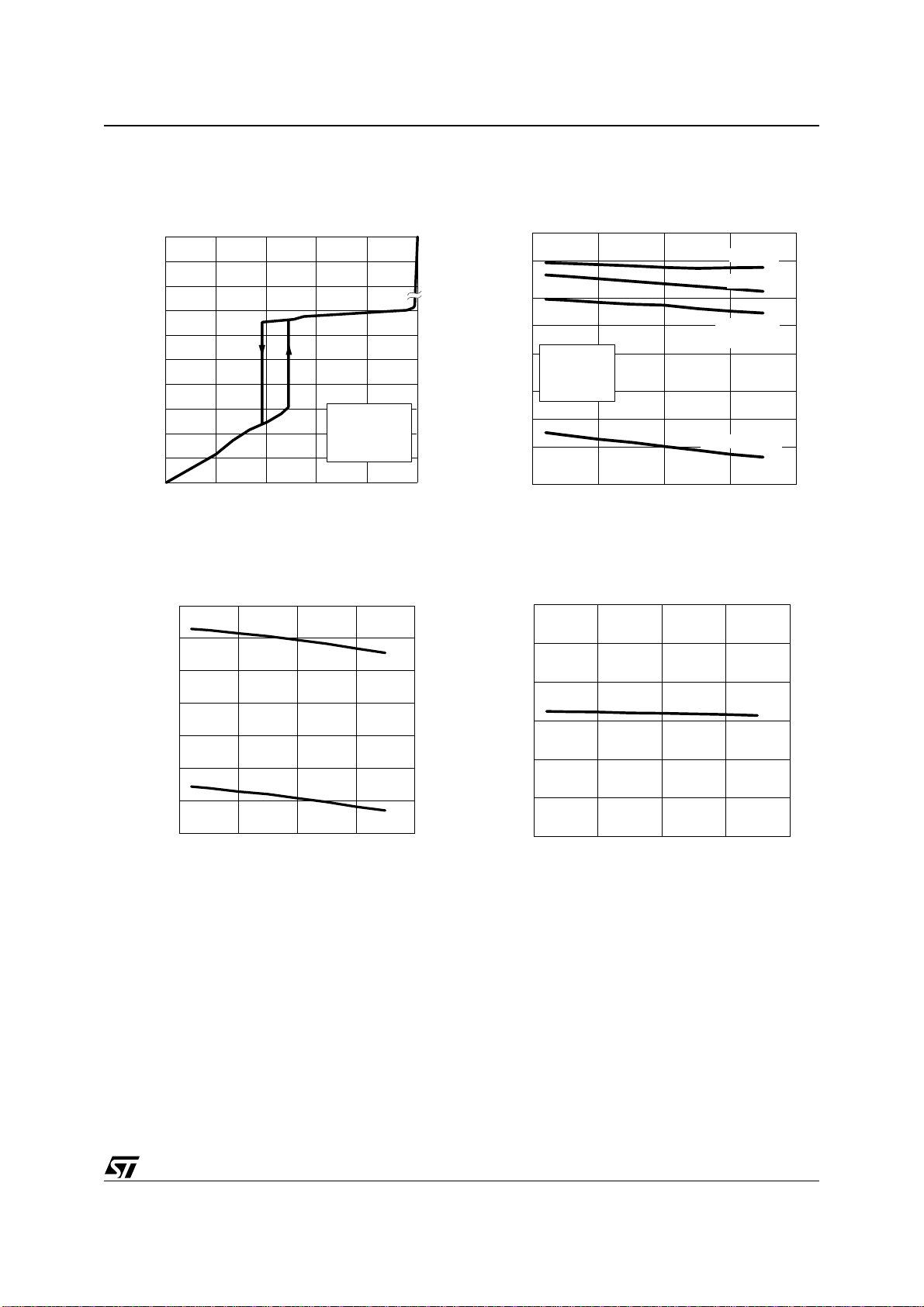
3 Typical Electrical Characteristics
L6562
Figure 4. Supply current vs. Supply voltage
I
CC
(mA)
10
5
1
0.5
0.1
0.05
0.01
0.005
0
0 5 10 15 20
V
cc(V)
Figure 5. Start-up & UVLO vs. T
12.5
V
CC-ON
12
(V)
Co = 1nF
f = 70 kHz
T
= 25°C
j
j
25
Figure 6. IC consumption vs. T
Icc
10
[mA]
5
j
2
1
0.5
Vcc = 12 V
Co = 1 nF
f = 70 kHz
0.2
0.1
0.05
0.02
-50 0 50 100 150
Before start-up
Tj (°C)
Figure 7. Vcc Zener voltage vs. Tj
Vcc
Z
28
(V)
27
Operating
Quiescent
Disabled or
durin g O VP
CC-OFF
V
(V)
11.5
11
10.5
10
9.5
9
-50 0 50 100 150
Tj (
°C)
26
25
24
23
22
-50 0 50 100 150
Tj (°C)
5/16

L6562
Figure 8. Feedback reference vs. Tj
V
REF
2.6
(V)
2.55
2.5
2.45
2.4
-50 0 50 100 150
Tj (°C)
Figure 9. OVP current vs. T
I
OVP
41
(µA)
40.5
40
39.5
39
-50 0 50 100 150
Tj (°C)
j
Vcc = 12 V
Vcc = 12 V
Figure 11. Delay-to-output vs. T
t
D(H-L)
500
(ns)
400
300
200
100
0
-50 0 50 100 150
Tj (°C)
j
Figure 12. Multiplier characteristic
V
(pin 4)
CS
upper voltage
(V)
clamp
1.6
1.4
1.2
1.0
0.8
0.6
0.4
0.2
0
0 0.5 1.0 1.5 2.0 2.5 3.0 3.5 4.0 4.5
5.0
4
5
.
4.0
V
MULT
(pin 3) (V)
Vcc = 12 V
V
COMP
(V)
3.5
3.2
3.0
2.8
2.6
(pin 2)
Figure 10. E/A output clamp levels vs. T
Vpin2
6
(V)
6/16
Upper clamp
5
4
3
Lower clamp
2
-50 0 50 100 150
Tj (°C)
Vcc = 12 V
j
Figure 13. Multiplier gain vs. T
K
1
0.8
j
Vcc = 12 V
V
=4 V
COMP
V
=1V
MULT
0.6
0.4
0.2
0
-50 0 50 100 150
Tj (°C)

L6562
Figure 14. Vcs clamp vs. Tj
V
CSx
2
(V)
1.8
1.6
1.4
Vcc = 12 V
COMP
= Upper cl a m p
V
1.2
1
-50 0 50 100 150
Tj (°C)
Figure 15. Start-up timer vs. T
Tstart
150
(µs)
140
130
Vcc = 12 V
Figure 17. ZCD source capability vs. T
I
ZCDsrc
0
(mA)
-2
-4
-6
-8
-50 0 50 100 150
Tj (°C)
j
Figure 18. Gate-drive output low saturation
pin7
V
[V]
4
Tj = 25 °C
Vcc = 11 V
SINK
Vcc = 12 V
V
= lower clam p
ZCD
j
3
120
110
100
-50 0 50 100 150
Tj (°C)
Figure 16. ZCD clamp levels vs. T
V
ZCD
7
(V)
6
5
4
3
2
1
0
-50 0 50 100 150
Tj (°C)
Upper clamp
I
ZCD
Lower clamp
j
Vcc = 12 V
= ±2.5 mA
2
1
0
0 200 400 600 800 1,000
IGD[mA]
Figure 19. Gate-drive output high saturation
pin7
V
[V]
-1.5
Tj = 25 °C
Vcc - 2.0
-2.5
Vcc - 2.5
Vcc - 3.0
-3.5
Vcc - 3.5
Vcc - 4.0
-4.5
-2
-3
-4
0 100 200 300 400 500 600 700
IGD[mA]
Vcc = 11 V
SOURCE
7/16

L6562
Figure 20. Gate-drive clamp vs. T
clamp
Vpin7
15
(V)
14
13
12
11
10
-50 0 50 100 150
Tj (°C)
j
Vcc = 20 V
Figure 21. UVLO saturation vs. T
Vpin7
1.1
(V)
1
0.9
0.8
0.7
0.6
0.5
-50 0 50 100 150
Tj ( °C )
j
Vcc = 0 V
4 Application Information
4.1 Overvoltage protection
Under steady-state conditions, the voltage control loop keeps the output voltage Vo of a PFC pre-regulator
close to its nominal value, set by the resistors R1 and R2 of the output divider. Neglecting ripple components, the current through R1, I
the error amplifier is internally referenced at 2.5V, also the voltage at pin INV will be 2.5V, then:
, equals that through R2, IR2. Considering that the non-inverting input of
R1
I
R2
2.5
-------- I
R2
R1
Vo 2.5–
--------------------- -===
R1
.
If the output voltage experiences an abrupt change ∆Vo > 0 due to a load drop, the voltage at pin INV will
be kept at 2.5V by the local feedback of the error amplifier, a network connected between pins INV and
COMP that introduces a long time constant to achieve high PF (this is why ∆Vo can be large). As a result,
the current through R2 will remain equal to 2.5/R2 but that through R1 will become:
R1
Vo 2.5– Vo∆+
--------------------------------------- -=
R1
.
I'
The difference current ∆IR1=I'R1-IR2=I'R1-IR1=∆Vo/R1 will flow through the compensation network and enter the error amplifier output (pin COMP). This current is monitored inside the L6562 and if it reaches about
37 µA the output voltage of the multiplier is forced to decrease, thus smoothly reducing the energy delivered to the output. As the current exceeds 40 µA, the OVP is triggered (Dynamic OVP): the gate-drive is
forced low to switch off the external power transistor and the IC put in an idle state. This condition is maintained until the current falls below approximately 10 µA, which re-enables the internal starter and allows
switching to restart. The output ∆Vo that is able to trigger the Dynamic OVP function is then:
Vo∆ R1 40 10
⋅⋅=
6–
.
An important advantage of this technique is that the OV level can be set independently of the regulated
output voltage: the latter depends on the ratio of R1 to R2, the former on the individual value of R1. Another
advantage is the precision: the tolerance of the detection current is 12%, that is 12% tolerance on ∆Vo.
Since ∆Vo << Vo, the tolerance on the absolute value will be proportionally reduced.
Example: Vo = 400 V, ∆Vo = 40 V. Then: R1=40V/40µA=1MΩ; R2=1MΩ·2.5/(400-2.5)=6.289kΩ. The tol-
erance on the OVP level due to the L6562 will be 40·0.12=4.8V, that is 1.2% of the regulated value.
8/16

L6562
When the load of a PFC pre-regulator is very low, the output voltage tends to stay steadily above the nominal value, which cannot be handled by the Dynamic OVP. If this occurs, however, the error amplifier output will saturate low; hence, when this is detected, the external power transistor is switched off and the IC
put in an idle state (Static OVP). Normal operation is resumed as the error amplifier goes back into its linear region. As a result, the L6562 will work in burst-mode, with a repetition rate that can be very low.
When either OVP is activated the quiescent consumption of the IC is reduced to minimize the discharge
of the Vcc capacitor and increase the hold-up capability of the IC supply system.
4.2 THD optimizer circuit
The L6562 is equipped with a special circuit that reduces the conduction dead-angle occurring to the AC
input current near the zero-crossings of the line voltage (crossover distortion). In this way the THD (Total
Harmonic Distortion) of the current is considerably reduced.
A major cause of this distortion is the inability of the system to transfer energy effectively when the instantaneous line voltage is very low. This effect is magnified by the high-frequency filter capacitor placed after
the bridge rectifier, which retains some residual voltage that causes the diodes of the bridge rectifier to be
reverse-biased and the input current flow to temporarily stop.
Figure 22. THD optimization: standard TM PFC controller (left side) and L6562 (right side)
Input current Input current
Rectified mains voltage Rectified mains voltage
Imains
Input current
MOSFET's drain voltage
Vdrain
Imains
Input current
MOSFET's drain voltage
Vdrain
To overcome this issue the circuit embedded in the L6562 forces the PFC pre-regulator to process more
energy near the line voltage zero-crossings as compared to that commanded by the control loop. This will
result in both minimizing the time interval where energy transfer is lacking and fully discharging the highfrequency filter capacitor after the bridge. The effect of the circuit is shown in figure 23, where the key
waveforms of a standard TM PFC controller are compared to those of the L6562.
Essentially, the circuit artificially increases the ON-time of the power switch with a positive offset added to
9/16

L6562
the output of the multiplier in the proximity of the line voltage zero-crossings. This offset is reduced as the
instantaneous line voltage increases, so that it becomes negligible as the line voltage moves toward the
top of the sinusoid.
To maximally benefit from the THD optimizer circuit, the high-frequency filter capacitor after the bridge rectifier should be minimized, compatibly with EMI filtering needs. A large capacitance, in fact, introduces a
conduction dead-angle of the AC input current in itself - even with an ideal energy transfer by the PFC preregulator - thus making the action of the optimizer circuit little effective.
Figure 23. Typical application circuit (250W, Wide-range mains)
D3 1N5406
T
C23
680 nF
5
21
L6562
6
R50 10 k
C3 2.2 µF
4
NTC
D1
1W
MOS
Ω
2.5 Ω
R13
9.53 kΩ
STTH5L06
Ω
R7
10
Ω
7
0.33
R9
1W
Ω
STP12NM50
7 °C/W heat sink
R10
0.33
R11
750 kΩ
R12
750 k
Vo=400V
Po=250W
Ω
C6
100 µF
450V
-
5A/250V
Vac
(85V to 265V)
FUSE
+
-
BRIDGE
STBR606
C1
1 µF
400V
22 kΩ
R4
R5
D8
180 kΩ
180 kΩ
R1
1.5 MΩ
R2
1.5 MΩ
C2
10nF
R3
C29
22 µF
25V
1N4150
D2
1N5248B
C5 12 nF
C4
100 nF
R14
100 Ω
R6
68 kΩ
8
3
Boost In ductor Spec: EB 0057-C (CO ILCRAFT)
Figure 24. Demo board (EVAL6562-80W, Wide-range mains): Electrical schematic
Ω
5
21
L6562
6
T
330 nF
R50 12 kΩ
C3 680 nF
C23
4
D1
STTH1L06
R7
Ω
33
7
R9
0.82
0.6 W
STP8NM50
Ω
MOS
R10
0.82
0.6 W
9.53 k
Ω
4A/250V
Vac
(85V to 265V)
FUSE
R4
180 kΩ
R1
750 kΩ
BRIDGE
DF06M
+
-
Boost Ind uctor Spec (ITACOIL E2543/E)
C1
0.47 µF
400V
R2
750 k
Ω
C2
10nF
R3
10 kΩ
E25x13x7 core, 3C 85 ferrite
1.5 mm ga p for 0.7 mH primar y inductance
Primary: 105 turns 20 x0.1 mm
Secondary: 11 turns 0.1 mm
180 k
22 µF
R5
C29
25V
Ω
D8
1N4150
D2
1N5248B
C5 12 nF
C4
100 nF
R14
100 Ω
R6
68 k
8
3
NTC
2.5 Ω
R13
Vo=400V
R11
Po=80W
Ω
750 k
R12
750 k
Ω
C6
47 µF
450V
Ω
-
10/16

Figure 25. EVAL6562-80W: PCB and component layout (Top view, real size: 57 x 108 mm)
L6562
Table 6. EVAL6562N: Evaluation results at full load
Vin (VAC)
Pin (W)
85 86.4 394.79 12.8 80.16 92.8 0.998 3.6
110 84.6 394.86 12.8 80.20 94.8 0.996 4.2
135 83.8 394.86 12.8 80.20 95.7 0.991 4.9
175 83.2 394.87 15.5 80.20 96.4 0.981 6.5
220 82.9 394.87 15.7 80.20 96.7 0.956 7.8
265 82.7 394.87 15.9 80.20 97.0 0.915 9.2
Note: measurements done with the line filter shown in figure 23
Vo (V
) ∆Vo(V
DC
pk-pk
)
Po (W) η (%) PF THD (%)
Table 7. EVAL6562N: Evaluation results at half load
Vin (VAC)
Pin (W)
85 42.8 394.86 6.6 40.20 93.9 0.994 5.5
110 42.5 394.90 6.6 40.20 94.6 0.985 6.2
135 42.5 394.91 6.7 40.20 94.6 0.967 7.1
175 42.5 394.93 8.0 40.19 94.6 0.939 8.3
Vo (V
) ∆Vo(V
DC
pk-pk
)
Po (W) η (%) PF THD (%)
220 42.6 394.94 8.2 40.19 94.3 0.869 9.8
265 42.6 394.94 8.3 40.19 94.3 0.776 11.4
Note: measurements done with the line filter shown in figure 23
11/16

L6562
Table 8. EVAL6562N: No-load measurements
Vin (VAC)
Pin (W)
Vo ( V
) ∆Vo(V
DC
pk-pk
)
85 0.4 396.77 0.45 0
110 0.3 396.82 0.55 0
135 0.3 396.83 0.60 0
(*)
175
(*)
220
(*)
265
(*)
Vcc = 12V supplied externally
0.4 396.90 1.00 0
0.4 396.95 1.40 0
0.5 396.98 1.65 0
Figure 26. Line filter (not tested for EMI compliance) used for EVAL6562N evaluation
to the AC
source
B81133
470 nF, X2
EPCOS
B82732
47 mH, 1.3A
EPCOS
B81133
680 nF, X2
EPCOS
to
EVAL6562N
Po (W)
12/16

L6562
5 Package Information
In order to meet environmental requirements, ST offers these devices in ECOPACK® packages. These
packages have a Lead-free second level interconnect. The category of second Level Interconnect is
marked on the package and on the inner box label, in compliance with JEDEC Standard JESD97. The
maximum ratings related to soldering conditions are also marked on the inner box label. ECOPACK is an
ST trademark.
ECOPACK specifications are available at: www.st.com.
Figure 27. DIP-8 Mechanical Data & Package Dimensions
DIM.
A3.32 0.131
a1 0.51 0.020
B 1.15 1.65 0.045 0.065
b 0.356 0.55 0.014 0.022
b1 0.204 0.304 0.008 0.012
D 10.92 0.430
E 7.95 9.75 0.313 0.384
e2.54 0.100
e3 7.62 0.300
e4 7.62 0.300
F 6.6 0.260
I 5.08 0.200
L 3.18 3.81 0.125 0.150
Z 1.52 0.060
mm inch
MIN. TYP. MAX. MIN. TYP. MAX.
OUTLINE AND
MECHANICAL DATA
DIP-8
13/16

L6562
Figure 28. SO-8 Mechanical Data & Package Dimensions
DIM.
A 1.35 1.75 0.053 0.069
A1 0.10 0.25 0.004 0.010
A2 1.10 1.65 0.043 0.065
B 0.33 0.51 0.013 0.020
C 0.19 0.25 0.007 0.010
(1)
D
E 3.80 4.00 0.15 0.157
e 1.27 0.050
H 5.80 6.20 0.228 0.244
h 0 .25 0.50 0.010 0.020
L 0 .40 1.27 0.016 0.050
k 0˚ (min.), 8˚ (max.)
ddd 0.10 0.004
Note: (1) Dimensions D does not in clude mold flash, protru-
mm inch
MIN. TYP. MAX. MIN. TYP. MA X.
4.80 5.00 0.189 0.197
sions or gate burrs.
Mold flash, potrusions or gate burr s shall not ex ceed
0.15mm (.006inch) in total (both side).
OUTLINE AND
MECHANICAL DATA
SO-8
14/16
0016023 C

6 Revision History
Table 9. Revision History
Date Revision Description of Changes
January 2004 5 First Issue
June 2004 6 Modified the Style-look in compliance with the “Corporate Technical
Publications Design Guide”.
Changed input of the power amplifier connected to Multiplier (Fig. 2).
May 2005 7 Modified Table 2: Absolute Maximim Ratings.
L6562
November 2005 8
Added in Section 5 the ECOPACK
®
certicate of conformity.
15/16

L6562
Information furnished is believed to be accurate and reliable. However, STMicroelectronics assumes no responsibility for the consequences
of use of such information nor for any infringement of patents or other rights of third parties which may result from its use. No license is granted
by implication or otherwise under any patent or patent rights of STMicroelectronics. Specifications mentioned in this publication are subject
to change without notice. This publication supersedes and replaces all information previously supplied. STMicroelectronics products are not
authorized for use as critical components in life support devices or systems without express written approval of STMicroelectronics.
The ST logo is a registered trademark of STMicroelectronics.
All other names are the property of their respective owners
© 2005 STMicroelectronics - All rights reserved
Australia - Belgium - Brazil - Canada - China - Czech Republic - Finland - France - Germany - Hong Kong - India - Israel - Italy - Japan -
Malaysia - Malta - Morocco - Singapore - Spain - Sweden - Switzerland - United Kingdom - United States of America
STMicroelectronics group of companies
www.st.com
16/16
 Loading...