

查询L6560供应商
L6560
VERY PRECISE ADJUSTABLE INTERNAL
OUTPUTOVERVOLTAGEPROTECTION
HYSTERETICSTART-UP
(I
START-UP <0.5mA)
VERYLOW QUIESCENTCURRENT
(< 3.5mA)
INTERNALSTART-UP TIMER
TRANSITIONMODE OPERATING
TOTEMPOLEOUTPUTCURRENT:±400mA
DIP8/SO8PACKAGES
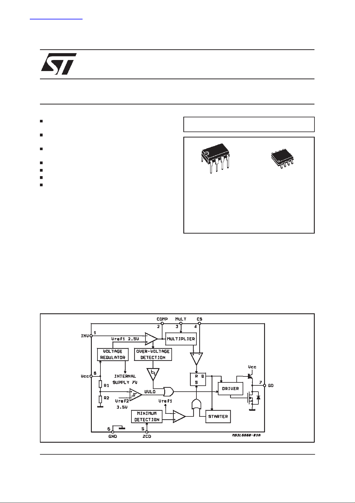
DESCRIPTION
The L6560/A is a monolithic integrated circuit in
Minidip and SO8 packages, designed as a controller and driver of a discrete powerMOS transistor for the implementation of active power factor
correction, for sinusoidal line current consumption.
Realized in mixed BCD technology, the chip integrates:
- An undervoltagelockout with micropowerstartup andhyster es i s .
- An internal temperature compensated precise
bandgap reference.
- A stableerroramplifier.
L6560A
POWER FACTOR CORRECTOR
MULTIPOWER BCD TECHNOLOGY
Minidip SO8
ORDERING NUMBERS:
L6560 L6560D
L6560A L6560AD
- One quadrant multiplier.
- Current sense comparator.
- An output overvoltage protectioncircuit.
- A totem-pole output stage able to drive a
POWER MOS or IGBT devices with source
and sink current of 400mA. The chip works in
transition mode and is particularly intended
for lamp ballast applications and for low
powerSMPS.
BLOCK DIAGRAM
June 2000
1/11
L6560 - L6560A
ABSOLUTE MAXIMUM RATINGS
Symbol Pin Parameter Value Unit
cc
I
V
I
GD
INV, COMP
8ICC+I
Z
7 Output Totem Pole Peak Current (2µs)
1, 2, 3 Analog Inputs & Outputs -0.3 to 7 V
MULT
CS 4 Current Sense Input -0.3 to 7 V
ZCD 5 Zero Current Detector 5 (source)
P
tot
Power Dissipation @T
=50°C (Minidip)
amb
(SO8)
T
j
T
stg
Junction Temperature Operating Range -25 to 150 °C
Storage Temperature -55 to 150 °C
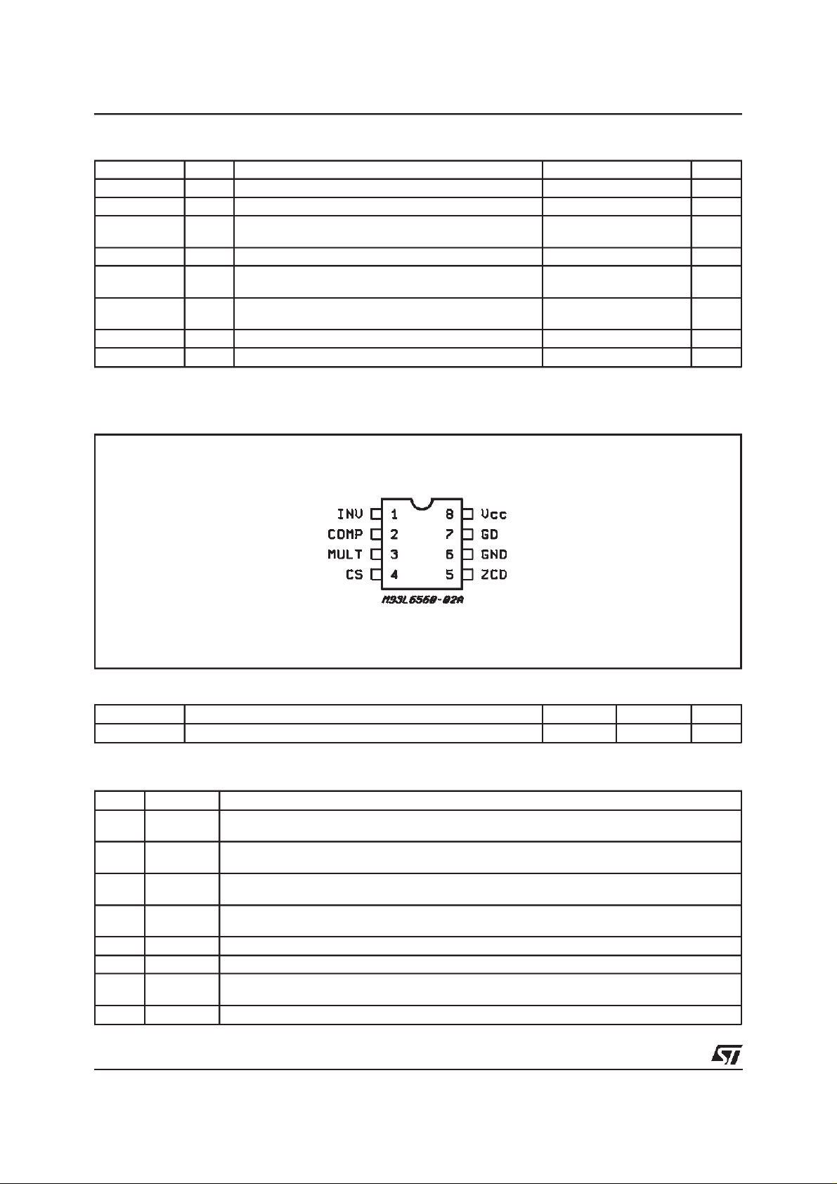
PIN CONNECTION
30 mA
700 mA
±
10 (sink)
1
0.65
mA
mA
W
THERMAL DATA
Symbol Parameter SO 8 MINIDIP Unit
R
th j-amb
Thermal Resistance Junction-ambient 150 100
PIN FUNCTIONS
N. Name Function
1 INV Inverting input of the error amplifier. A resistive divider is connected betweenoutput regulated
2 COMP Output of error amplifier. A feedback compensation network is placed between this pin and the
3 MULT Input of themultipler stage. A resistive divider connects to this pin the rectified mains. A
4 CS Input to the comparator of the control loop. The current is sensed by a resistor and the
5 ZCD Zero current detection input.
6 GND Ground of the control section.
7 GD Gate driver output. A push pull output stage is able to drive the Power MOS with peak current
8V
CC
2/11
voltage and this point, to provide the voltage feedback.
INV pin.
voltage signal, proportional to the rectified mains, appears on this pin.
resulting voltage is applied to this pin.
of 400mA (source and sink).
Supply voltage of driver and control circuits.
C/W
°
L6560 - L6560A
ELECTRICALCHARACTERISTICS
= 14.5V; Tj=25°C unless otherwisespecified)
(V
CC
SUPPLY VOLTAGESECTION
Symbol Pin Parameter Test Condition Min. Typ. Max. Unit
V
CC
V
CC ON
V
CC OFF 8 Turn-off Threshold
8 Operating Range after turn-on 11 18 V
8 Turn-onThreshold L6560
L6560A
13.51114.51215.5
13
L6560
L6560A98.7109.61110.5
Hys 8 Hysteresis L6560
L6560A
4.3
2.5
4.7
2.8
5.1
3.1
SUPPLY CURRENT SECTION
Symbol Pin Parameter Test Condition Min. Typ. Max. Unit
START-U 8 Start-up Current before turn-on at:
I
I
CC
Z 8 Zener Voltage ICC = 25mA 18 20 22 V
V
8 Operating Supply Current CL= 0nF @ 70KHz 2.5 3.5 mA
V
= 13V (L6560)
CC
V
= 10.5V (L6560A)
CC
= 1nF @ 70KHz 3.2 4 mA
C
L
in OVP condition V
= 2.7V 0.9 1.3 mA
pin1
0.3 0.5 mA
ERROR AMPLIFIER SECTION
V
v
V
V
V
V
Symbol Pin Parameter Test Condition Min. Typ. Max. Unit
INV 1 Voltage Feedback Input
V
Threshold
T
R
I
INV
G
I
COMP
S
L
V
Temperature Stability T
Line Regulation VCC= 11 to 18V 1 4 mV
1 Input Bias Current 0.1 1 µA
Voltage Gain Open loop 60 80 dB
2 Source Current (V1<V
Sink Current (V
–25≤T
)V
ref
) 0.5 1 mA
1>Vref
≤85°C;12V< VCC<18V 2.43 2.56
J
= -25 to 85°C 0.5 %
amb
= 5V 0.14 0.2 mA
COMP
2.46 2.5 2.54 V
MULTIPLIERSECTION
Symbol Pin Parameter Test Condition Min. Typ. Max. Unit
V
MULT
∆V
CS
V
∆
mult
K Gain V
3 Operating Voltage 0to 2.5 0to 4.2 V
Output Max. Slope V
= from 0V to 1V
MULT
V
=6V
COMP
=1V V
MULT
0.9 1.25 1.6
= 5V 0.45 0.65 0.85 1/V
COMP
CURRENT SENSE COMPARATOR
Symbol Pin Parameter Test Condition Min. Typ. Max. Unit
CS 4 Voltage Threshold V
V
CS 4 Input Bias Current 5 µA
I
t
d (H-L)
4 Delay to Output 200 400 ns
MULT
= 2.5V V
= 6V 1.6 1.9 V
COMP
3/11
L6560 - L6560A
ELECTRICALCHARACTERISTICS
(continued)
ZERO CURRENT DETECTOR
Symbol Pin Parameter Test Condition Min. Typ. Max. Unit
V
ZCD
V
ZCD
V
ZCD
5 Input Threshold Voltage Rising
Edge
Hysteresis 0.3 0.5 0.7 V
5 Clamp Voltage I
5 Clamp Voltage I
= 3mA 5 5.7 6.4 V
ZCD
= –3mA 0.4 0.7 1 V
ZCD
1.8 2.3 V
OUTPUT SECTION
Symbol Pin Parameter Test Condition Min. Typ. Max. Unit
GD 7 Dropout Voltage IGDsource = 200mA 1.2 2 V
V
GDsource = 20mA 0.7 1 V
I
= 200mA 1.5 V
I
GDsink
= 20mA 0.3 V
I
GDsink
t
r
t
f
7 Output Voltage Rise Time CL = 1nF 50 120 ns
7 Output Voltage Fall Time CL = 1nF 40 100 ns
OUTPUT OVERVOLTAGE SECTION
Symbol Pin Parameter Test Condition Min. Typ. Max. Unit
I
OVP
2 OVP Triggering Current 36 40 44
RESTART TIMER
A
µ
Symbol Pin Parameter Test Condition Min. Typ. Max. Unit
t
START
OVER VOLTAGEPROTECTION OVP
The output voltage is expected to be kept by the
operation of the PFC circuits close to its reference
value that is set by the ratio of the twoexternal resistors R
1 and R2 (see fig. 2), taking into consid-
eration that the non inverting input of the error
amplifier is biased inside the L6560 at 2.5V.
In steady state conditions, the current through R1
and R2 is:
and, if the external compensation network is
made only with a capacitorC, the current through
C is equalzero.
When the output voltage increases abruptly the
current throughR1 becomes:
Start Timer 45 60 µs
+∆V
V
outsc
=
I
R1
R1
OUT
− 2.5
=
+∆
I
sc
Since the current through R2 doesn’t change, the
∆I current must flow through the capacitorC and
enter in the error amplifier.
This current is mirrored inside the L6560, and
compared with a precise internal reference of
40µA. Whenever such 40µA limit is exceed, the
OVP protection is triggered (Dynamic OVP), and
outsc
SC
R1
=
− 2.5
2.5
R2
∆V
=
I
SC
or I
the external power transistor is switched off, until
the overvoltage situation disappears. However if
the overvoltage persists, before that the transient
condition of dynamic circuit exhausts, an internal
comparator (Static OVP) latches the OVP condition keeping the external power switch turned off
(see fig. 1).
The OVP value is threfore set by the equation
1 ⋅
OVP= ∆Vout = R
Typical values for R
40µA.
1,R2and C are reported in
the application circuit. The overvoltage can be set
independently from the average output voltage.
The precision in setting the overvoltage threshold
R1
out
=
R1
I
−2.5
V
is 7% of the overvoltage value (for instance ∆V=
60V ± 4.2V).
I.
4/11

Figure 1.
V
OUT nominal
40µA
I
SC
E/A OUTPUT
3.1V
DYNAMIC OVP
L6560 - L6560A
OVER VOLTAGE
STATIC OVP
Figure 2: OvervoltageProtection Circuit
Ccomp.
+Vo
R1
1
-
E/A
R2
+
2.5V
∆I
40µA
3.1V
D95IN219A
∆I
2
X PWM
DRIVER
-
+
D93IN035B
5/11

L6560 - L6560A
Figure 3:
FUSE 4A/250V
Vac
(85V to 135V)
Typical Application Circuit (100W)
R3
D3 1N4150
68K 5%
BRIDGE
4 x BY255
+
-
TRANSFORMER
T: core THOMSON-CSF B1ET2910A (ETD 29x 16 x 10mm) OR EQUIVALENT
primary 90T of Litz wire 10 x 0.2mm
secondary 11T of #27 AWG (0.15mm)
gap 1.9mm for a total primary inductance of 0.6mH
C1
1µF
250V
R9
1.5M
1%
R10
16K
1%
D2
1N5248B
C2
22µF
25V
R2
100 5%
C7
10nF
R1 68K 5%
8
3
C6
10nF
6
5
L6560
T
C3 330nF
21
4
C4
1nF
R5 10 MOS
7
R4 330
D1 BYT03-400
R6
0.33
1W
1.5M
IRF740
R8
16K
1%
D94IN050B
1%
R7
+
Vo=240V
Po=100W
C5
150µF
315V
-
Figure 4:
FUSE 4A/250V
Vac
(175V to 265V)
Typical Application Circuit (120W)
R3
D3 1N4150
220K 5%
BRIDGE
4 x BY255
+
-
TRANSFORMER
T: core THOMSON-CSF B1ET2910A (ETD29 x 16 x 10mm) OR EQUIVALENT
primary 90T of Litz wire 10 x 0.2mm
secondary 7T of #27 AWG (0.15mm)
gap 1.25mmfor a total primary inductance of 0.8mH
C1
1µF
400V
R9
1.8M
1%
R10
6.2K
1%
D2
1N5248B
C2
22µF
25V
R2
100 5%
R1 68K 5%
C7
10nF
8
3
C6
4.7nF
6
5
L6560
T
C3 1µF
21
4
C4
1nF
R5 10 MOS
7
R4 330
D1 BYT13-600
STP8NA50
R6
0.4
1W
R7
1M
1%
R8
6.34K
1%
D94IN049A
+
Vo=400V
Po=120W
C5
47µF
450V
-
6/11
L6560 - L6560A
Figure 5:
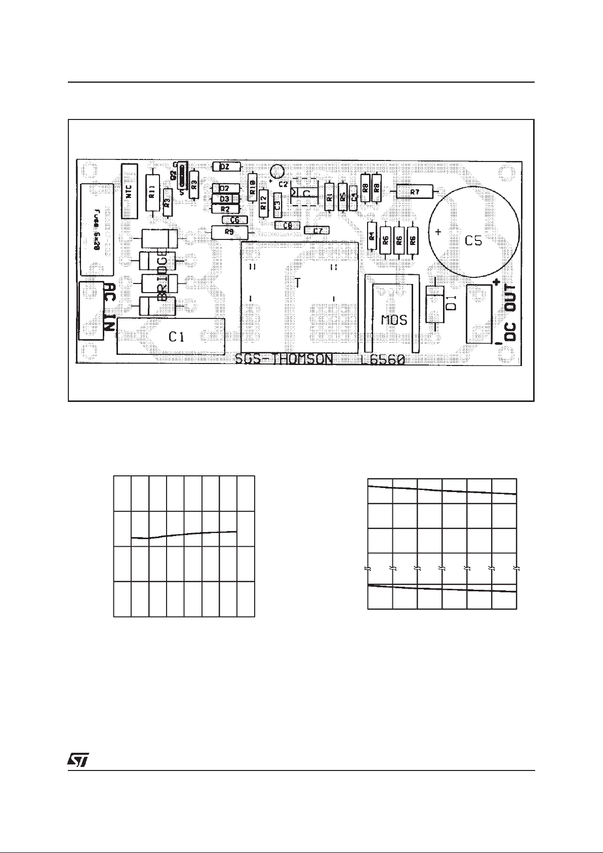
P.C.Boardand ComponentLayout of the Figg. 3 and 4 (1:1.25 scale)
Figure6: OVPCurrentThresholdvs.Temperature
I
OVP
(mA)
42
41
40
39
-50 -25 0 25 50 75 100 125 T (°C)
D94IN047
Figure7
V
CC-TH-ON
(V)
V
CC-TH-OFF
(V)
: UndervoltageLockout Threshold vs.
Temperature
D94IN044
14
13
12
10
9
-25 0 25 50 75 100 125
T(°C)
7/11

L6560 - L6560A
Figure 8: Supply Current vs. SupplyVoltage
ICC
(mA)
4
3
2
1
0
-5 0 5 10 15 20 VCC(V)
Figure 10
CL=
1nF
f=
70KHz
TA=25°C
: Output SaturationVoltage vs. Sink
D94IN045
Current
V
PIN7
(V)
2.0
VCC= 14.5V
D94IN046
SINK
Figure9: VoltageFeedbackInput Thresholdvs.
Temperature
V
REF
(V)
2.50
2.48
2.46
Figure11
-50 0 50 100
: Output SaturationVoltage vs. Source
D94IN048
T(°C)
Current
V
PIN7
(V)
VCC-0.5
VCC= 14.5V
D94IN053
1.5
1.0
0.5
0
Figure 12
V
(pin4)
CS
(V)
1.8
1.6
1.4
1.2
1.0
0.8
0.6
0.4
0.2
0.0
8/11
0 100 200 300 400 IGD(mA)
: MultiplierCharacteristicsFamily
V
D94IN042
-1.0 0.0 1.0 2.0 3.0
VMULT(pin3) (V)
COMP
4.0 5.0
(pin2)
(V)
5.7
5.1
4.7
4.3
4.1
3.9
3.7
3.6
VCC-1.0
VCC-1.5
VCC-2.0
0
Figure13
VCS(pin4)
(mV)
550
500
450
400
350
300
250
200
150
100
50
0
SOURCE
0 100 200 300 400 IGD(mA)
: MultiplierCharacteristicsFamily
V
D94IN043
-200 -100 0 100 200 300 400
V
(pin3) (mV)
MULT
COMP
5.7
5.1
4.7
4.3
4.1
3.9
3.7
3.6

L6560 - L6560A
DIM.
MIN. TYP. MAX. MIN. TYP. MAX.
A 3.32 0.131
a1 0.51 0.020
B 1.15 1.65 0.045 0.065
b 0.356 0.55 0.014 0.022
b1 0.204 0.304 0.008 0.012
D 10.92 0.430
E 7.95 9.75 0.313 0.384
e 2.54 0.100
e3 7.62 0.300
e4 7.62 0.300
F 6.6 0.260
I 5.08 0.200
L 3.18 3.81 0.125 0.150
Z 1.52 0.060
mm inch
OUTLINE AND
MECHANICAL DATA
Minidip
9/11

L6560 - L6560A
DIM.
MIN. TYP. MAX. MIN. TYP. MAX.
A 1.75 0.069
a1 0.1 0.25 0.004 0.010
a2 1.65 0.065
a3 0.65 0.85 0.026 0.033
b 0.35 0.48 0.014 0.019
b1 0.19 0.25 0.007 0.010
C 0.25 0.5 0.010 0.020
c1 45° (typ.)
D (1) 4.8 5.0 0.189 0.197
E 5.8 6.2 0.228 0.244
e 1.27 0.050
e3 3.81 0.150
F (1) 3.8 4.0 0.15 0.157
L 0.4 1.27 0.016 0.050
M 0.6 0.024
S8°(max.)
(1) D andF do notinclude mold flash or protrusions. Moldflash or
potrusions shall not exceed 0.15mm(.006inch).
mm inch
OUTLINE AND
MECHANICAL DATA
SO8
10/11

L6560 - L6560A
Information furnished is believed to be accurate and reliable. However,STMicroelectronics assumes no responsibility for the consequences
of use of such information nor for any infringement of patents or other rights of third parties which may result from its use. No license is
granted by implication or otherwise under any patent or patent rights of STMicroelectronics. Specification mentioned in this publication are
subject to change without notice. This publication supersedes and replaces all information previously supplied. STMicroelectronics products
are not authorized for use as critical components in life support devices or systems without express written approval of STMicroelectronics.
Australia - Brazil - China- Finland - France - Germany - Hong Kong - India - Italy - Japan - Malaysia - Malta - Morocco -
The ST logo is a registered trademark of STMicroelectronics
2000 STMicroelectronics – Printed in Italy – AllRights Reserved
Singapore - Spain - Sweden - Switzerland - United Kingdom - U.S.A.
STMicroelectronics GROUP OF COMPANIES
http://www.st.com
11/11
 Loading...