

SPI configurable stepper and DC multi motor driver
Features
■ Operating supply voltage from 13 V to 38 V
■ 4 full bridge driver configurable in multi-motor
application to drive:
– 2 DC and 1 stepper motor
–4 DC motor
■ Bridge 1 and 2 (R
configured to work as:
– Dual full bridge driver
– Super DC driver
– 2 half bridge driver
– 1 super half bridge
–2 power switches
– 1 super power switch
■ Bridge 3 and 4 (R
configured to work as:
– Same as bridges 1 and 2, listed above
– Stepper motor driver: up to 1/16
microstepping
– 2 buck regulators (bridge 3)
– 1 super buck regulator
– Battery charger (bridge 4)
■ Power supply management
– One switching buck regulator
– One switching regulator controller
– One linear regulator
– One battery charger
■ Fully protected through
– Thermal warning and shutdown
– Overcurrent protection
– Undervoltage lock-out
■ SPI interface
■ Programmable watchdog function
■ Integrated power sequencing and supervisory
functions with fault signaling through serial
interface and external reset pin
■ Very low power dissipation in shut-down mode
(~35 mW)
= 0.60 Ω) can be
DSon
= 0.85 Ω) can be
DSon
L6460
TQFP64 exposed pad
■ Auxiliary features
– Multi-channels 9 bit ADC
– 2 operational amplifiers
– Digital comparator
– 2 low voltage power switches
– 3 general purpose PWM generators
–14 GPIOs
Description
The L6460 is optimized to control and drive multimotor system providing a unique level of
integration in term of control, power and auxiliary
features. Thanks to the high configurability L6460
can be customized to drive different motor
architectures and to optimize the number of
embedded features, such as the voltage
regulators, the high precision A/D converter, the
operational amplifier and the voltage
comparators. The possibility to drive
simultaneously stepper and DC motor makes
L6460 the ideal solution for all the application
featuring multi motors.
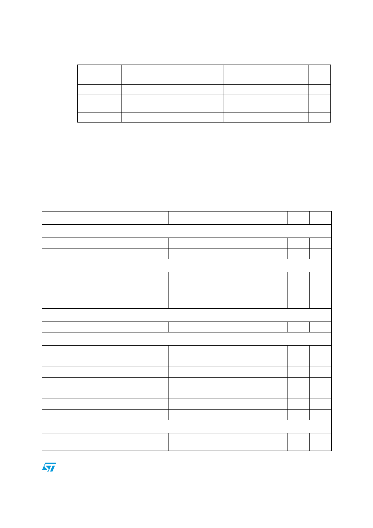
Table 1. Device summary
Order code Package Packing
L6460
TQFP64
L6460TR Tape and reel
Tr ay
July 2010 Doc ID 17713 Rev 1 1/139
www.st.com
139

Contents L6460
Contents
1 General description . . . . . . . . . . . . . . . . . . . . . . . . . . . . . . . . . . . . . . . . . 10
1.1 Overview . . . . . . . . . . . . . . . . . . . . . . . . . . . . . . . . . . . . . . . . . . . . . . . . . 10
1.2 Pin connection . . . . . . . . . . . . . . . . . . . . . . . . . . . . . . . . . . . . . . . . . . . . . 11
1.3 Pin list . . . . . . . . . . . . . . . . . . . . . . . . . . . . . . . . . . . . . . . . . . . . . . . . . . . . 12
2 L6460’s main features . . . . . . . . . . . . . . . . . . . . . . . . . . . . . . . . . . . . . . . 14
3 Electrical specifications . . . . . . . . . . . . . . . . . . . . . . . . . . . . . . . . . . . . . 16
3.1 Absolute maximum rating . . . . . . . . . . . . . . . . . . . . . . . . . . . . . . . . . . . . . 16
3.2 Operating ratings specifications . . . . . . . . . . . . . . . . . . . . . . . . . . . . . . . . 16
3.3 Electrical characteristics . . . . . . . . . . . . . . . . . . . . . . . . . . . . . . . . . . . . . . 17
4 Internal supplies . . . . . . . . . . . . . . . . . . . . . . . . . . . . . . . . . . . . . . . . . . . 30
4.1 V
SupplyInt
regulator . . . . . . . . . . . . . . . . . . . . . . . . . . . . . . . . . . . . . . . . . . 30
4.2 Charge pump regulator . . . . . . . . . . . . . . . . . . . . . . . . . . . . . . . . . . . . . . 31
4.3 V3v3 regulator . . . . . . . . . . . . . . . . . . . . . . . . . . . . . . . . . . . . . . . . . . . . . 31
5 Supervisory system . . . . . . . . . . . . . . . . . . . . . . . . . . . . . . . . . . . . . . . . 32
5.1 Power on reset (POR) circuit . . . . . . . . . . . . . . . . . . . . . . . . . . . . . . . . . . 32
5.2 nRESET generation circuit . . . . . . . . . . . . . . . . . . . . . . . . . . . . . . . . . . . . 32
5.3 Thermal shut down generation circuit . . . . . . . . . . . . . . . . . . . . . . . . . . . 35
6 Watchdog circuit . . . . . . . . . . . . . . . . . . . . . . . . . . . . . . . . . . . . . . . . . . . 36
7 Internal clock oscillator . . . . . . . . . . . . . . . . . . . . . . . . . . . . . . . . . . . . . 38
8 Start-up configurations . . . . . . . . . . . . . . . . . . . . . . . . . . . . . . . . . . . . . 39
8.1 Operation modes . . . . . . . . . . . . . . . . . . . . . . . . . . . . . . . . . . . . . . . . . . . 39
8.2 Basic device mode . . . . . . . . . . . . . . . . . . . . . . . . . . . . . . . . . . . . . . . . . . 40
8.3 Slave device mode . . . . . . . . . . . . . . . . . . . . . . . . . . . . . . . . . . . . . . . . . . 41
8.4 Master device mode . . . . . . . . . . . . . . . . . . . . . . . . . . . . . . . . . . . . . . . . . 41
8.5 Single device mode . . . . . . . . . . . . . . . . . . . . . . . . . . . . . . . . . . . . . . . . . 41
8.6 Sub-configurations for slave, master or single device modes . . . . . . . . . 41
2/139 Doc ID 17713 Rev 1

L6460 Contents
8.6.1 Bridge mode . . . . . . . . . . . . . . . . . . . . . . . . . . . . . . . . . . . . . . . . . . . . . 41
8.6.2 Primary regulator mode (KP) . . . . . . . . . . . . . . . . . . . . . . . . . . . . . . . . . 42
8.6.3 Regulators mode . . . . . . . . . . . . . . . . . . . . . . . . . . . . . . . . . . . . . . . . . . 42
8.6.4 Simple regulator mode (KT) . . . . . . . . . . . . . . . . . . . . . . . . . . . . . . . . . . 42
8.6.5 Bridge + V
mode . . . . . . . . . . . . . . . . . . . . . . . . . . . . . . . . . . . . . . . 42
EXT
8.6.6 Secondary regulators mode . . . . . . . . . . . . . . . . . . . . . . . . . . . . . . . . . . 43
9 Power sequencing . . . . . . . . . . . . . . . . . . . . . . . . . . . . . . . . . . . . . . . . . . 44
10 Power saving modes . . . . . . . . . . . . . . . . . . . . . . . . . . . . . . . . . . . . . . . . 45
10.1 Standby mode . . . . . . . . . . . . . . . . . . . . . . . . . . . . . . . . . . . . . . . . . . . . . 45
10.2 Hibernate mode . . . . . . . . . . . . . . . . . . . . . . . . . . . . . . . . . . . . . . . . . . . . 46
10.3 Low power mode . . . . . . . . . . . . . . . . . . . . . . . . . . . . . . . . . . . . . . . . . . . 46
10.4 nAWAKE pin . . . . . . . . . . . . . . . . . . . . . . . . . . . . . . . . . . . . . . . . . . . . . . . 46
11 Linear main regulator . . . . . . . . . . . . . . . . . . . . . . . . . . . . . . . . . . . . . . . 48
12 Main switching regulator . . . . . . . . . . . . . . . . . . . . . . . . . . . . . . . . . . . . 50
12.1 Pulse skipping operation . . . . . . . . . . . . . . . . . . . . . . . . . . . . . . . . . . . . . 50
13 Switching regulator controller . . . . . . . . . . . . . . . . . . . . . . . . . . . . . . . . 52
13.1 Pulse skipping operation . . . . . . . . . . . . . . . . . . . . . . . . . . . . . . . . . . . . . 53
13.2 Output equivalent circuit . . . . . . . . . . . . . . . . . . . . . . . . . . . . . . . . . . . . . . 54
13.3 Switching regulator controller application considerations . . . . . . . . . . . . . 54
14 Power bridges . . . . . . . . . . . . . . . . . . . . . . . . . . . . . . . . . . . . . . . . . . . . . 56
14.1 Possible configurations . . . . . . . . . . . . . . . . . . . . . . . . . . . . . . . . . . . . . . . 59
14.1.1 Full bridge . . . . . . . . . . . . . . . . . . . . . . . . . . . . . . . . . . . . . . . . . . . . . . . 60
14.1.2 Parallel configuration (super bridge) . . . . . . . . . . . . . . . . . . . . . . . . . . . 61
14.1.3 Half bridge configuration . . . . . . . . . . . . . . . . . . . . . . . . . . . . . . . . . . . . 61
14.1.4 Switch configuration . . . . . . . . . . . . . . . . . . . . . . . . . . . . . . . . . . . . . . . . 63
14.1.5 Bipolar stepper configuration . . . . . . . . . . . . . . . . . . . . . . . . . . . . . . . . . 63
14.1.6 Synchronous buck regulator configuration (Bridge 3) . . . . . . . . . . . . . . 73
14.1.7 Regulation loop . . . . . . . . . . . . . . . . . . . . . . . . . . . . . . . . . . . . . . . . . . . 75
14.1.8 Battery charger or switching regulator (Bridge 4) . . . . . . . . . . . . . . . . . 76
15 AD converter . . . . . . . . . . . . . . . . . . . . . . . . . . . . . . . . . . . . . . . . . . . . . . 80
Doc ID 17713 Rev 1 3/139

Contents L6460
15.1 Voltage divider specifications . . . . . . . . . . . . . . . . . . . . . . . . . . . . . . . . . . 84
16 Current DAC circuit . . . . . . . . . . . . . . . . . . . . . . . . . . . . . . . . . . . . . . . . . 85
17 Operational amplifiers . . . . . . . . . . . . . . . . . . . . . . . . . . . . . . . . . . . . . . 87
18 Low voltage power switches . . . . . . . . . . . . . . . . . . . . . . . . . . . . . . . . . 89
19 General purpose PWM . . . . . . . . . . . . . . . . . . . . . . . . . . . . . . . . . . . . . . 90
19.1 General purpose PWM generators 1 and 2 (AuxPwm1 and AuxPwm2) . 90
19.2 Programmable PWM generator (GpPwm) . . . . . . . . . . . . . . . . . . . . . . . . 90
20 Interrupt controller . . . . . . . . . . . . . . . . . . . . . . . . . . . . . . . . . . . . . . . . . 91
21 Digital comparator . . . . . . . . . . . . . . . . . . . . . . . . . . . . . . . . . . . . . . . . . . 93
22 GPIO pins . . . . . . . . . . . . . . . . . . . . . . . . . . . . . . . . . . . . . . . . . . . . . . . . . 95
22.1 GPIO[0] . . . . . . . . . . . . . . . . . . . . . . . . . . . . . . . . . . . . . . . . . . . . . . . . . . 99
22.2 GPIO[1] . . . . . . . . . . . . . . . . . . . . . . . . . . . . . . . . . . . . . . . . . . . . . . . . . 101
22.3 GPIO[2] . . . . . . . . . . . . . . . . . . . . . . . . . . . . . . . . . . . . . . . . . . . . . . . . . 103
22.4 GPIO[3] . . . . . . . . . . . . . . . . . . . . . . . . . . . . . . . . . . . . . . . . . . . . . . . . . 105
22.5 GPIO[4] . . . . . . . . . . . . . . . . . . . . . . . . . . . . . . . . . . . . . . . . . . . . . . . . . 107
22.6 GPIO[5] . . . . . . . . . . . . . . . . . . . . . . . . . . . . . . . . . . . . . . . . . . . . . . . . . 109
22.7 GPIO[6] . . . . . . . . . . . . . . . . . . . . . . . . . . . . . . . . . . . . . . . . . . . . . . . . . 111
22.8 GPIO[7] . . . . . . . . . . . . . . . . . . . . . . . . . . . . . . . . . . . . . . . . . . . . . . . . . 113
22.9 GPIO[8] . . . . . . . . . . . . . . . . . . . . . . . . . . . . . . . . . . . . . . . . . . . . . . . . . 115
22.10 GPIO[9] . . . . . . . . . . . . . . . . . . . . . . . . . . . . . . . . . . . . . . . . . . . . . . . . . 117
22.11 GPIO[10] . . . . . . . . . . . . . . . . . . . . . . . . . . . . . . . . . . . . . . . . . . . . . . . . 119
22.12 GPIO[11] . . . . . . . . . . . . . . . . . . . . . . . . . . . . . . . . . . . . . . . . . . . . . . . . 121
22.13 GPIO[12] . . . . . . . . . . . . . . . . . . . . . . . . . . . . . . . . . . . . . . . . . . . . . . . . 123
22.14 GPIO[13] . . . . . . . . . . . . . . . . . . . . . . . . . . . . . . . . . . . . . . . . . . . . . . . . 125
22.15 GPIO[14] . . . . . . . . . . . . . . . . . . . . . . . . . . . . . . . . . . . . . . . . . . . . . . . . 127
23 Serial interface . . . . . . . . . . . . . . . . . . . . . . . . . . . . . . . . . . . . . . . . . . . . 129
23.1 Read transaction . . . . . . . . . . . . . . . . . . . . . . . . . . . . . . . . . . . . . . . . . . 129
23.2 Write transaction . . . . . . . . . . . . . . . . . . . . . . . . . . . . . . . . . . . . . . . . . . 130
4/139 Doc ID 17713 Rev 1

L6460 Contents
24 Registers list . . . . . . . . . . . . . . . . . . . . . . . . . . . . . . . . . . . . . . . . . . . . . 132
25 Schematic examples . . . . . . . . . . . . . . . . . . . . . . . . . . . . . . . . . . . . . . . 135
26 Package mechanical data . . . . . . . . . . . . . . . . . . . . . . . . . . . . . . . . . . . 137
27 Revision history . . . . . . . . . . . . . . . . . . . . . . . . . . . . . . . . . . . . . . . . . . 138
Doc ID 17713 Rev 1 5/139

List of tables L6460
List of tables
Table 1. Device summary . . . . . . . . . . . . . . . . . . . . . . . . . . . . . . . . . . . . . . . . . . . . . . . . . . . . . . . . . . 1
Table 2. Pins configuration . . . . . . . . . . . . . . . . . . . . . . . . . . . . . . . . . . . . . . . . . . . . . . . . . . . . . . . . 12
Table 3. Absolute maximum ratings . . . . . . . . . . . . . . . . . . . . . . . . . . . . . . . . . . . . . . . . . . . . . . . . . 16
Table 4. IC operating ratings . . . . . . . . . . . . . . . . . . . . . . . . . . . . . . . . . . . . . . . . . . . . . . . . . . . . . . 16
Table 5. Electrical characteristics . . . . . . . . . . . . . . . . . . . . . . . . . . . . . . . . . . . . . . . . . . . . . . . . . . . 17
Table 6. Stretch time selection . . . . . . . . . . . . . . . . . . . . . . . . . . . . . . . . . . . . . . . . . . . . . . . . . . . . . 33
Table 7. Watchdog timeout specifications . . . . . . . . . . . . . . . . . . . . . . . . . . . . . . . . . . . . . . . . . . . . 37
Table 8. Possible start-up pins state symbol . . . . . . . . . . . . . . . . . . . . . . . . . . . . . . . . . . . . . . . . . . 39
Table 9. Start-up correspondence . . . . . . . . . . . . . . . . . . . . . . . . . . . . . . . . . . . . . . . . . . . . . . . . . . 40
Table 10. Main switching regulator PWM specification. . . . . . . . . . . . . . . . . . . . . . . . . . . . . . . . . . . . 51
Table 11. Main switching regulator current limit . . . . . . . . . . . . . . . . . . . . . . . . . . . . . . . . . . . . . . . . . 51
Table 12. Switching regulator controller PWM specification . . . . . . . . . . . . . . . . . . . . . . . . . . . . . . . . 53
Table 13. Switching regulator controller application: feedback reference. . . . . . . . . . . . . . . . . . . . . . 54
Table 14. PWM selection truth table for bridge 1 or 2 . . . . . . . . . . . . . . . . . . . . . . . . . . . . . . . . . . . . 57
Table 15. PWM selection truth table for bridge 3 or 4 . . . . . . . . . . . . . . . . . . . . . . . . . . . . . . . . . . . . 57
Table 16. Bridge selection . . . . . . . . . . . . . . . . . . . . . . . . . . . . . . . . . . . . . . . . . . . . . . . . . . . . . . . . . 59
Table 17. Bridge 3 and 4 configuration . . . . . . . . . . . . . . . . . . . . . . . . . . . . . . . . . . . . . . . . . . . . . . . . 59
Table 18. Full bridge truth table . . . . . . . . . . . . . . . . . . . . . . . . . . . . . . . . . . . . . . . . . . . . . . . . . . . . . 60
Table 19. Half bridge truth table . . . . . . . . . . . . . . . . . . . . . . . . . . . . . . . . . . . . . . . . . . . . . . . . . . . . . 62
Table 20. Switch truth table . . . . . . . . . . . . . . . . . . . . . . . . . . . . . . . . . . . . . . . . . . . . . . . . . . . . . . . . 63
Table 21. Sequencer driver . . . . . . . . . . . . . . . . . . . . . . . . . . . . . . . . . . . . . . . . . . . . . . . . . . . . . . . . 66
Table 22. Stepper driving mode . . . . . . . . . . . . . . . . . . . . . . . . . . . . . . . . . . . . . . . . . . . . . . . . . . . . . 66
Table 23. Stepper sequencer direction . . . . . . . . . . . . . . . . . . . . . . . . . . . . . . . . . . . . . . . . . . . . . . . . 67
Table 24. DAC . . . . . . . . . . . . . . . . . . . . . . . . . . . . . . . . . . . . . . . . . . . . . . . . . . . . . . . . . . . . . . . . . . 68
Table 25. Internal sequencer . . . . . . . . . . . . . . . . . . . . . . . . . . . . . . . . . . . . . . . . . . . . . . . . . . . . . . . 69
Table 26. Stepper off time . . . . . . . . . . . . . . . . . . . . . . . . . . . . . . . . . . . . . . . . . . . . . . . . . . . . . . . . . 71
Table 27. Stepper fast decay . . . . . . . . . . . . . . . . . . . . . . . . . . . . . . . . . . . . . . . . . . . . . . . . . . . . . . . 73
Table 28. PWM specification . . . . . . . . . . . . . . . . . . . . . . . . . . . . . . . . . . . . . . . . . . . . . . . . . . . . . . . 75
Table 29. Battery charger regulator controller PWM specification . . . . . . . . . . . . . . . . . . . . . . . . . . . 79
Table 30. ADC truth table . . . . . . . . . . . . . . . . . . . . . . . . . . . . . . . . . . . . . . . . . . . . . . . . . . . . . . . . . . 81
Table 31. Channel addresses. . . . . . . . . . . . . . . . . . . . . . . . . . . . . . . . . . . . . . . . . . . . . . . . . . . . . . . 82
Table 32. ADC sample times when working as a 8-bit ADC. . . . . . . . . . . . . . . . . . . . . . . . . . . . . . . . 83
Table 33. ADC sample time when working as a 9-bit ADC. . . . . . . . . . . . . . . . . . . . . . . . . . . . . . . . . 83
Table 34. Voltage divider specification . . . . . . . . . . . . . . . . . . . . . . . . . . . . . . . . . . . . . . . . . . . . . . . . 84
Table 35. Current DAC truth table . . . . . . . . . . . . . . . . . . . . . . . . . . . . . . . . . . . . . . . . . . . . . . . . . . . 86
Table 36. Interrupt controller event . . . . . . . . . . . . . . . . . . . . . . . . . . . . . . . . . . . . . . . . . . . . . . . . . . . 91
Table 37. Comparison type truth table . . . . . . . . . . . . . . . . . . . . . . . . . . . . . . . . . . . . . . . . . . . . . . . . 94
Table 38. DataX selection truth table . . . . . . . . . . . . . . . . . . . . . . . . . . . . . . . . . . . . . . . . . . . . . . . . . 94
Table 39. GPIO functions description . . . . . . . . . . . . . . . . . . . . . . . . . . . . . . . . . . . . . . . . . . . . . . . . . 95
Table 40. Abbreviations . . . . . . . . . . . . . . . . . . . . . . . . . . . . . . . . . . . . . . . . . . . . . . . . . . . . . . . . . . . 97
Table 41. GPIO[0] truth table . . . . . . . . . . . . . . . . . . . . . . . . . . . . . . . . . . . . . . . . . . . . . . . . . . . . . . . 99
Table 42. GPIO[1] truth table . . . . . . . . . . . . . . . . . . . . . . . . . . . . . . . . . . . . . . . . . . . . . . . . . . . . . . 101
Table 43. GPIO[2] truth table . . . . . . . . . . . . . . . . . . . . . . . . . . . . . . . . . . . . . . . . . . . . . . . . . . . . . . 103
Table 44. GPIO[3] truth table . . . . . . . . . . . . . . . . . . . . . . . . . . . . . . . . . . . . . . . . . . . . . . . . . . . . . . 105
Table 45. GPIO[4] truth table . . . . . . . . . . . . . . . . . . . . . . . . . . . . . . . . . . . . . . . . . . . . . . . . . . . . . . 107
Table 46. GPIO[5] truth table . . . . . . . . . . . . . . . . . . . . . . . . . . . . . . . . . . . . . . . . . . . . . . . . . . . . . . 109
Table 47. GPIO[6] truth table . . . . . . . . . . . . . . . . . . . . . . . . . . . . . . . . . . . . . . . . . . . . . . . . . . . . . . 111
Table 48. GPIO[7] truth table . . . . . . . . . . . . . . . . . . . . . . . . . . . . . . . . . . . . . . . . . . . . . . . . . . . . . . 113
Table 49. GPIO[8] truth table . . . . . . . . . . . . . . . . . . . . . . . . . . . . . . . . . . . . . . . . . . . . . . . . . . . . . . 115
6/139 Doc ID 17713 Rev 1

L6460 List of tables
Table 50. GPIO[9] truth table . . . . . . . . . . . . . . . . . . . . . . . . . . . . . . . . . . . . . . . . . . . . . . . . . . . . . . 117
Table 51. GPIO[10] truth table . . . . . . . . . . . . . . . . . . . . . . . . . . . . . . . . . . . . . . . . . . . . . . . . . . . . . 119
Table 52. GPIO[11] truth table . . . . . . . . . . . . . . . . . . . . . . . . . . . . . . . . . . . . . . . . . . . . . . . . . . . . . 121
Table 53. GPIO[12] truth table . . . . . . . . . . . . . . . . . . . . . . . . . . . . . . . . . . . . . . . . . . . . . . . . . . . . . 123
Table 54. GPIO[13] truth table . . . . . . . . . . . . . . . . . . . . . . . . . . . . . . . . . . . . . . . . . . . . . . . . . . . . . 125
Table 55. GPIO[14] truth table . . . . . . . . . . . . . . . . . . . . . . . . . . . . . . . . . . . . . . . . . . . . . . . . . . . . . 127
Table 56. Register address map. . . . . . . . . . . . . . . . . . . . . . . . . . . . . . . . . . . . . . . . . . . . . . . . . . . . 132
Table 57. Document revision history . . . . . . . . . . . . . . . . . . . . . . . . . . . . . . . . . . . . . . . . . . . . . . . . 138
Doc ID 17713 Rev 1 7/139

List of figures L6460
List of figures
Figure 1. Block diagram . . . . . . . . . . . . . . . . . . . . . . . . . . . . . . . . . . . . . . . . . . . . . . . . . . . . . . . . . . . 10
Figure 2. Pin connection . . . . . . . . . . . . . . . . . . . . . . . . . . . . . . . . . . . . . . . . . . . . . . . . . . . . . . . . . . 11
Figure 3. V
SupplyInt
Figure 4. Charge pump block diagram. . . . . . . . . . . . . . . . . . . . . . . . . . . . . . . . . . . . . . . . . . . . . . . . 31
Figure 5. nReset generation circuit . . . . . . . . . . . . . . . . . . . . . . . . . . . . . . . . . . . . . . . . . . . . . . . . . . 34
Figure 6. Watchdog circuit block diagram . . . . . . . . . . . . . . . . . . . . . . . . . . . . . . . . . . . . . . . . . . . . . 36
Figure 7. Standby mode function description. . . . . . . . . . . . . . . . . . . . . . . . . . . . . . . . . . . . . . . . . . . 45
Figure 8. nAWAKE function block diagram . . . . . . . . . . . . . . . . . . . . . . . . . . . . . . . . . . . . . . . . . . . . 47
Figure 9. Linear main regulator . . . . . . . . . . . . . . . . . . . . . . . . . . . . . . . . . . . . . . . . . . . . . . . . . . . . . 48
Figure 10. Linear main regulator with external bipolar for high current . . . . . . . . . . . . . . . . . . . . . . . . 49
Figure 11. Main switching regulator functional blocks . . . . . . . . . . . . . . . . . . . . . . . . . . . . . . . . . . . . . 51
Figure 12. Switching regulator controller functional blocks . . . . . . . . . . . . . . . . . . . . . . . . . . . . . . . . . 53
Figure 13. Switching regulator controller output driving: equivalent circuit . . . . . . . . . . . . . . . . . . . . . 54
Figure 14. H Bridge block diagram . . . . . . . . . . . . . . . . . . . . . . . . . . . . . . . . . . . . . . . . . . . . . . . . . . . 56
Figure 15. Bridge 1 and 2 PWM selection . . . . . . . . . . . . . . . . . . . . . . . . . . . . . . . . . . . . . . . . . . . . . . 58
Figure 16. Super bridge configuration . . . . . . . . . . . . . . . . . . . . . . . . . . . . . . . . . . . . . . . . . . . . . . . . . 61
Figure 17. Half bridge configuration . . . . . . . . . . . . . . . . . . . . . . . . . . . . . . . . . . . . . . . . . . . . . . . . . . . 62
Figure 18. Bipolar stepper configuration . . . . . . . . . . . . . . . . . . . . . . . . . . . . . . . . . . . . . . . . . . . . . . . 65
Figure 19. Regulator block diagram . . . . . . . . . . . . . . . . . . . . . . . . . . . . . . . . . . . . . . . . . . . . . . . . . . . 74
Figure 20. Internal comparator functional block diagram . . . . . . . . . . . . . . . . . . . . . . . . . . . . . . . . . . . 75
Figure 21. Battery charger control loop block diagram . . . . . . . . . . . . . . . . . . . . . . . . . . . . . . . . . . . . 76
Figure 22. Li-ion battery charge profile . . . . . . . . . . . . . . . . . . . . . . . . . . . . . . . . . . . . . . . . . . . . . . . . 77
Figure 23. Simple buck regulator . . . . . . . . . . . . . . . . . . . . . . . . . . . . . . . . . . . . . . . . . . . . . . . . . . . . . 78
Figure 24. A2D block diagram . . . . . . . . . . . . . . . . . . . . . . . . . . . . . . . . . . . . . . . . . . . . . . . . . . . . . . . 81
Figure 25. Current DAC block diagram . . . . . . . . . . . . . . . . . . . . . . . . . . . . . . . . . . . . . . . . . . . . . . . . 85
Figure 26. Configurable 3.3 V operational amplifiers. . . . . . . . . . . . . . . . . . . . . . . . . . . . . . . . . . . . . . 87
Figure 27. Low power switch block diagram . . . . . . . . . . . . . . . . . . . . . . . . . . . . . . . . . . . . . . . . . . . . 89
Figure 28. Interrupt controller diagram. . . . . . . . . . . . . . . . . . . . . . . . . . . . . . . . . . . . . . . . . . . . . . . . . 91
Figure 29. Digital comparator block diagram . . . . . . . . . . . . . . . . . . . . . . . . . . . . . . . . . . . . . . . . . . . . 94
Figure 30. GPIO[0] block diagram . . . . . . . . . . . . . . . . . . . . . . . . . . . . . . . . . . . . . . . . . . . . . . . . . . . 100
Figure 31. GPIO[1] block diagram . . . . . . . . . . . . . . . . . . . . . . . . . . . . . . . . . . . . . . . . . . . . . . . . . . . 102
Figure 32. GPIO[2] block diagram . . . . . . . . . . . . . . . . . . . . . . . . . . . . . . . . . . . . . . . . . . . . . . . . . . . 104
Figure 33. GPIO[3] block diagram . . . . . . . . . . . . . . . . . . . . . . . . . . . . . . . . . . . . . . . . . . . . . . . . . . . 106
Figure 34. GPIO[4] block diagram . . . . . . . . . . . . . . . . . . . . . . . . . . . . . . . . . . . . . . . . . . . . . . . . . . . 108
Figure 35. GPIO[5] block diagram . . . . . . . . . . . . . . . . . . . . . . . . . . . . . . . . . . . . . . . . . . . . . . . . . . . 110
Figure 36. GPIO[6] block diagram . . . . . . . . . . . . . . . . . . . . . . . . . . . . . . . . . . . . . . . . . . . . . . . . . . . 112
Figure 37. GPIO[7] block diagram . . . . . . . . . . . . . . . . . . . . . . . . . . . . . . . . . . . . . . . . . . . . . . . . . . . 114
Figure 38. GPIO[8] block diagram . . . . . . . . . . . . . . . . . . . . . . . . . . . . . . . . . . . . . . . . . . . . . . . . . . . 116
Figure 39. GPIO[9] block diagram . . . . . . . . . . . . . . . . . . . . . . . . . . . . . . . . . . . . . . . . . . . . . . . . . . . 118
Figure 40. GPIO[10] block diagram . . . . . . . . . . . . . . . . . . . . . . . . . . . . . . . . . . . . . . . . . . . . . . . . . . 120
Figure 41. GPIO[11] block diagram . . . . . . . . . . . . . . . . . . . . . . . . . . . . . . . . . . . . . . . . . . . . . . . . . . 122
Figure 42. GPIO[12] block diagram . . . . . . . . . . . . . . . . . . . . . . . . . . . . . . . . . . . . . . . . . . . . . . . . . . 124
pin . . . . . . . . . . . . . . . . . . . . . . . . . . . . . . . . . . . . . . . . . . . . . . . . . . . . . . . . . . . . 30
8/139 Doc ID 17713 Rev 1

L6460 List of figures
Figure 43. GPIO[13] block diagram . . . . . . . . . . . . . . . . . . . . . . . . . . . . . . . . . . . . . . . . . . . . . . . . . . 126
Figure 44. GPIO[14] block diagram . . . . . . . . . . . . . . . . . . . . . . . . . . . . . . . . . . . . . . . . . . . . . . . . . . 128
Figure 45. SPI read transaction . . . . . . . . . . . . . . . . . . . . . . . . . . . . . . . . . . . . . . . . . . . . . . . . . . . . . 130
Figure 46. SPI write transaction . . . . . . . . . . . . . . . . . . . . . . . . . . . . . . . . . . . . . . . . . . . . . . . . . . . . . 130
Figure 47. SPI input timing diagram. . . . . . . . . . . . . . . . . . . . . . . . . . . . . . . . . . . . . . . . . . . . . . . . . . 131
Figure 48. SPI output timing diagram . . . . . . . . . . . . . . . . . . . . . . . . . . . . . . . . . . . . . . . . . . . . . . . . 131
Figure 49. Application with 2 DC motors, 1 stepper motor and 3 power supplies . . . . . . . . . . . . . . . 135
Figure 50. Application with 2 DC motors, a battery charger and 5 power supplies . . . . . . . . . . . . . . 136
Figure 51. TQFP64 mechanical data an package dimensions . . . . . . . . . . . . . . . . . . . . . . . . . . . . . 137
Doc ID 17713 Rev 1 9/139
General description L6460
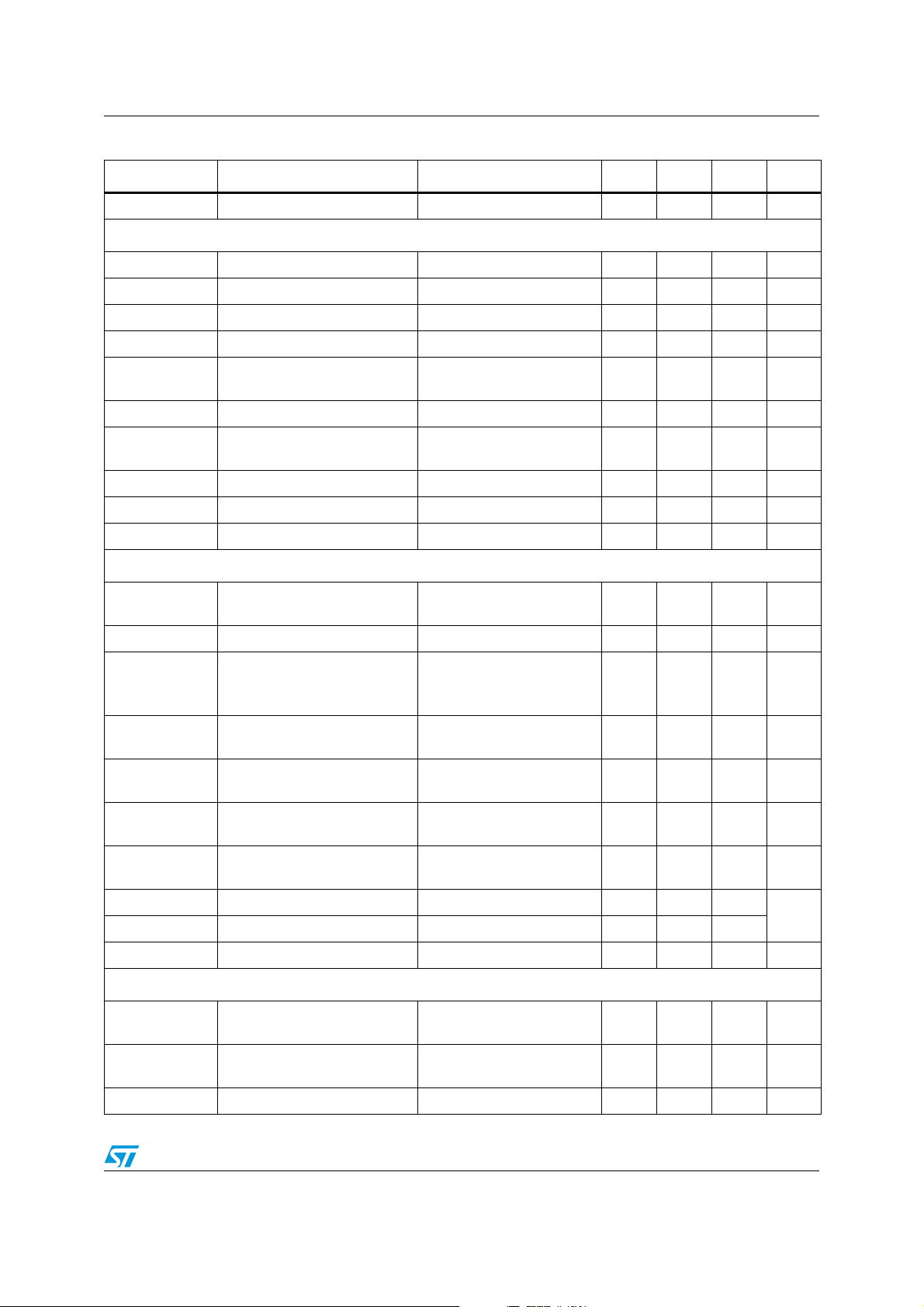
1 General description
1.1 Overview
L6460 offers the possibility to control and power multi motor systems, through the
management of simultaneous driving of stepper and DC motor. A number of features can be
configured through the digital interface (SPI), including 3 voltage regulators, 1 high precision
A/D converter, 2 operational amplifiers and 14 configurable GPIOs.
The high flexibility allows the possibility to configure two, one full or half bridge to work as
power stage featuring additional voltage buck regulators.
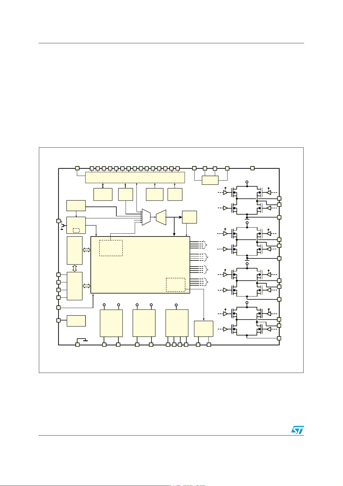
Figure 1. Block diagram
N2%3%4
N33
3#,+
-)3/
-/3)
N!7!+%
66
6'0)/?30)
4HERMAL
-ANAGER
3UPERVISORY
2ESET
-ANAGER
7$
2EGISTERS
30)
)NTERNAL
2EGULATOR
'0)/
/P!MP
'0)/
'0)/
X
S
3TEPPER-OTOR
-ANAGER
$#$#
-AIN
3WITCHING
2EGULATOR
'0)/
'0)/
'0)/
#URRENT
$!#
)NT6OLTAGE2EFERENCE
63UPPLY
'0)/
'0)/
'0)/
'0)/S
#ONTROL
,OGIC
60UMP60UMP
-AIN
,INEAR
2EGULATOR
'0)/
'0)/
'0)/
'0)/
07-
'ENERATORS
63UPPLY 63UPPLY
!$#-58
3WITCH
"ATTERY
#HARGER
-ANAGER
3WITCHING
2EGULATOR
#ONTROLLER
'0)/
X
'0)/
63UPPLY)NT
$IGITAL
#OMP
#0(
#HARGE
(3 $#X?-).53
,3 $#X?-).53
(3 $#X?0,53
,3 $#X?0,53
2EGOLATION
,OOP
$#
PUMP
#0,
60UMP
60UMP
60UMP
60UMP
60UMP
63UPPLY
63UPPLY
63UPPLY
63UPPLY
63UPPLY
60UMP
$#?-).53
$#?0,53
'.$
60UMP
$#?-).53
$#?0,53
'.$
60UMP
$#?-).53
$#?0,53
$#?3%.3%
60UMP
$#?-).53
$#?0,53
$#?3%.3%
%?0!$
)2%&?&"
62%&?&"
637MAIN?&"
637MAIN?37
Note: See following Chapter 2 for a detailed description of possible configurations.
6,).MAIN?/54
6,).MAIN?&"
637$26?3.3
637$26?&"
637$26?37
637$26?'!4%
10/139 Doc ID 17713 Rev 1

L6460 General description
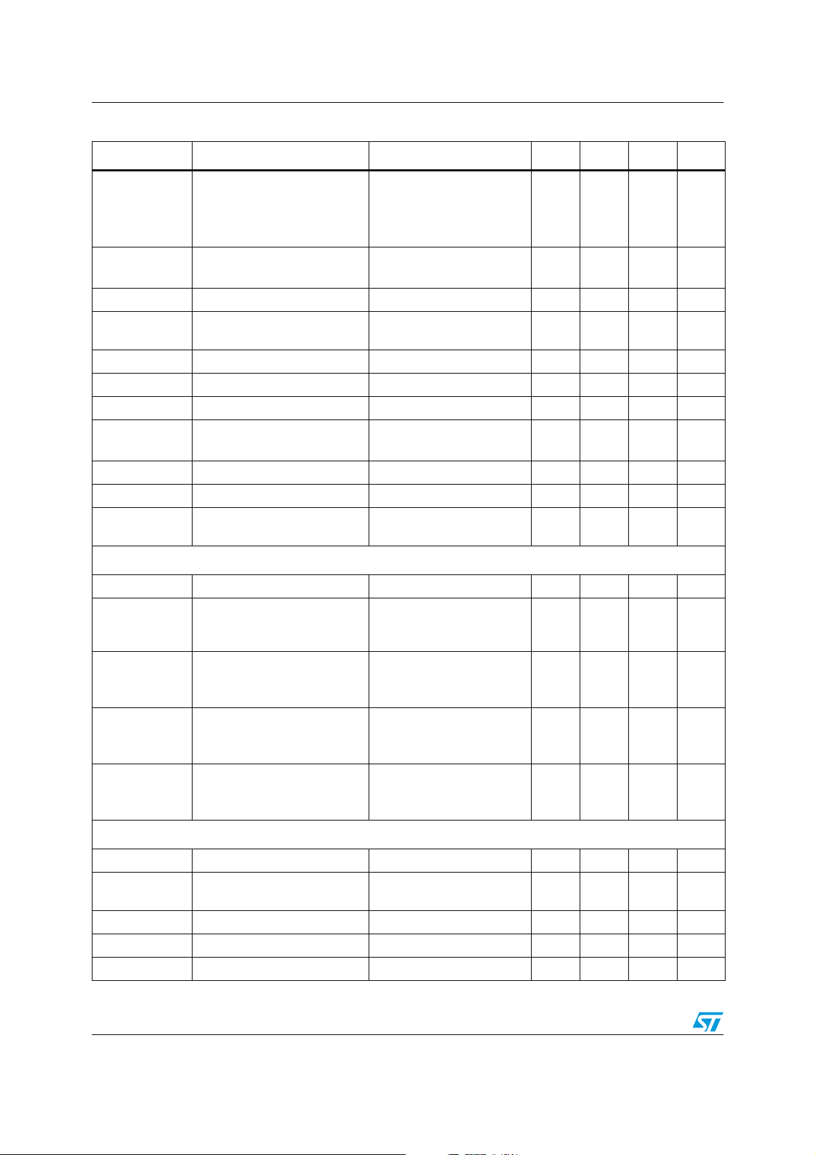
1.2 Pin connection
Figure 2. Pin connection
VSupply
DC1_PLUS
64 63 62 61 60 59 58 57
DC1_PLUS
V
SWDRV_SNS
VSWDRV_FB
DC1_MINUS
DC1_MINUS
DC2_MINUS
DC2_MINUS
DC2_PLUS
1
GND_PAD
2
3
4
GPIO4
5
GPIO3
6
7
8
GND1
GND2 DC4_SENSE
9 40
10
11
GPIO2
12
GPIO1
13
GPIO0
14
nSS
15
16
17 18 19 20 21 22 23 24
Supply
MISO
V
DC2_PLUS
CPL
CPH
MOSI
VPump
VLINmain_FB
VSWDRV_GATE
GPIO8
LINmain_OUT
VSWDRV_SW
GPIO6
56 55 54 53 52 51 50 49
25 26 27 28 29 30 31 32
Supply
V
SWmain_SW
V
VGPIO_SPI
GPIO7
SWmain_FB
V
VSupplyInt
REF_FB
V
V3V3
IREF_FB
nRESET
SCLK
VSupply
Supply
V
DC3_PLUS
N.C.
48
47
46
45
44
43
42
41
39
38
37
36
35
34
33
N.C.
DC4_PLUS
DC3_SENSE
GPIO5
GPIO9
GPIO10
GPIO11
N.C.
DC3_MINUS
DC3_SENSE
DC4_MINUS
N.C.
GPIO14
GPIO13
GPIO12
nAWAKE
DC4_SENSE
Doc ID 17713 Rev 1 11/139
General description L6460
1.3 Pin list
Table 2. Pins configuration
Pin # Pin name Description Type
1 DC1_PLUS Bridge 1 phase “plus” output Output
2V
3V
SWDRV_SNS
SWDRV_FB
4 GPIO4 General purpose I/O Analog In/Out - CMOS bi-dir
5 GPIO3 General purpose I/O Analog In/Out - CMOS bi-dir
6 DC1_MINUS Bridge 1 phase “minus” output Output
7 DC1_MINUS Bridge 1 phase “minus” output Output
8 GND1 Ground pin for bridge1
9 GND2 Ground pin for bridge2
10 DC2_MINUS Bridge 2 phase “minus” output Output
11 DC2_MINUS Bridge 2 phase “minus” output Output
12 GPIO2 General purpose I/O Analog In/Out - CMOS bi-dir
13 GPIO1 General purpose I/O Analog In/Out - CMOS bi-dir
Switching regulator controller sense Analog input
Switching regulator controller feedback Analog input
(1)(2)(3)
(1)(2)(3)
Power/digital
Power/digital
14 GPIO0 General purpose I/O Analog Input - CMOS input
15 nSS SPI chip select pin CMOS input
16 DC2_PLUS Bridge 2 phase “plus” output Output
17 DC2_PLUS Bridge 2 phase “plus” output Output
18 V
Supply
Main voltage supply Power input
19 MISO SPI serial data output CMOS output
20 MOSI SPI serial data input CMOS input
21 V
22 V
LINmain_FB
LINmain_OUT
Linear main regulator feedback Analog input
Linear main regulator output Power output
23 GPIO 8 General purpose I/O Analog In/Out - CMOS bi-dir
24 V
SWmain_SW
25 V
26 V
SWmain_FB
27 V
28 I
Supply
REF_FB
REF_FB
Main switching regulator switching output Power output
Main voltage supply Power Input
Main switching regulator feedback pin Analog input
Regulator voltage feedback Analog input
Regulator current feedback Analog input
29 SCLK SPI input clock pin CMOS input
30 V
31 DC4_PLUS Bridge 4 phase “plus” output Output
Supply
Main voltage supply Power input
32 N.C. Not connected
33 DC4_SENSE Bridge 4 sense output
(4)
34 nAWAKE Device wake up CMOS input
12/139 Doc ID 17713 Rev 1
Output
L6460 General description
Table 2. Pins configuration (continued)
Pin # Pin name Description Type
35 GPIO12 General purpose I/O Analog In/Out - CMOS bi-dir
36 GPIO13 General purpose I/O Analog In/Out - CMOS bi-dir
37 GPIO14 General purpose I/O Analog In/Out - CMOS bi-dir
38 N.C. Not connected
39 DC4_MINUS Bridge 4 phase “minus” output Output
40 DC4_SENSE Bridge 4 sense output
41 DC3_SENSE Bridge 3 sense output
(4)
(4)
42 DC3_MINUS Bridge 3 phase “minus” output Output
43 N.C. Not connected
44 GPIO11 General purpose I/O Analog In/Out - CMOS bi-dir
45 GPIO10 General purpose I/O Analog In/Out - CMOS bi-dir
46 GPIO9 General purpose I/O Analog In/Out - CMOS bi-dir
47 GPIO5 General purpose I/O Analog In/Out - CMOS bi-dir
(4)
48 DC3_SENSE Bridge 3 sense output
Output
49 N.C. Not connected
Output
Output
50 DC3_PLUS Bridge 3 phase “plus” output Output
51 V
Supply
Main voltage supply Power input
52 nRESET Open drain system reset pin CMOS Input/output
53 V
54 V
SupplyInt
3v3
Internal 3.3 volt regulator Power Input/output
Internal voltage supply Power Input
55 GPIO7 General purpose I/O Analog In/Out - CMOS bi-dir
56 V
GPIO_SPI
Low voltage pins power supply Power input
57 GPIO6 General purpose I/O Analog In/Out - CMOS bi-dir
58 V
59 V
SWDRV_SW
SWDRV_GATE
60 V
Pump
Switching regulator controller source input Power input
Switching driver gate drive pin Analog output
Charge pump voltage Power Input/output
61 CPH Charge pump high switch pin Power Input/output
62 CPL Charge pump low switch pin Power Input/output
63 V
Supply
Main voltage supply Power input
64 DC1_plus Bridge 1 phase “plus” output Output
E_Pad GND_PAD
1. These pins must be connected all together to a unique PCB ground.
2. Bridges1 and 2 have 2 ground pads: one is bonded to the relative ground pin (GND1 or GND2) and the
other is connected to exposed pad (E_Pad) ground ring. This makes the bond wires testing possible by
forcing a current between E-Pad and GND1 or GND2 pins and using the other pin as sense pin to measure
the resistance of E-Pad bonding. (N.B: grounds of two bridges are internally connected together).
3. The analog ground is connected to exposed pad E-Pad.
4. The pin must be tied to ground if bridge is not used as a stepper motor.
(1)(2)(3)
Doc ID 17713 Rev 1 13/139

L6460’s main features L6460
2 L6460’s main features
L6460 includes the following circuits:
● Four widely configurable full bridges:
– Bridges 1 and 2:
– Diagonal R
– Max operative current = 2.5 A.
– Bridges 3 and 4:
– Diagonal R
– Max operative current = 1.5 A.
● Possible configurations for each bridge are the following:
– Bridge 1:
– DC motor driver.
– Super DC (bridge 1 and 2 paralleled form superbridge1).
– 2 independent half bridges.
– 1 super half bridge (bridge 1 side A and bridge 1 side B paralleled form
superhalfbridge1).
– 2 independent switches (high or low side).
– 1 super switch (high or low side).
– Bridge 2 has the same configurations of bridge 1.
– Bridge 3 has the same configurations of bridge 1 (bridge 3 and 4 paralleled form
superbridge2) plus the following:
– ½ stepper motor driver.
– 2 buck regulators (V
– 1 Super buck regulator (V
– Bridge 4 has the same configurations of bridge 1 plus the following:
– ½ stepper motor driver.
– 1 super buck regulator (V
– Battery charger.
● One buck type switching regulator (V
– Output regulated voltage range: 1-5 Volts.
– Output load current: 3.0 A.
– Internal output power DMOS.
– Internal soft start sequence.
– Internal PWM generation.
– Switching frequency: ~250 kHz.
– Pulse skipping strategy control.
● One switching regulator controller (V
– Output regulated voltage range: 1-30 Volts.
– Selectable current limitation.
– Internal PWM generation.
– Pulse skipping strategy control.
● One linear regulator (V
14/139 Doc ID 17713 Rev 1
: 0.6 Ω typ.
DSon
: 0.85 Ω typ.
DSon
LINmain
AUX1_SW
AUX1//2_SW
AUX3_SW
, V
AUX2_SW
SWmain
SWDRV
).
).
).
) with:
) with:
) that can be used to generate low current/low ripple

L6460 L6460’s main features
voltages. This regulator can be used to drive an external bipolar pass transistor to
generate high current/low ripple output voltages.
● One bidirectional serial interface with address detection so that different ICs can share
the same data bus.
● Integrated power sequencing and supervisory functions with fault signaling through
serial interface and external reset pin.
● Fourteen general purpose I/Os that can be used to drive/read internal/external
analog/logic signals.
● One 8-bit/9-bit A/D converter (100 kS/s @ 9-bit, 200 kS/s @8-bit). It can be used to
measure most of the internal signals, of the input pins and a voltage proportional to IC
temperature.
– Current sink DAC:
– Three output current ranges: up to 0.64/6.4/64 mA.
– 64 (6-bit programmable) available current levels for each range.
– 5 V output tolerant.
● Two operational amplifiers:
– 3.3 V supply, rail to rail input compatibility, internally compensated.
– They can have all pins externally accessible or can be internally configured as a
buffer o make internal reference voltages available outside of the chip.
– Unity gain bandwidth > 1 MHz.
– They can also be set as comparators with 3.3 V input compatibility and low offset.
● Two 3.3 V pass switches with 1 Ω R
● Programmable watchdog function.
● Thermal shutdown protection with thermal warning capability.
● Very low power dissipation in “low power mode” (~35 mW)
and short circuit protected.
DSon
L6460 is intended to maximize the use of its components, so when an internal circuit is not
used it could be employed for other applications. Bridge 3, for example, can be used as a full
bridge or to implement two switching regulators with synchronous rectification: to obtain this
flexibility L6460 includes 2 separate regulation loops for these regulators; when the bridge is
used as a motor driver, the 2 regulation loops can be redirected on general purpose I/Os to
leave the possibility to assembly a switching regulator by only adding an external FET.
Doc ID 17713 Rev 1 15/139

Electrical specifications L6460
3 Electrical specifications
3.1 Absolute maximum rating
The following specifications define the maximum range of voltages or currents for L6460.
Stresses above these absolute maximum specifications may cause permanent damage to
the device. Exposure to absolute maximum ratings for extended periods may affect device
reliability.
Table 3. Absolute maximum ratings
Parameter Description
V
V
Supply
V
GPIO_SPI
V
3V3pin
V
SW
V
SW_pulse
V
Pump
T
J
1. This value is useful to define the voltage rating for external capacitor to be connected from V
V
. V
Supply
to provide voltage to external loads.
2. TSD is the thermal shut down temperature of the device.
is internally generated and can never be supplied by external voltage source nor is intended
Pump
voltage 40 V
Supply
V
GPIO_SPI
V
3V3
voltage 3.9 V
voltage -0.3 3.9 V
Switching regulators output pin voltage
range
Switching regulators min pulsed
voltage
Charge pump voltage
Junction temperature
3.2 Operating ratings specifications
Table 4. IC operating ratings
Parameter Description
V
V
Supply
I
Supply
I
Shut_down
V
GPIO_SPI
I
VGPIO_SPI
V
3v3
V
LINmain_OUT
V
LINmain_FB
V
SWmain_SW
V
SWDRV_SWVSWDRV_SW
voltage range 13
Supply
V
operative current
Supply
V
shut down state current 1.5 mA
Supply
V
GPIO_SPI
V
GPIO_SPI
voltage range 2.4 3.6 V
operative current
3.3V input pin voltage range 3.6 V
Output pin voltage range
Feedback pin voltage range 0 3.6 V
Output pin voltage range
pin voltage range
(2)
Test
condition
tpulse <
500ns
(1)
Min Max Unit
-1 V
Supply
-3 V
15 V
Storage -40 190 °C
Operating -40 TSD °C
to
Pump
Tes t
condition
(2)
(3)
(4)
(4)
(4)
-1 V
Min Max Unit
(1)
38 V
15 mA
0.4 mA
0V
Supply
-1 V
supply
Supply
V
V
V
V
16/139 Doc ID 17713 Rev 1
L6460 Electrical specifications
Table 4. IC operating ratings
Parameter Description
Tes t
condition
Min Max Unit
V
SWDRV_GATE
V
SWDRV_SNS
T
J
1. For V
2. Operating supply current is measured with system regulators operating but not loaded.
3. Operating V
4. The external components connected to the pin must be chosen to avoid that the voltage exceeds this
supply
For V
supply
amplifiers and pass switches) enabled but not loaded.
operative range.
Gate drive pin voltage 0 V
V
Sense pin voltage
Supply
-3V
V
Junction temperature Operating -40 125 °C
lower than 21 V an external resistor between V
lower than 15 V external diodes for charge pump are required.
current is measured with all circuits supplied by V
GPIO_SPI
supply
and V
supply Int
GPIO_SPI
pins are required.
(GPIO’s, operational
Pump
Supply
3.3 Electrical characteristics
Table 5. Electrical characteristics
Parameter Description Test condition Min Typ Max Unit
V
SupplyInt
Charge pump V
V
I
S_Int
V
F
Pump
S_Int
Pump
regulator
Pump
V
SupplyInt
V
SupplyInt
output voltage
operative current
Charge pump voltage V
V
clock frequency F
Pump
(1)
(2)
Supply
= 16MHz typ
OSC
=32V
18 19.5 21 V
11 mA
Supply
V
Supply
+12.5
F
OSC
/6
V
Supply
+ 14.5
V
+ 10.5
4
V
V
V
kHz
V3V3 regulator
Power on reset
V
V
nRESET circuit
V
3V3
Supply_POR_validVSupply
Supply_POR_fallVSupply
t
Supply_POR_filtVSupply
V
3V3_POR_fallV3v3
V
3V3_POR_riseV3v3
V
3V3_POR_hysV3v3
t
3V3_POR_filt
V
nRST_L
V
output voltage V
3v3
POR falling threshold V
POR rising threshold V
POR hysteresis 0.5 V
V
POR filter time 1.5 µs
3v3
nRESET low level output
voltage
=32V 3.15 3.3 3.45 V
Supply
voltage for POR valid I
POR falling threshold V
= 1mA 4 V
nRESET
falling 6 8 V
Supply
POR filter Time 3 µs
falling 1.9 2.2 V
3V3
rising 2.7 V
3V3
I=10mA 0.4 V
Doc ID 17713 Rev 1 17/139
Electrical specifications L6460
Table 5. Electrical characteristics (continued)
Parameter Description Test condition Min Typ Max Unit
t
nRST_fall
t
nRST_del
V
Supply_UV_f
V
Supply_UV_r
V
Supply_UV_hysVSupply
t
Supply_UV
V
S_Int_UV_f
V
S_Int_UV_r
V
S_Int_UV_hysVSupplyInt
t
S_Int_UV
V
Pump_UV_f
V
Pump_UV_r
V
Pump_UV_hysVPump
t
Pump_UV
V
GPIO_SPI_UV_fVGPIO_SPI
V
GPIO_SPI_UV_rVGPIO_SPI
V
GPIO_SPI_hysVGPIO_SPI
t
GPIO_SPI_UV
nRESET fall time
nRESET delay time
V
Supply
V
Supply
V
Supply
V
SupplyInt
V
SupplyInt
V
SupplyInt
V
Pump
V
Pump
V
Pump
V
GPIO_SPI
TSD circuit
I=1mA
C=50pF
(4)
(3)
15 ns
150 ns
falling threshold 10.2 11 11.8 V
rising threshold 10.5 11.5 12.5 V
hysteresis 0.3 0.5 0.7 V
UV filter time 3.5 µs
falling threshold 9.7 10.7 11.7 V
rising threshold 10.6 11.4 12.2 V
hysteresis 0.4 0.7 1 V
UV filter time 3.5 µs
V
V
falling threshold
rising threshold
V
Supply
+7
V
Supply
+ 7.5
Supply
+ 7.5
V
Supply
+ 8
Supply
+ 8
V
Supply
+ 8.5
hysteresis 0.3 0.5 0.7 V
UV filter time 3.5 µs
falling threshold 1.8 2 V
rising threshold 2.2 2.4 V
hysteresis 200 250 300 mV
UV filter time 3.5 µs
V
V
T
TSD
T
WARM
T
DIFF
t
TSD_FILT
t
WARM_F ILT
Thermal shut down
temperature
Warming temperature 140 °C
Thermal shut down to warming
difference
Thermal shut down filter time 8 µs
Warming filter time 8 µs
Watchdog
WD_T
clk
Watchdog clock period
Internal clock
F
osc
Oscillator frequency V
3V3
nAWAKE function
V
IL
nAWAKE low logic level
voltage
18/139 Doc ID 17713 Rev 1
170 °C
30 °C
*
T
osc
2
22
s
= 3.3 V 14.1 16 17.6 MHz
0.8 V
L6460 Electrical specifications
Table 5. Electrical characteristics (continued)
Parameter Description Test condition Min Typ Max Unit
V
IH
V
HYS
I
OUT
I
INP
t
AWAKEFILT
nAWAKE high logic level
voltage
nAWAKE input hysteresis 0.25 V
nAWAKE pin output current nAWAKE=0V
nAWAKE pin input current nAWAKE=0.8V
Filter time 1.2 μs
Main linear regulator
V
drop
I
PD
V
LINmain_Ref
I
LINmain_Ref
I
outLINMax
I
short
ΔV
out/Vo
/ΔV
ΔV
out
V
loop_acc
V
LIN_UV_f
V
LIN_UV_r
V
LIN_UV_hys
t
prim_uv
Supply
Drop out voltage
Internal switch pull down
current
Feedback reference voltage 0.776 0.8 0.824 V
Feedback pin input current -2 2 µA
Maximum output current V
Output short
circuit current
Load regulation 0 ≤ I
Line regulation I
Loop voltage accuracy ±2.5 %
Undervoltage falling threshold
Undervoltage rising threshold
Undervoltage hysteresis 6 %
Under voltage deglitch filter 5 µs
Main switching regulator
(5)
(5)
=
V
drop
V
supply-VLINmain_OUT
Linear Main Regulator
disabled; V
LINmain_OUT
V
LINmain_OUT
V
LINmain_FB
load
(7)
(7)
≤ I
load
=10mA
LINmain_OUT
= V
supply
=0V,
=0V
outLINMax
(6)
(6)
1.6 V
-0.72 -2 mA
0.2 0.4 mA
2V
=1V
3mA
-2V 10 mA
12 24 32 mA
0.8 %
0.2 %
84.5 87 89.5 %
90.5 93 95.5 %
SelFBref = ‘00’ 0.776 0.8 0.824 V
(8)
0.97 1 1.03 V
V
FBREF
Main switching regulator
feedback reference voltage
SelFBref = ‘01’
SelFBref = ‘10’ 2.425 2.5 2.575 V
SelFBref = ‘11’ 2.91 3 3.09 V
I
Q
I
Q_LP
I
SWmain_FB
V
SWmain_OUT
I
load
R
DSonHS
Output leakage current T
Output leakage current in
“low power mode”
V
SWmain_FB
pin current T
Output voltage range
Maximum output load current V
Internal high side R
DSon
= 125°C -40 +40 µA
junction
V
= 36V
Supply
= 125°C
T
junction
= 125°C -10 +10 µA
junction
(9)
= 36V 0.002 3 A
Supply
I
=1A
load
= 125°C
T
junction
-15 +15 µA
0.8 5 V
0.33 0.95 Ω
Doc ID 17713 Rev 1 19/139
Electrical specifications L6460
Table 5. Electrical characteristics (continued)
Parameter Description Test condition Min Typ Max Unit
V
loop
V
SW_UV_f
V
SW_UV_r
V
SW_UV_hys
t
prim_uv
I
limit
t
deglitch
t
I_lim
t
I_limUV
t
r
t
f
F
SW_PWM
Loop voltage accuracy ±3%
Under voltage falling threshold
Under voltage rising threshold
Under voltage hysteresis 6 %
Under voltage deglitch filter 5 µs
Current limit protection
Current limit deglitch time 50 ns
Current limit response time
Current limit response time in
UV condition
Switching output rise time
Switching output fall time
Operating frequency
Switching regulator controller
(10)
(10)
SelIlimit =”0”
SelIlimit =”1”
Normal operating mode (no
(11)
UV)
UV condition
V
= 36V,
Supply
= 422 Ω
R
LOAD
V
= 36V,
Supply
= 10 Ω
R
LOAD
(12)
200 400 ns
(13)
(13)
84.5 87 89.5 %
90.5 93 95.5 %
3.3
2.3
5
3.5
A
A
450 650 ns
530ns
530ns
Fosc/6
4
kHz
V
GS_ext
I
SOURCE
I
SINK
t
SINK
R
SUSTAIN
I
Q
I
Q_LP
V
FBREF
I
SWDRV_FB
V
loop
Gate to source voltage for
external FET
Source current
Sink current V
V
Pump=VSupply
V
SWCTR_GATE
SWCTR_GATE
+12V
=0V
= V
Supply
V
Pump
25 50 mA
20 mA
Sink discharge pulse time 600 ns
Gate-source sustain
resistance
Output
leakage current
Output leakage current in
“Low Power Mode”
Switching regulator feedback
(V
SWCTR_GATE
V
SWCTR_SRC
= 36V,
V
Supply
T
junction
V
= 36V,
Supply
T
junction
SelFBref = ‘00’
) = 0.2V
= 125°C
= 125°C
-
(8)
650 Ω
-40 +40 µA
-5 +5 µA
0.776 0.8 0.824 V
SelFBref = ‘01’ 0.97 1 1.03 V
controller feedback reference
voltage
SelFBref = ‘10’ 2.425 2.5 2.575 V
SelFBref = ‘11’ 2.91 3 3.09 V
V
SWDRV_FB
pin current
Supply
T
junction
= 125°C
-10 +10 µA
V
= 36V,
Loop voltage accuracy ±3%
V
20/139 Doc ID 17713 Rev 1
L6460 Electrical specifications
Table 5. Electrical characteristics (continued)
Parameter Description Test condition Min Typ Max Unit
V
SWD_UV_f
V
SWD_UV_r
V
SWD_UV_hys
t
prim_uv
V
ovc
t
deglitch
t
I_lim
t
I_limUV
Under voltage falling threshold
Under voltage rising threshold
Under voltage hysteresis 6 %
Under voltage deglitch filter 5 µs
Over current threshold voltage 250 300 350 mV
Current limit deglitch time 50 ns
Current limit response time
Current Limit response time in
UV condition.
(14)
(14)
Normal operating mode (no
(11)
UV)
UV condition
(12)
84.5 87 89.5 %
90.5 93 95.5 %
500 900 ns
380 550 ns
F
SWD_PWM
Power bridges
R
DSon1_2
R
DSon3_4
I
MAX1_2
I
MAX3_4
I
dss
I
Q_LP
I
OC_LS1_2
I
OC_HS1_2
Operating frequency F
Bridge 1 and 2 diagonal R
Bridge 3 and 4 diagonal R
DSon
DSon
I = 1.4A, V
= 125°C
T
junction
I = 1A, V
= 125°C
T
junction
Supply
Supply
= 36V,
= 36V,
Bridge 1 and 2 operative rms
current
Bridge 3 and 4 operative rms
current
Output leakage current. T
Output leakage current in “low
power mode”
Low side current protection for
bridges 1 and 2
High side current protection for
bridges 1 and 2
(15)
(15)
= 125°C -50 +50 µA
junction
V
= 36V,
Supply
T
= 125°C
junction
MtrXSideYILimSel[1:0]=00
MtrXSideYILimSel[1:0]=01
MtrXSideYILimSel[1:0]=10
MtrXSideYILimSel[1:0]=11
(16)
MtrXSideYILimSel[1:0]=00
MtrXSideYILimSel[1:0]=01
MtrXSideYILimSel[1:0]=10
MtrXSideYILimSel[1:0]=11
6)
-10 +10 µA
0.6
1.4
2.4
2.4
0.7
1.5
2.5
(1
2.5
/64 kHz
osc
0.6 1.1
0.85 1.65
2.5 A
1.5 A
1
2
3
3
1
2
3
3
1.6
2.6
3.6
3.6
1.7
2.7
3.7
3.7
Ω
Ω
A
A
I
OC_LS3_4
I
OC_HS3_4
t
filter
Low side current protection for
bridges 3 and 4
High side current protection for
bridges 3 and 4
(15)
(15)
Current limit
filter time
MtrXSideYILimSel[1:0]=11
(17)(18)
MtrXSideYILimSel[1:0]=11
7)(18)
1.55 2.5 A
(1
1.6 2.5 A
25μs
Doc ID 17713 Rev 1 21/139
Electrical specifications L6460
Table 5. Electrical characteristics (continued)
Parameter Description Test condition Min Typ Max Unit
t
delay
t
OC_off
t
r1_2
t
r3_4
t
f1_2
t
f3_4
t
deadRise
t
deadFall
F
PWM
Current limit
delay time
Over current Off time
Output rise time
bridges 1 and 2
Output rise time
bridges 3 and 4
Output fall time
bridges 1 and 2
Output fall time
bridges 3 and 4
MtrXIlimitOffTimeY[1:0]=00
MtrXIlimitOffTimeY[1:0]=01
MtrXIlimitOffTimeY[1:0]=10
MtrXIlimitOffTimeY[1:0]=11
(19)
V
= 36V, resistive load
Supply
between outputs:
R= 25 Ω
V
between outputs:
R= 36 Ω
V
(20)
= 36V, resistive load
Supply
(20)
= 36V, resistive load
Supply
between outputs:
R= 25 Ω
V
(20)
= 36V, resistive load
Supply
between outputs:
R= 36 Ω
(20)
100 180 250 ns
50 100 200 ns
100 180 250 ns
50 125 250 ns
5 μs
60
120
240
480
µs
µs
µs
µs
Anti crossover rising dead time 100 300 450 ns
Anti crossover falling dead
time
Operating frequency
100 300 450 ns
/51
F
osc
2
kHz
t
resp
Delay from PWM to output
transition
Bipolar stepper circuitry
V
STEPREF
V
offset
Reference voltage
Sense comparator offset -12 12 mV
SelStepRef =0
SelStepRef =1
StepBlkTime = ‘00’
StepBlkTime = ‘01’ 1 1.45 1.9 µs
t
blk
Blanking time
StepBlkTime = ‘10’ 1.5 2.25 3 µs
StepBlkTime = ‘11’ 3 4.25 5.5 µs
Synchronous buck regulator (bridge 3)
V
AUX_SW
I
Q
I
QLP
Output pin voltage range
(DC3x)
Output leakage current T
Output leakage current in “Low
Power Mode”
(26)
junction
V
Supply
T
junction
22/139 Doc ID 17713 Rev 1
500 ns
(8)
0.48
0.72
0.65 0.95 1.25 µs
-1 V
0.50
0.75
0.52
0.78
Supply
= 125°C -50 +50 µA
= 36V
= 125°C
-10 +10 µA
V
V
L6460 Electrical specifications
Table 5. Electrical characteristics (continued)
Parameter Description Test condition Min Typ Max Unit
SelFBRef = ‘00’ 0.776 0.8 0.824 V
(21)
(22)
0.97 1 1.03 V
2.425 2.5 2.575 V
-15 15 µA
(23)
0.8 30 V
=1A 0.6 0.8 Ω
load
84.5 87 89.5 %
90.5 93 95.5 %
480 700 ns
V
FBREF
I
GPIO_FB
V
out
I
load
R
DSonHS
V
loop
V
REG_UV_f
V
REG_UV_r
V
REG_UV_hys
t
aux_UV
I
limit
t
deglitch
t
I_lim
Synchronous buck regulator
feedback reference voltage
SelFBRef = ‘01’
SelFBRef = ‘10’
SelFBRef = ‘11’ 2.91 3 3.09 V
T
= 125°C
GPIO feedback pin current
Output voltage range V
Output load current V
Internal high/low side R
DSon
junction
0V≤Feedback ≤ 3V
= 36V
Supply
= 36V 0.002 1.5 A
Supply
T
= 125°C; I
junction
Loop voltage accuracy ±3%
Under voltage falling threshold
Under voltage rising threshold
(24)
(24)
Under voltage hysteresis 6 %
Under voltage deglitch filter 5 µs
Current limit protection 1.6 2.5 A
Current limit deglitch time 50 ns
Current limit response time
Normal operating mode
(no UV)
(11)
t
I_limUV
t
r
t
f
t
dead
F
REGPWM
Battery charger (Bridge 4)
V
AUX3_SW
I
Q
V
FBRef
Current limit response time in
UV condition.
Switching output rise time
Switching output fall time
UV condition
V
Supply
R
LOAD
V
Supply
R
LOAD
(12)
= 36V,
= 422 Ω
= 36V,
= 10 Ω
(25)
(23)
350 500 ns
530ns
10 50 ns
Crossover dead time 100 ns
Operating frequency F
Output pin voltage range
(DC4x)
Output leakage current T
(26)
-1 V
= 125°C -100 +100 µA
junction
/64 kHz
osc
Supply
SelFBRef = ‘00’ 1.37 1.412 1.455 V
Battery charger control loop
feedback reference voltage
SelFBRef = ‘01’
(8)
SelFBRef = ‘10’ 2.079 2.143 2.207 V
1.746 1.8 1.854 V
SelFBRef = ‘11’ 2.425 2.5 2.575 V
V
Doc ID 17713 Rev 1 23/139
Electrical specifications L6460
Table 5. Electrical characteristics (continued)
Parameter Description Test condition Min Typ Max Unit
SelCurrRef = ‘00’
(8)
0.873 0.9 0.927 V
V
CurrRef
V
out
I
load
R
DSon
V
loop
V
BC_UV_f
V
BC_UV_r
V
BC_UV_hys
t
aux_UV
I
limit
t
deglitch
t
I_lim
t
I_limUV
t
r
t
f
t
dead
F
BCPWM
Battery charger control loop
feedback reference current
Output voltage range V
Output load current V
Internal high/low side R
Loop voltage accuracy ±3%
Under voltage falling threshold
Under voltage rising threshold
Under voltage hysteresis 6 %
Under voltage deglitch filter 5 µs
Current limit protection 3.2 5 A
Current limit deglitch time 50 ns
Current limit response time
Current limit response time in
UV condition.
Switching output rise time
Switching output fall time
Crossover dead time 100 ns
Operating frequency F
ADC with A2DType=0
(29)
DSon
SelCurrRef = ‘01’ 1.394 1.437 1.48 V
SelCurrRef = ‘10’ 1.746 1.8 1.854 V
SelCurrRef = ‘11’ 2.182 2.25 2.318 V
(27)
= 36V
Supply
= 36V 0.002 3 A
Supply
T
= 125°C;
junction
= 1.5A
I
LOAD
(28)
(28)
Normal operating mode
(no UV)
UV condition
V
R
V
R
Supply
LOAD
Supply
LOAD
(11)
(12)
= 36V,
= 422 Ω
= 36V,
= 10 Ω
(25)
(25)
1.412 30 V
0.3 0.4 Ω
84.5 87 89.5 %
90.5 93 95.5 %
480 700 ns
350 500 ns
530ns
10 50 ns
/64 kHz
osc
IMR Measurement range A2dType = 0 0 V
INL Integral non-linearity A2dType = 0
DNL Differential non-linearity A2dType = 0
OE Offset error A2dType = 0
OE
Drift
Offset error drift
A2dType = 0 over time
and temperature
GE Gain error A2dType = 0
GE
t
Drift
conv
Gain error drift
Minimum conversion time 55 µs
Resolution
A2dType = 0 over time
and temperature
(35)
24/139 Doc ID 17713 Rev 1
V
(30)(31)
(32)(31)
(33)
3v3
±2 LSB
±2 LSB
±4 LSB
±3 LSB
(34)
±4 LSB
±4 LSB
8bits
L6460 Electrical specifications
Table 5. Electrical characteristics (continued)
Parameter Description Test condition Min Typ Max Unit
C
in
Input sampling capacitance
ADC with A2DType=1
(37)
(36)
4pF
IMR Measurement range A2dType = 1 0 V
INL Integral non-linearity A2dType = 1
DNL Differential Non-Linearity A2dType = 1
OE Offset error A2dType = 1
OE
Drift
Offset error drift
A2dType = 1 over time and
temperature
GE Gain error A2dType = 1
GE
t
Drift
conv
Gain error drift
Minimum conversion time 10 µs
A2dType = 1
over time and temperature
(30)(31)
(32)(31)
(33)
(34)
Resolution 9 bits
C
in
Input sampling capacitance
(36)
Current DAC
V
R
I
OUT_OFF
I
FULL_ERR
INL
10_11
DNL
10_11
Pin voltage operative range
(GPIO8)
Output off leakage current DacValue[5:0] = 000000 -1 +1 µA
Full scale current error
Integral non-linearity for 10
and 11 ranges
Differential non-linearity for 10
and 11 ranges
(38)
DacRange[1:0] =xx
DacValue[5:0] = 111111
0.7 5.5 V
-15 +15
3v3
V
±1 LSB
±1 LSB
±4 LSB
±3 LSB
±4 LSB
±4 LSB
4pF
% of
I
FULL
typ
±2 LSB
±2 LSB
INL
DNL
R
CurrDac_res
R
CurrDac_ratio
t
set
Operational amplifier
V
GPIO_SPI
V
ICM
V
OUT_MAX
01
01
Integral non-linearity for 01
range
Differential non-linearity for 01
range
Gpio[8] divider total resistance 45
Gpio[8] divider ratio 3/5
Settling time
(40)
Operational amplifier supply
voltage range
Input common mode voltage
range
Output voltage I
(39)
3.15 3.3 3.45 V
0
=± 1mA 0.1 3.2 V
LOAD
Doc ID 17713 Rev 1 25/139
±1 LSB
±1 LSB
kΩ
5µs
V
GPIO_
SPI
V
Electrical specifications L6460
Table 5. Electrical characteristics (continued)
Parameter Description Test condition Min Typ Max Unit
VOp1PlusRef
VOp2PlusRef
Operational amplifier 1 and 2
reference voltage
Avd Open loop gain
OpxRef[1:0]=00
OpxRef[1:0]=01
OpxRef[1:0]=10
OpxRef[1:0]=11
=1.65V
V
ICM
I
= 0mA
LOAD
0.97
1.6
1.94
2.425
90 dB
1
1.65
2
2.5
1.03
2.06
2.575
CMRR Common mode rejection ratio 80 110 dB
I
= ±6mA
(40) (41)
LOAD
V
=1.65V
ICM
C
=100pF V
load
=330 Ω to V
R
load
=1.65V 10 mA
out
I
= 0
load
C
=100pF
LOAD
=1.65V
ICM
GPIO_SPI
2MHz
1.3 1.75 V/µs
90 dB
PSRR Power supply rejection ratio
I
in _offs
I
in _bias
V
in _offs
Input offset current -150 150 nA
Input bias current -500 500 nA
Input offset voltage -5 5 mV
GBWP Gain bandwidth product
I
out
I
short_max
Output current V
Short circuit current 12 20 mA
SR Slew rate
Operational amplifier used as comparator
1.7
V
V
Low power switch
V
OUT_MAX
t
OFF
t
FAL L
t
ON
t
RISE
V
PSW
OUT_MAX
R
DSon
I
LIMIT
t
deglitch
Output voltage I
=± 10mA 0.3 2.9 V
load
VCM = 1.65V
Turn off propagation delay
Fall time
Turn on propagation delay
Rise time
Δ Vi = -/+ 20mV
C
=100pF
LOAD
= 1.65V
V
CM
Δ Vi = -/+ 20mV
=100pF
C
LOAD
= 1.65V
V
CM
Δ Vi = -/+ 20mV
=100pF
C
LOAD
= 1.65V
V
CM
Δ Vi = -/+ 20mV
=100pF
C
LOAD
(42)(43)
(42)(43)
(42)(43)
(42)(43)
0.6 1 µs
0.15 0.4 µs
0.25 0.5 µs
0.2 0.4 µs
Input voltage range 2.4 3.6 V
V
Output voltage
Switch R
DSon
resistance I
=100mA 0.6 1 Ω
load
GPIO_
SPI
V
Current limit 150 250 350 mA
Current limit deglitch time 50 ns
26/139 Doc ID 17713 Rev 1
L6460 Electrical specifications
Table 5. Electrical characteristics (continued)
Parameter Description Test condition Min Typ Max Unit
t
I_lim
C
LOAD
t
t
OFF
ON
Current limit response time 650 ns
Max load capacitance 2.5 µF
V
Turn on propagation delay
Turn off propagation delay
GPIO_SPI
C
LOAD
V
GPIO_SPI
I
LOAD
C
LOAD
Interrupt controller
t
PULSE
t
INTFILT
Pulse duration 16*T
Filter time 200 ns
GPIO[0], GPIO[1], GPIO[2], GPIO[3], GPIO[4], GPIO[6]
V
IH
V
IL
V
HYS
V
OL
I
LEAKAGE
t
DELAY
High level input voltage 1.6 V
Low level input voltage 0.8 V
Input voltage hysteresis 0.15 0.22 V
Low level output voltage I
= 15mA 0.5 V
OUT
Leakage current 0 ≤ V
Delay from serial write to pin
Low
C
LOAD
=100pF
=1mA
=100pF
≤ V
out
=50 pF
=3.3V I
(44)
=3.3V
(44)
3v3
(45)
LOAD
=1mA
450 650 ns
250 450 ns
osc
µs
-1 1 µA
500 ns
GPIO[5], GPIO[7], GPIO[9], GPIO[10], GPIO[11], GPIO[12], GPIO[13], GPIO[14]
V
IH
V
IL
V
HYS
V
OL
V
OH
I
LEAKAGE
t
DELAY
High level input voltage 1.6 V
Low level input voltage 0.8 V
Input voltage hysteresis 0.15 0.22 V
Low level output voltage I
High level output voltage I
Leakage current 0 ≤V
Delay from serial write to pin
low
= 15mA 0.5 V
OUT
= 5mA 2.75 V
OUT
≤ V
out
3v3
C
LOAD
=50 pF
(45)
GPIO[8]
V
IH
V
IL
V
HYS
V
OL
I
LEAK_0
I
LEAK_1
High level input voltage 1.6 V
Low level input voltage 0.8 V
Input voltage hysteresis 0.13 0.22 V
Low level output voltage I
Leakage current
Leakage current
= 15mA, 0.4 V
OUT
EnGpio8DigIn=0,
0 ≤ Vout ≤ 5V
EnGpio8DigIn=1,
0 ≤ Vout ≤ 5V
-1 1 µA
500 ns
-1 1 µA
-1 5 µA
Doc ID 17713 Rev 1 27/139
Electrical specifications L6460
Table 5. Electrical characteristics (continued)
Parameter Description Test condition Min Typ Max Unit
ADChannelX[4:0]
I
AD
t
DELAY
SPI interface
V
IH
V
IL
V
HYS
V
OH
V
OL
t
SCLK
t
SCLK_rise
t
SCLK_fall
t
SCLK_high
t
SCLK_low
t
nSS_setup
t
nSS_hold
t
nSS_min
t
MOSI_setup
t
MOSI_hold
t
MISO_rise
t
MISO_fall
t
MISO_valid
t
MISO_disable
C
LOAD
1. This value is useful to define the voltage rating for external capacitor to be connected from V
2. This typical value is only intended to give an estimation of the current consumption when L6460 is configured in simple
regulators mode (see following Chapter 8.6.4) at the end of the start up sequence and with no load on regulators. This
typical value allows a raw choose of the external resistor but the definitive choose must be done according to the
recommendations on Chapter 4.1).
3. Measured between 10% and 90% of output voltage transition.
4. Measured from a fault detection to 50% of output voltage transition.
5. Current is defined to be positive when flowing into the pin.
6. Load regulation is calculated at a fixed junction temperature using short load pulses covering all the load current range. This
is to avoid change on output voltage due to heating effect.
7. Undervoltage rising and falling thresholds are intended as a percentage of feedback pin voltage (V
8. Default state.
9. The regulated voltage can be calculated using the formula: V
A/D path absorbed current
=10001 and
-1 1 µA
bit EnDacScale=0
Delay from serial write to pin
low
(40)
High level input voltage
Low level input voltage
Input voltage hysteresis
High level output voltage I
Low level output voltage I
C
(46)
(46)
(46)
OUT
OUT
LOAD
=50 pF
= -10mA,
= 10mA,
(45)
500 ns
1.6 V
0.8 V
0.15 0.22 V
(47)
(47)
2.75 V
0.4 V
SCLK period 62.5 ns
SCLK rise time 2 ns
SCLK fall time 2 ns
SCLK high time 20 ns
SCLK low time 20 ns
nSS setup time 10 ns
nSS hold time 10 ns
nSS high minimum time 30 ns
MOSI setup time 10 ns
MOSI hold time 10 ns
MISO rise time C
MISO fall time C
LOAD
LOAD
=50pF
=50pF
(48)
(48)
9ns
9ns
MISO valid from clock low 0 15 ns
MISO disable time 0 15 ns
MOSI maximum load 200 pF
SWmain_OUT = VFBREF
Supply
*(Ra+Rb)/Rb.
to V
LINmain_FB
SupplyInt
.
).
28/139 Doc ID 17713 Rev 1

L6460 Electrical specifications
10. Undervoltage rising and falling thresholds are intended as a percentage of feedback pin voltage (V
SW_main_FB
11. This condition is intended to simulate an extra current on output.
12. This condition is intended to simulate a short circuit on output.
13. Rise and fall time are measured between 10% and 90% V
14. Undervoltage rising and falling thresholds are intended as a percentage of feedback pin voltage (V
SWmain
output voltage.
SWDRV_FB
15. The current protection values must be intended as a protection for the chip and not as a continuous current limitation. The
protection is performed by switching off the output bridge when current reaches values higher than the I
protection could be guaranteed for values in the middle range between I
MAX
and I
OC
max. No
OC
16. In this cell X stands for 1 or 2, Y stands for A or B
17. In this cell X stands for 3 or 4, Y stands for A or B
18. The current protection thresholds for Bridge 3 and 4 are not selectable so only the max current value
(MtrXSideYILimSel[1:0]= 11) is available.
19. Overcurrent Off time can be configured using SPI.
20. Rise and fall time are measured between 10% and 90% of DC output voltage. With device in full bridge configuration
(resistive load between outputs).
21. Default state for Aux1
22. Default state for Aux2
23. The regulated voltage can be calculated using the formula: V
AUX_SW
= V
FBREF
*(Ra+Rb)/Rb.
24. Undervoltage rising and falling thresholds are intended as a percentage of feedback pin voltage (GPIO1 and/or GPIO2)
25. Rise and fall time is measured between 10% and 90% of output voltage.
26. The external components connected to the pin must be chosen to avoid that the voltage exceeds this operative range.
27. The regulated voltage can be calculated using the formula: V
AUX3_SW
= V
28. Undervoltage rising and falling thresholds are intended as a percentage of feedback pin voltage (V
7.5
29. The definition of LSB for this table is LSB=IMRmax/(2
30. Integral Non Linearity error (INL) is defined as the maximum distance between any point of the ADC characteristic and the
“best straight line” approximating the ADC transfer curve.
-1).
FBREF
*(Ra+Rb)/Rb.
REF_FB
).
31. The ADC ensures monotonic characteristic and no missing codes.
32. Differential nonlinearity error (DNL) is defined as the difference between an actual step width and the ideal width value of 1
LSB.
33. Offset error (OE) is the deviation of the first code transition (000...000 to 000...001) from the ideal (i.e. GND + 0.5 LSB).
34. Gain error (GE) is the deviation of the last code transition (111...110 to 111...111) from the ideal (V3v3 - 0.5 LSB), after
adjusting for offset error.
35. Please note that the result of the conversion will always be a 9-bit word: to speed up the conversion, the resolution is
reduced when the ADC is used in the 8- bit resolution mode.
36. Actual input capacitance depends on the pin that must be converted.
9
37. The definition of LSB for this table is LSB=IMRmax/(2
38. All parameters are guaranteed in the range between V
-1).
OL
and V
R Max
.
39. Measured from DacValue[5:0] change in SPI interface.
40. V
GPIO_SPI
= 3.3 V unless otherwise specified
41. In this section reports the operational amplifier parameters that change when used as comparator.
42. ΔVi is the differential voltage applied to input pins across the common voltage V
CM
.
43. Measured between 50% of input and output signal.
44. Time measured from change in SPI interface to 50% of external pin transition.
45. Measured between nSS rising edge and 50% of V
46. Specification applies to nSS, SCLK and MOSI pins.
47. Current is considered to be positive when flowing towards the IC
48. These times are measured at the pin output between specified V
out
.
and VOL.
OH
).
).
Doc ID 17713 Rev 1 29/139
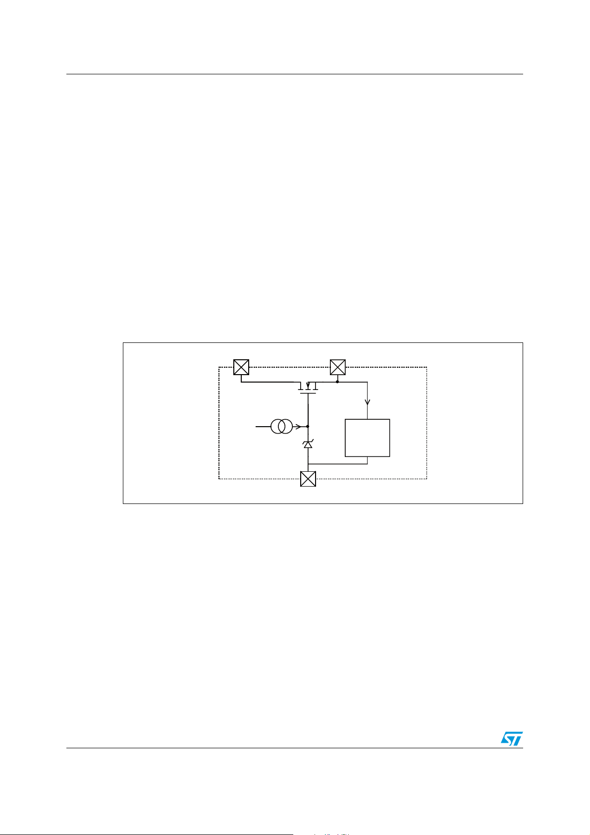
Internal supplies L6460
4 Internal supplies
L6460 includes three internal regulators used to provide a regulated voltage to internal
circuits.
The internal regulators are the following:
- V
- Charge pump regulator.
- V
4.1 V
V
regulator is not intended to provide external current so it must not be used to supply external
loads. An external capacitor must always be connected to this pin (preferably towards
V
Figure 3. V
SupplyInt
3v3
SupplyInt
SupplyInt
Supply
regulator.
regulator.
regulator
is the output of an internal regulator used to supply some internal circuits. This
pin), recommended value is in the range 80 ÷ 120 nF.
SupplyInt
pin
Vsupply
VsupplyInt
L6460
internal
circuits
IS_Int_TYP
L6460
The V
SupplyInt
resistor R
pin may also be externally connected to V
: this allows R
EXT
, particularly when V
EXT
operative supply range, to dissipate power that otherwise would be dissipated inside the
chip. The choice of the optimal resistor depends on the application since it is strictly
depending on both V
and the current used inside the chip (that is changing with the
Supply
chosen configuration).
R
could be chosen by applying this formula: R
EXT
I
max is depending from the chosen configuration and represents the total current needed
S_Int
by the circuits connected to this pin.
For example, with V
30/139 Doc ID 17713 Rev 1
= 32 V and I
Supply
S_Int
GND
pin by means of an external
Supply
is at the max values of the
Supply
EXT
= (V
Supply
min - V
S_Int
max)/(I
S_Int
= 12 mA a typical resistor value is 1 kΩ.
max).

L6460 Internal supplies
E
d
4.2 Charge pump regulator
L6460 implements a charge pump regulator to generate a voltage over V
.This voltage
Supply
is used to drive internal circuits and the external FET driver and cannot be used for any
other purpose.
This circuit is always under the supervisory circuit control, so no regulator can start before
the V
voltage reaches its undervoltage rising threshold. If V
Pump
voltage falls down
Pump
below its under voltage falling threshold, all the regulators will be switched off.
The charge pump circuit is disabled when L6460 is in “low power mode”.
Figure 4. Charge pump block diagram
VSupplyInt
VSupply
C
BOOST
Pump
V
CPH
for VSupply lower than 15V,
external diodes are require
C
FLY
nVPump
Driver
M2
M1
CPL
An example of capacitors value is: C
4.3 V3v3 regulator
V3v3 is the output of an internal regulator used to supply some low voltage internal circuits.
This regulator is not intended to provide external current so it must not be used to supply
external loads. An external capacitor must always be connected from this pin to GND,
recommended value is in the range 80 ÷ 120 nF.
-
CLK
BOOST
= 100 nF and C
FLY
Ref
BOOST
= 1 µF
Doc ID 17713 Rev 1 31/139

Supervisory system L6460
5 Supervisory system
The supervisory circuitry monitors the state of several functions inside L6460 and resets the
device (and other ICs if connected to nRESET pin) when the monitored functions are
outside their normal range. Supervisory circuitry can be divided into three main blocks:
– Power on reset (POR) generation circuitry.
– nRESET (nRST_int) generation circuitry.
– Thermal shut down (TSD) generation circuitry.
POR circuitry monitors the voltages that L6460 needs to guarantee its own functionality;
nRESET circuitry controls if L6460’s main voltages are inside the normal range; TSD is the
thermal shut down of the chip in case of overheating.
5.1 Power on reset (POR) circuit
Power on reset circuit monitors V
set the device is in a stable and controlled status until the minimum supply voltages that
guarantee the device functionality are reached. The output signal of this circuit (in the
following indicated as “POR”) becomes active when V
threshold.
When POR output signal is active, all functions and all flags inside L6460 are set in their
reset state; once POR signal comes back from off state (meaning monitored voltages are
above their rising threshold), the power up sequence is re-initialized.
5.2 nRESET generation circuit
The nRESET circuit monitors V
(V
monitored voltages reach their operative value (please note that V
so it must be above its minimum value, otherwise nRESET circuit is not active).
This circuit generates an internal reset signal (in the following indicated as “nRST_int”) that
will also be signaled to external circuits by pulling low the nRESET pin.
The signal nRST_int becomes active in the following cases:
1. When one of the following voltages is lower than its own under voltage threshold:
2. When watchdog timer counter (see Chapter 6) elapse the watchdog timeout time (only
3. When L6460 is in “Low Power mode”.
4. When EnExtSoftRst bit in SoftResReg register is at logic level = “1” and a “SoftRes”
) voltages. The purpose of this circuit is to prevent the device functionality until the
System
–V
–V
–V
–V
and V
Supply
.
Pump
System
GPIO_SPI
SupplyInt
(all switching or linear system regulators voltages).
.
if watchdog function is enabled).
command is applied (see SoftResReg register description in Chapter 25).
Supply
Supply
.
, and V
, V
SupplyInt
voltages. The purpose of this circuit is to
3V3
, V
Pump
Supply
, V
GPIO_SPI
or V
go under their falling
3V3
and all system regulators
is monitored by POR,
3v3
When an nRST_int event is caused by above cases, the nRESET pin will stay low for a
“stretch” time that starts from the moment that nRST_int signal returns in the operative
32/139 Doc ID 17713 Rev 1

L6460 Supervisory system
state. This stretch time can be selected by setting the ID[1:0] bits in the SampleID register
according to following table.
Table 6. Stretch time selection
Selected stretch time
ID[1] ID[0]
Note
Typ
0 0 16ms Default state
0132ms
1048ms
1164ms
When nRST_int becomes active (logic level = “0”) it sets in their reset state some of the
functions inside L6460. The main functions that will be reset by nRST_int signal are the
following:
– Serial interface will be reset and will not accept any other command.
– The bridges 1 and 2 will place their outputs in high impedance and PWM and
direction signals will be reset.
– AD converter will be powered off.
– GPIOs will be powered off.
– Current DAC will be powered off.
– Operational amplifiers will be powered off.
– Watchdog count will be reset (while Watchdog flags won’t be reset).
– Interrupt controller will be powered off.
– Digital comparator will be powered off.
Additionally the system regulators will be powered off but only if the voltage that caused the
nRST_int event is checked before the system regulator in the power up sequence. This
means that:
– all system regulators will be powered off if nRST_int is caused by V
V
SupplyInt
, V
(and also if V3v3 causes a POR);
Pump
Supply
,
– no one of the system regulators will be powered off if nRST_int is caused by
V
GPIO_SPI
;
– only the system regulators that follows the system regulator that caused the
nRST_int in power up sequence will be powered off.
Doc ID 17713 Rev 1 33/139
Supervisory system L6460
Figure 5. nReset generation circuit
t
nRST_i
V
Supply
V
SupplyInt
V
Pum p
V
V
SysX
SysY
UV comparator
UV comparator
UV comparator
UV comparator
UV comparator
UV Filter
UV Filter
UV Filter
UV Filter
UV Filter
V
Supply
V
SupplyInt
V
Pum p
UV
UV
System
to
SPI
UV
regulators
UV
Low Power
Mode
WD_En_nRst
nt
Elapsed
WatchDog
Filter
nGateCtrl
nRESET
pin Driver
POR
nRESET
pin
Note: All regulator voltages included in power up sequence (V
considered as nRESET circuit voltages.
SysX
– V
in Figure 5) will be
SysY
34/139 Doc ID 17713 Rev 1

L6460 Supervisory system
5.3 Thermal shut down generation circuit
The third component of the supervisory circuit is the thermal shut down generation circuit.
This circuit generates two different flags depending on the IC temperature:
– the “TSD” flag indicates that the IC temperature is greater than the maximum
allowable temperature.
– the “Warm” flag, that can be read using serial interface, becomes active at a lower
temperature respect to TSD signal, therefore it can be used to prevent the IC from
reaching over temperature.
When a TSD event occurs, L6460 will enter in the reset state placing the bridges in high
impedance and turning off all regulators and other circuits until the internal temperature
decreases below the Warm temperature. At this point, L6460 will restart the power up
sequence and TSD bit will be set and will be readable as soon as L6460 will come out from
the reset state.
This TSD bit can be reset in three ways:
– by writing a logic level ‘1’ in the ClearTSD bit in the ICTemp register (see
Chapter 24);
– by a POR event;
– by entering in “Low Power Mode”.
The Warm bit, set by L6460 when IC is working over the warming temperature, can be read
using the SPI interface. Once this bit is set it can be reset in three ways:
– by writing a logic level ‘1’ in the ClearWarm bit;
– by a POR event;
– by entering in “Low Power Mode”.
The thermal sensor voltage can be converted using the internal A/D: this way the
microcontroller can directly measure the IC temperature.
To avoid unwanted commutation especially when temperature is near the thresholds, the
output signal is filtered for both TSD and Warm.
Doc ID 17713 Rev 1 35/139

Watchdog circuit L6460
t
t
g
6 Watchdog circuit
The Watchdog timer can be used to reset L6460 if it is not serviced by the firmware that can
periodically write at logic level “1’ the ClrWDog bit in the WatchDogStatus register.
This circuit is disabled by default; firmware can enable it by setting at logic level ‘1’ the
WDEnable bit in the WatchDogCfg register.
When the Watchdog timeout event happens, L6460 sets to ‘1’ a latched bit WDTimeOut in
theWatchDogStatus register that can be read using SPI interface; once this bit is set it can
be cleared in three ways:
– by writing a ‘1’ in the WDClear bit in the WatchDogStatus register.
– by writing a ‘1’ in the SoftReset bit in the WatchDogStatus register.
– by a POR event.
The Watchdog function includes also a warning bit WDWarning to indicate, via serial
interface or via the circuit called Interrupt Controller (see Chapter 21) that the watchdog is
near to its timeout; this bit is asserted to logic level “1” exactly one watch dog clock period
(WD_Tclk) before the watchdog timeout happens. Firmware can enable the WDTimeOut
signal to cause an “nRst_int” event by setting to logic ‘1’ the WDEnnRst bit.
Figure 6. Watchdog circuit block diagram
Fosc
Frequency divider
WD_clk
ClrWDog
WDEnable
Watchdog counter
WDWarning
WDTimeOut
To SPI
]
WDdelay[3:0
To nRSTint
eneration circuit
WD_req_nRs
WD_En_nRs
The watchdog timeout has an imprecision of maximum one WD_Tclk. The effective
programmed WD time is changed in the register only when the watchdog circuit is serviced
by firmware with ClrWDog bit. At this time the watchdog timer is reset and the new value of
the WD delay value is loaded.
The watchdog timer can be programmed to generate different timeouts using the
WDdelay[3:0] bits in the WatchDogCfg register according to following table.
36/139 Doc ID 17713 Rev 1

L6460 Watchdog circuit
Table 7. Watchdog timeout specifications
WD timeout
WDdelay[3:0]
Typ
0000 8*WD_Tclk
0001 9*WD_Tclk
0010 10*WD_Tclk
0011 11*WD_Tclk
0100 12*WD_Tclk
0101 13*WD_Tclk
0110 14*WD_Tclk
0111 15*WD_Tclk
1000 16*WD_Tclk
1001 17*WD_Tclk
1010 18*WD_Tclk
1011 19*WD_Tclk
1100 20*WD_Tclk
1101 21*WD_Tclk
1110 22*WD_Tclk
1111 23*WD_Tclk
Doc ID 17713 Rev 1 37/139

Internal clock oscillator L6460
7 Internal clock oscillator
L6460 includes a free running oscillator that does not require any external components.
This circuit is used to generate the time base needed to generate the internal timings; the
typical frequency is 16 MHz.
The oscillator circuit starts as soon as the IC exits from the power on reset condition and it is
stopped only when in “low power mode”.
38/139 Doc ID 17713 Rev 1

L6460 Start-up configurations
8 Start-up configurations
L6460 start-up configuration is selected by setting in different states the GPIO[0], GPIO[3]
and GPIO[4] pins. Each of these is a three state input pin and is able to distinguish among
the following situations:
Table 8. Possible start-up pins state symbol
Pin condition State symbol
Shorted to ground 0
Shorted to V
Floating Z
Note: “Shorted” means: R≤1KOhm; “Z” means: R≥10KOhm, C≤200pF
8.1 Operation modes
pin 1
3v3
When V
voltage is applied to L6460, the internal regulator V3v3, used to supply the
Supply
logic circuits inside the device, starts its functionality. When it reaches its final value, L6460
enables the GPIO[0] pin state read circuitry, and, after a time TpinSample, it will sample the
GPIO[0] state. If it is found to be in high impedance, L6460 does not consider GPIO[3] and
GPIO[4] pins state and starts its “Basic device” mode sequence. If GPIO[0] is found to be
connected to ground or to V3v3, L6460 checks the state of GPIO[3] and GPIO[4] pins to
select its start-up configuration.
The possible configurations can be classified in four “Major” modes:
1. Basic device.
2. Slave device.
3. Master device.
4. Single device.
Hereafter is reported the correspondence table between GPIO[X] state and L6460
configurations.
Doc ID 17713 Rev 1 39/139
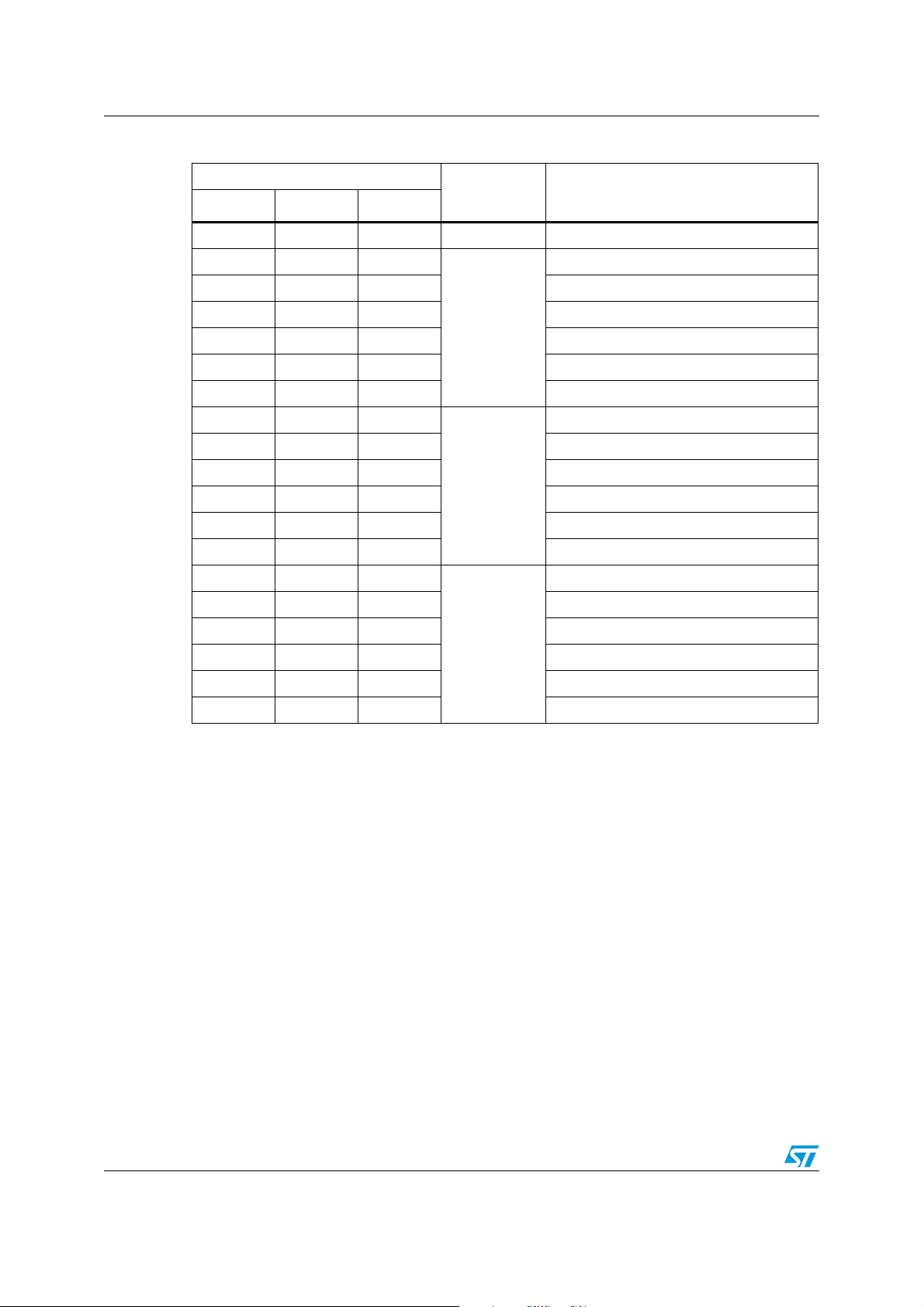
Start-up configurations L6460
Table 9. Start-up correspondence
Pin state
GPIO[0] GPIO[3] GPIO[4]
ZXXBasic
000
0 0 Z Primary regulator
001 Regulators
0 Z 0 Simple regulator
0 Z Z Bridge + VEXT
0 Z 1 Secondary regulators
010
0 1 Z Primary regulator
011 Regulators
1 0 0 Simple regulator
1 0 Z Bridge + VEXT
1 0 1 Secondary regulators
(1)
Major mode Minor mode
Bridge
Single
Bridge
Master
(2)
(3)
(3)
1Z0
1 Z Z Primary regulator
1 Z 1 Regulators
1 1 0 Simple regulator
1 1 Z Bridge + VEXT
1 1 1 Secondary regulators.
1. “X” means “don’t care”.
2. The description of these modes is in the following Chapter 8.6
3. VEXT is the regulator output voltage obtained using the switching regulator controller with external FET.
8.2 Basic device mode
The basic device mode is selected by leaving the GPIO[0] pin floating. In this mode L6460
doesn’t use GPIO[3] and GPIO[4] as configuration pins, leaving them free for other uses.
When in this mode the regulators included in the start up sequence (except V
considered as system regulators and they start in the following sequence:
1. Auxiliary switching regulator1 (V
2. Auxiliary switching regulator2 (V
3. Main linear regulator (V
4. Main switching regulator (V
SWmain
SWmain
Slave
AUX1_SW
AUX2_SW
).
).
).
) (Not system regulator).
Bridge
(3)
SWmain
) are
40/139 Doc ID 17713 Rev 1

L6460 Start-up configurations
8.3 Slave device mode
In slave device mode, L6460 consider the nAWAKE pin as an input enable. Since this is now
a digital pin, the current pull up source inside the nAWAKE circuit is disabled.
At the startup, if the nAWAKE pin is found to be low for a period higher than t
L6460 enters directly in the “Low Power mode”; when nAWAKE pin is pulled high for a
period higher than t
AWAKEFILT
, L6460 begins its start up procedure.
8.4 Master device mode
In master device mode, L6460 begins its start up procedure without waiting for any external
enable signal and it uses GPIO[5] pin to drive the nAWAKE pin of Slave devices.
During the whole start up time, it forces its GPIO[5] pin at logic level “0” in order to maintain
all slave devices in “Low Power mode” as previously described. When start up operations
are completed, L6460 forces the GPIO[5] output to logic level “1” to enable the slave devices
and keeps GPIO[5] output at high level until it senses an under-voltage on any of its System
regulators. If firmware writes in the PwrCtrl register to set Master L6460 in “Low Power
mode” it immediately forces GPIO[5] output to logic level “0” to force the slave devices to
enter in “Low Power mode”, then it waits for T
mode” sequence.
8.5 Single device mode
In single device mode, the device behaves similarly to master device mode but:
1. It doesn’t use the GPIO[5] pin to drive slave devices.
2. It doesn’t wait for T
MASTWAIT
before entering in “Low Power mode”.
MASTWAIT
AWAKEFILT
,
time and it starts its “Low Power
8.6 Sub-configurations for slave, master or single device modes
Each slave, master or single device modes can be divided in other minor modes depending
on the start-up sequence needed for L6460 internal regulators.
Unless otherwise specified, in all the following modes the regulators included in the start up
sequence are considered system regulators and they start in the sequence indicated.
8.6.1 Bridge mode
In this configuration bridges 3 and 4 are not used as regulators and therefore can be
configured by the firmware in any of their possible bridge modes.
When in this mode the power-up sequence is:
1. Main switching regulator (V
2. Main linear regulator (V
LINmain
Doc ID 17713 Rev 1 41/139
SWmain
).
).

Start-up configurations L6460
8.6.2 Primary regulator mode (KP)
In this configuration bridge 4 can be configured by firmware while bridge 3 is configured as
two separate synchronous switching regulators. The last regulator in the sequence
(V
AUX2_SW
) is not considered a system regulator.
When in this mode the power-up sequence is:
1. Auxiliary switching regulator1 (V
2. Main switching regulator (V
SWmain
3. Auxiliary switching regulator2 (V
AUX1_SW
AUX2_SW
).
) together with main linear regulator (V
) (Not system regulator).
LINmain
).
8.6.3 Regulators mode
In this configuration bridge 4 can be configured by firmware while bridge 3 is configured as
two separate synchronous switching regulators, but the start up sequence is different
previous one.
When in this mode the power-up sequence is:
1. Main switching regulator (V
2. Auxiliary switching regulator1 (V
3. Auxiliary switching regulator2 (V
SWmain
AUX1_SW
AUX2_SW
).
)
)
8.6.4 Simple regulator mode (KT)
Also in this configuration bridge 4 can be configured by firmware while bridge 3 is configured
as two separate synchronous switching regulators. The last regulator in the sequence
(V
When in this mode the power-up sequence is:
1. Auxiliary switching regulator1 (V
2. Auxiliary switching regulator2 (V
3. Main linear regulator (V
4. Main switching regulator (V
8.6.5 Bridge + V
In this configuration bridges 3 and 4 are not used as regulators and the regulator obtained
using the switching regulator controller (V
When in this mode the power-up sequence is:
1. Main switching regulator (V
2. Switching regulator controller regulator (V
3. Main linear regulator (V
) is not considered a system regulator.
SWmain
LINmain
SWmain
mode
EXT
SWmain
LINmain
AUX1_SW
AUX2_SW
).
)
)
) (not system regulator).
) is included in start-up.
SWDRV
).
SWDRV
).
).
42/139 Doc ID 17713 Rev 1

L6460 Start-up configurations
8.6.6 Secondary regulators mode
In this configuration, bridge 3 is configured as a single synchronous switching regulator
using its two half bridges in parallel (V
AUX_(1//2)SW
When in this mode the power-up sequence is:
1. Main switching regulator (V
2. Auxiliary switching regulator (V
3. Main linear regulator (V
LINmain
SWmain
AUX(1//2)_SW
).
).
).
).
Doc ID 17713 Rev 1 43/139

Power sequencing L6460
9 Power sequencing
As soon as V
charge pump circuit; once V
Supply
and V
SupplyInt
Pump
are above their power on reset level, L6460 will start the
voltage reaches its under voltage rising threshold, L6460
begins a sequence that starts the regulators considered system regulators.
A regulator is considered a System regulator if:
– It has to start in on state without any user action.
– It is included in the power-up sequence.
– Its under-voltage event is considered by L6460 as an error condition to be
signaled through nRESET pin.
Once V
Supply
and V
SupplyInt
, V
and all the system regulators are over their under
Pump
voltage rising threshold, L6460 enters in the normal operating state, that will release
nRESET pin and will wait for SPI commands.
L6460 will reduce the noise introduced in the system by switching out of phase all its power
circuits (switching regulators, bridges and charge pump).
The L6460's startup sequence of operation is the following:
– start V
internal linear regulator
3v3
– sample startup configuration
– wait enable if slave device
– start charge pump
– start system regulators (see order in Section 8.6)
– if master send enable to slave device
– wait until V
GPIO_SPI
becomes ok
44/139 Doc ID 17713 Rev 1

L6460 Power saving modes
1
10 Power saving modes
Saving power is very important for today platforms: L6460 implements different functions to
achieve different levels of power saving. Sections here below describe these different power
saving modes.
10.1 Standby mode
Almost all low voltage circuitry inside L6460 are powered by V
regulator is a linear regulator powered by V
by V
regulator is directly coming from V
3v3
SupplyInt.
SupplyInt
This means that all the current provided
and therefore the total power
internal regulator; this
3v3
consumption is:
Low voltage power = V
because V
SupplyInt
is feeded by V
, directly or with a resistor in series.
Supply
This power could be reduced by using a switching buck regulator to supply V
Supply
* I
V3v3
.
: in this
3v3
case, assuming the buck regulator efficiency near to 100%, the dissipated power would
become:
Low voltage power ≈ 3.3V * I
To achieve this result there is the need to switch off the internal V
V3v3
.
linear regulator and to
3v3
use an additional pin to provide a 3.3 V supply to internal circuits. L6460 can do this by
using the low voltage switch implemented on GPIO6 pin. This switch internally connects
V
GPIO_SPI
V
GPIO_SPI
voltage to GPIO6 output so, by externally connecting GPIO6 to V
voltage can be provided to low voltage circuitry inside L6460.
pin, the
3v3
Figure 7. Standby mode function description
VSupplyInt
VGPIOSpi
StdByMode
3.3 V
1.9 V
The StdByMode bit used to switch off V
by writing the standby command in the StdByMode register. L6460 exits standby mode if a
0
+
1
-
V3v3
Regulator
and switch on the power switch can be set to ‘1’
3v3
Power Switch
GPIO6
External
connection
3.3V
reset event happens or “Low Power mode” is selected.
Because all internal low voltage circuitry powered by V
voltage rail, when the standby mode is used, V
Doc ID 17713 Rev 1 45/139
GPIO_SPI
are designed to work with a 3.3V
3v3
is requested to be at 3.3V.

Power saving modes L6460
10.2 Hibernate mode
L6460’s hibernate mode allows the firmware to switch off some (or all) selected System
Regulators leaving in on state only those necessary to resume L6460 to operative condition
when waked-up by an external signal.
Hibernate mode is selected when the firmware writes the command word in the
HibernateCmd register. When in hibernate mode L6460 will force regulators in the state
(on/off) selected by the firmware by writing in the HibernateCmd register and will force
nRESET pin low.
The exiting from hibernate mode is achieved by forcing at low level nAWAKE pin (or GPIO5
pin if L6460 is in Slave mode); L6460 will also exit from hibernate mode if an undervoltage
event happens on V
Supply
, V
SupplyInt
, V
Pump
or V
3v3
.
When the exit from hibernate mode is due to an external command, L6460 sets to ‘1’ the bit
HibModeLth in the HibernateStatus register.
10.3 Low power mode
When in normal operating mode, the microcontroller can place L6460 in “Low Power mode”.
In this condition L6460 sets all bridges outputs in high impedance, powers down all
regulators (including system regulators and charge pump) and disables almost all its circuits
including internal clock reducing as much as possible power consumption.
The only circuits that remain active are:
–V
internal regulator.
3V3
– nAWAKE pin current pull-up.
– nRESET pin that will be pulled low.
– POR circuit.
The entering in low power mode is obtained in different ways depending if L6460 is
configured as slave device or not. When L6460 is configured as slave device the low power
mode is directly controlled by nAWAKE pin that acts as an enable: if this pin is low for a time
longer then t
AWAKEFILT
Power mode.
In all other start-up configurations, Low Power mode is entered by writing a Low Power
mode command in the PowerModeControl register; once L6460 is in Low Power mode it
starts checking the nAWAKE pin status: if it is found low for a time longer than t
L6460 exits from Low Power mode and restarts its startup sequence. When the nAWAKE
pin is externally pulled low, the “AWAKE” event is stored and it is readable through SPI.
L6460 will also exit from Low Power mode if a POR event is found.
Note: When in “Low power mode” V
10.4 nAWAKE pin
At the start up, before L6460 has identified the required operation mode (see Chapter 8), a
current sink I
is always active to pull down nAWAKE pin. As soon as the operation mode
INP
(basic, slave, master or single device) is detected, the functionality of nAWAKE pin will be
different.
, Low Power mode is entered; if this pin is high L6460 exits from Low
,
is monitored only for its power on reset level.
Supply
AWAKEFILT
46/139 Doc ID 17713 Rev 1

L6460 Power saving modes
If L6460 is not configured as slave device a current source I
while the current sink I
current sink I
will be active until nAWAKE pin is detected high for the first time; after that
INP
both current sources I
will be disabled. If L6460 is configured as a Slave device, the
INP
INP
and I
will be disabled and the nAWAKE pin can be considered
OUT
OUT
as a digital input.
Here below is reported the nAWAKE pin simplified schematic.
Figure 8. nAWAKE function block diagram
V
3v3
SlaveMode
I
OUT
AWAKE_req
AWAKE
nAWAKE seen high
for the first time after
start up.
I
INP
will be active on this pin,
Doc ID 17713 Rev 1 47/139

Linear main regulator L6460
11 Linear main regulator
The linear main regulator is directly powered by V
voltage and it is one of the
Supply
regulators that L6460 could consider as a system regulator. This means that the voltage
generated by this regulator is not used to power any internal circuit, but L6460 will check
that the feedback voltage V
LINmain_FB
internal functions. When an under-voltage event (with a duration longer than period t
is in the good value range before enabling all its
prim_uv
defined by the deglitch filter) is detected during normal operation, L6460 will enter in reset
state and it will signal this event to the microcontroller by pulling low the nRESET pin and
disabling most of its internal blocks.
Here are summarized the primary features of the regulator:
– Regulated output voltage from 0.8V to V
-2V with a maximum load of 10mA.
Supply
– Band gap generated internal reference voltage.
– Short circuit protected (output current is clamped to 22mA typ).
– Under voltage signal (both continuous and latched) accessible through serial
interface.
– Low power dissipation mode.
The internal series element is a P-channel MOS device. The voltage regulator will regulate
its output so that feedback pin equals V
LINmain_FB
, therefore the regulated voltage can be
calculated using the formula:
V
LINmain_OUT
= V
LINmain_ref
*(Ra+Rb)/R
b
Figure 9. Linear main regulator
To extend the output current capability this regulator can be used as a controller for an
V
supply
Body Diode
Driver
+
-
V
LINmain_ref
V
LINmain_OUT
V
LINmain_FB
Cc
Ra
Rb
external active component able to provide higher current (i.e. a Darlington device); the
external power element allows the handling of an higher current since it dissipates the
power externally (the power dissipated by a linear driver supplied at V
voltage V
LINmain_OUT
with an output current I
is about: Pd= (V
OUT
Supply-VLINmain_OUT
and regulating a
Supply
)*I
OUT
.
48/139 Doc ID 17713 Rev 1

L6460 Linear main regulator
Figure 10. Linear main regulator with external bipolar for high current
V
supply
Body Diode
V
LINmain_OUT
Driver
+
V
LINmain_Ref
V
LINmain_FB
C
load
R
R
Whichever configuration is used (regulator or controller), a ceramic capacitor must be
connected on the output pin towards ground to guarantee the stability of the regulator; the
value of this capacitance is in the range of 100 nF to 1 µF depending on the regulated
voltage;
● V
LINmain_OUT
● 0.8V< V
● 2.5V= V
● V
LINmain_OUT
= 0.8 V --> 1 µF
LINmain_OUT
LINmain_OUT
> 5 V --> 0.1 F
< 2.5 V --> 0.68 µF
5 V --> 0.33 µF
When this regulator is disabled, the whole circuit is switched off and the current
consumption is reduced to a very low level both from V3v3 and from V
. When in this
Supply
condition, the output pin is pulled low by an internal switch.
Doc ID 17713 Rev 1 49/139

Main switching regulator L6460
12 Main switching regulator
Main switching regulator is an asynchronous switching regulator intended to be the source
of the main voltage in the system. It implements a soft start strategy and could be a system
regulator so even if its output voltage V
SWmain
L6460 will check that it is in the good value range before enabling all its internal functions.
When L6460 detects a system regulator under-voltage event with a duration longer than the
period defined by the deglitch filter (t
prim_uv
the microcontroller by pulling low the nRESET pin and disabling most of its internal block
(e.g. bridges, GPIOs, …).
The output voltage will be externally set by a divider network connected to feedback pin. To
reduce as much as possible the regulation voltage error L6460 has the possibility to choose
between four feedback voltage references (and, as a consequence, four under-voltage
thresholds) using the serial interface. The feedback reference voltage selection is made by
writing the SelFBRef bits in the MainSwCfg register.
Here after are summarized the primary features of this regulator:
– Internal power switch.
– Soft start circuitry to limit inrush current flow from primary supply.
– Internally generated PWM (250 kHz switching frequency).
– Nonlinear pulse skipping control.
– Protected against load short circuit.
– Cycle by cycle current limiting using internal current sensor.
– Under voltage signal (both continuous and latched) accessible through SPI.
is not used to power any internal circuit,
), it will enter in reset state signaling this event to
When L6460 is in “low power mode”, this regulator will be disabled.
In order to save external components and power when using two or more L6460 IC’s on the
same board, the primary switching regulator can be disabled by serial interface. Care must
be paid using this function because an under-voltage on this regulator, as previously seen,
will be read as a fault condition by L6460.
12.1 Pulse skipping operation
Pulse skipping is a well known, non linear, control strategy used in switching regulators.
In this technique (see Figure 11) the feedback comparator output is sampled at the
beginning of each switching cycle. At this time, if the sampled value shows that output
voltage is lower than requested one, the complete PWM duty cycle is applied to power
switch; otherwise no PWM is applied and the switching cycle is skipped. Once PWM is
applied to power element only a current limit event can disable the power switch before the
whole duty cycle is finished.
50/139 Doc ID 17713 Rev 1

L6460 Main switching regulator
Figure 11. Main switching regulator functional blocks
VSupply
Current Sense
Driver
Regulator Ref
Regulator Freq
Voltage
Loop Control
+
VSWmain_SW
VSWmain_FB
La
Ra
C
R
b
From Central Logic
Control
Logic
Charge pump Voltage
High Side
Under voltage flag
To Central Logic
Filter
+
Under voltage
Threshold
In pulse skipping control the duty cycle must be chosen by the user depending on supply
voltage and output regulated voltage. Therefore the switching regulator has 4 possible duty
cycles that can be changed by writing the VmainSwSelPWM bits in the MainSwCfg register
according to following Ta bl e 1 0.
Table 10. Main switching regulator PWM specification
MainSwCfg register Duty cycle value
Comments
VmainSwSelPWM[1:0] Typical
00 12%
01 15%
10 26% Default state
11 63.5%
The output current is limited to a value that can be set by means of SelIlimit bit in the
MainSwCfg register according to following Tab l e 1 1 .
Table 11. Main switching regulator current limit
SelIlimit Current limit (min) Comments
0 3.3A Default state
12.3A
Doc ID 17713 Rev 1 51/139

Switching regulator controller L6460
13 Switching regulator controller
This circuit controls an external FET to implement a switching buck regulator using a non
linear pulse skipping control with internally generated PWM signal.
The output voltage will be externally set by a divider network connected on feedback pin. To
reduce as much as possible the regulation voltage error L6460 has the possibility to switch
between four regulator feedback voltage references (and, as a consequence, four undervoltage thresholds) using serial interface. The feedback reference voltage is selected by
writing the SelFBRef bits in the SwCtrCfg.
This regulator is switched off when L6460 is powered up for the first time and can be
enabled using L6460’s SPI interface.
Here after are summarized the main features of the regulator:
– Soft start circuitry to limit inrush current flow from primary supply.
– Changeable feedback reference voltage
– Internally generated PWM (250 kHz switching frequency).
– Nonlinear pulse skipping control.
– Protected against load short circuit.
– Cycle by cycle current limiting using internal current sensor.
– Under voltage signal (both continuous and latched) accessible through SPI.
52/139 Doc ID 17713 Rev 1

L6460 Switching regulator controller
V
out
y
Figure 12. Switching regulator controller functional blocks
V
suppl
R
sense
N-CH Fet
La
Ra
C
R
b
From Central Logic
SelFBRef[1:0]
Vref = 3 V
Vref = 3V
Vref=0.8 V
Vref=0.8 V
Control
Logic
under voltage flag
To Central Logic
SelFBRef
Charge pump Voltage
Analog Mux
Filter
Uv Threshold 1
Uv Threshold 2
Driver
Regulator Freq
VFBRef
Analog Mux
Current Sense
Voltage
Loop Control
+
Under voltage
Threshold
V
SWDRW_sns
V
SWDRV_gate
V
SWDRV SW
-
+
V
SWDRV FB
13.1 Pulse skipping operation
Pulse skipping strategy has already been explained on main switching regulator section.
This regulator has 4 possible PWM duty cycles that can be changed writing in the
SelSwCtrPWM bits in the SwCtrCfg register using SPI.
Table 12. Switching regulator controller PWM specification
SwCtrCfg register Duty cycle value
SelSwCtrPWM[1:0] Typical
00 9%
01 12%
10 22.5% Default state
11 58%
Comments
Doc ID 17713 Rev 1 53/139

Switching regulator controller L6460
13.2 Output equivalent circuit
The switching regulator controller output driving stage can be represented with an
equivalent circuit as in the Figure 13:
Figure 13. Switching regulator controller output driving: equivalent circuit
VPUMP
I
SOURCE
Source command
Tsink
V
SWDRV_gate
Sink pulse command
R
SUSTAIN
Sink command
I
SINK
V
SWDRV_SW
As can be seen from the above figure, the external switch gate is charged with a current
generator I
SOURCE
applied for a T
and it is discharged towards ground with a current generator I
pulse while an equivalent resistor R
SINK
SUSTAIN
is connected between gate
SINK
and source until the sink command is present.
13.3 Switching regulator controller application considerations
This controller can implement a step-down switching regulator used to provide a regulated
voltage in the range 0.8 V – 32 V. Such kind of variation could be managed by considering
some constraints in the application and particularly by choosing the correct feedback
reference voltage as indicated in the Tab le 1 3 .
Table 13. Switching regulator controller application: feedback reference
that is
Output regulated voltage range Feedback voltage reference
0.8V ≤ V
5V ≤ V
< 5V 0.8V - 1V
out
≤ 32V 2.5V - 3V
out
54/139 Doc ID 17713 Rev 1

L6460 Switching regulator controller
An example of application can be considered the following, supposing the external mosfet
type STD12NF06L:
– Max DC current load = 3 A
– Typ Over current threshold = 3 A * 1.5 = 4.5 A
– L = 150 µH
– C = 220-330 µF
In this conditions the step-down regulator will result over-load protected, short-circuit
protected over all the regulated voltage range and the V
Supply
range.
Other application configurations could be evaluated before being implemented.
Doc ID 17713 Rev 1 55/139

Power bridges L6460
14 Power bridges
L6460 includes four H bridge power outputs (each one made by two independent half
bridges) that are configurable in several different configurations.
Each half bridge is protected against: over-current, over-temperature and short circuit to
ground, to supply or across the load. When an over current event occurs, all outputs are
turned off (after a filter time), and the over current bit is stored in the internal status register
that can be read through SPI.
Positive and negative voltage spikes, which occur when switching inductive loads, are
limited by integrated freewheeling diodes (see Figure 14).
Figure 14. H Bridge block diagram
7TVQQMZ
(IGHSIDE
$RIVER
,OWSIDE
$RIVER
#ON T R OL ,O G I C
#ON T R OL ,O G I C
(I
GHSIDE
$RIVER
,OW S ID E
$RIVER
(/%
PS
4&/4&
During the start up procedure the bridges are in high impedance and after that they can be
enabled through SPI. When a fault condition happens, i.e. an over-temperature event, the
bridges return in their start-up condition and they need to be re-enabled from the micro
controller.
The bridges can use PWM signals internally generated or externally provided (supplied
through the GPIO pins). Internally generated PWM signals will run at approximately
31.25kHz with a duty cycle that, through serial interface, can be programmed and
incremented in steps of 1/(512*F
). To reduce the peak current requested from supply
osc
voltage when all bridges are switching, the four internally generated PWM signals are outof-phase.
Each half bridge will use the PWM signal selected by the respective
MtrXSelPWMSideY[1:0] (X stands for 1, 2, 3 or 4; Y stands for A or B) bits in the SPI, but if
two half bridges are configured as a full bridge, only the PWM signal chosen for side A will
be used to drive the resulting H bridge.
More in detail the PWM selection truth table will be as describe in the following tables:
56/139 Doc ID 17713 Rev 1

L6460 Power bridges
Table 14. PWM selection truth table for bridge 1 or 2
MtrXSelPWMSideY [1] MtrXSelPWMSideY [0] Selected PWM
(1)
00
01
MotorXPWM (Configurable by means of MtrXCfg
register).
AuxXPWM (Configurable by means of
AuxPwmXCtrl register).
1 0 ExtPWM1 (from GPIO 9 input)
1 1 ExtPWM2 (from GPIO 10 input)
1. In this table X stands for 1 or 2, Y stands for A or B.
Table 15. PWM selection truth table for bridge 3 or 4
MtrXSelPWMSideY [1] MtrXSelPWMSideY [0] Selected PWM
00
01
MotorXPWM (Configurable by means of
MtrXCfg register).
AuxXPWM (Configurable by means of
AuxPwmXCtrl register).
(1)
1 0 ExtPWM3 (from GPIO 2 input)
1 1 ExtPWM4 (from GPIO 11 input)
1. In this table X stands for 3 or 4, Y stands for A or B.
In Figure 15 is reported a block diagram representing the possible PWM choices for each
L6460 half bridges. The figure is related only to bridges 1 and 2, but it could be assumed to
be valid also for bridges 3 and 4, with few differences due to different possible configurations
of these last drivers.
Doc ID 17713 Rev 1 57/139
Power bridges L6460
Figure 15. Bridge 1 and 2 PWM selection
Mtr1SelPWMSide A[1:0]
00 Motor1 PWM
01 Aux1PWM
10 ExtPWM1
11 ExtPWM2
Mtr1SelPWMSideB [1:0]
00 Motor1 PWM
01Aux1PWM
10ExtPWM1
11ExtPWM2
Mtr2SelPWMSideA[1:0]
00 Motor2 PWM
01Aux2Pwm
10ExtPwm1
11ExtPwm2
Mtr2SelPWMSide B [1:0]
00 Motor2 PWM
01 Aux2Pwm
10 ExtPwm1
Motor 1 side A
Mtr1_2Parallel
Mtr1Tablel[1:0]
Motor 1 sideB
Bridge1
Mtr1_2Parallel
Mtr2Tablel[1:0]
Mtr1_2Parallel
Mtr2Tablel[1:0]
Logic Table
Side A Power Section
Logic Table
Side B Power Section
Motor2 side A
Logic Table
Side A Power Section
Motor 2 sideB
Logic Table
11 ExtPwm2
58/139 Doc ID 17713 Rev 1
Bridge2
Side B Power Section
L6460 Power bridges
14.1 Possible configurations
The selection of the bridge configuration is done through SPI, by writing the MtrXTable[1:0]
bits in the MtrXCfg register. The table below shows the correspondence between
MtrXTable[1:0] bits and the bridge configuration.
Table 16. Bridge selection
MtrXTable[1] MtrXTable[0] Bridge configuration
00Full bridge
0 1 High or low side switch
1 0 Half bridge
1 1 High or low side switch
Bridge 1 & 2 can be paralleled by means of Mtr1_2Parallel bit in the Mtr1_2Cfg register:
Bridge 1 and 2 paralleled will form superbridge1, bridge X side A and bridge X side B
paralleled form SuperHalfBridgeX or SuperSwitchX.
Bridge 3 & 4 can be configured by means of Mtr3_4CfgTable[1:0] bits in the Mtr3_4Cfg
register according to following table:
Table 17. Bridge 3 and 4 configuration
Mtr3_4CfgTable[1] Mtr3_4CfgTable[0] Bridge 3 and 4 configuration
0 0 Two independent bridges
0 1 Two bridges in parallel
1 0 Stepper motor
1 1 Stepper motor
The possible configurations for the bridges are described in the following.
Doc ID 17713 Rev 1 59/139

Power bridges L6460
14.1.1 Full bridge
When in full bridge configuration, the drivers will behave according to the following truth
table:
Table 18. Full bridge truth table
TSD nRESET
Low
power
mode
Enable
Current
limit
MtrXCtrl
SideA
MtrXCtrl
SideB
PWM OUT+ OUT-
1X XXXX XXZZ
00 X XXX XXZZ
01 1 XXX XXZZ
01 0 0XXXXZZ
01 0 11 X XXZZ
01 0 10 0 0 X00
01 0 10 0 1 011
01 0 10 0 1 101
01 0 10 1 0 011
01 0 10 1 0 110
01 0 10 1 1 X11
Note: Note: When “low power mode” is active, the bridges will enter in low power state and will
reduce its biasing thus contributing to the power saving.
When a current limit event occurs this event will be latched and the bridges will remain in
high impedance state for the off time.
60/139 Doc ID 17713 Rev 1

L6460 Power bridges
14.1.2 Parallel configuration (super bridge)
Bridges 1, 2, 3 and 4 can be configured to be used two by two (1 plus 2, 3 plus 4) as one
super bridge thus enabling the driving of loads (motors) requiring high currents. In this
configuration the half bridges will be paralleled and will work as one phase of the superbridge just created: the two phases + will become phase + of the newly created superbridge while the two phases - will become phase –.
Figure 16. Super bridge configuration
Parallel Full Bridge
Super Bridge
Super Bridge
Bridge 1 (3)
Bridge 1 (3)
Bridge 2 (4)
Bridge 2 (4)
M
M
PH
PH
-
-
PH
PH
+
+
PH
PH
+
+
PH
PH
-
-
When this configuration is chosen for bridges 1 (3) and 2 (4), the resulting bridge will use the
driving logic of bridge 1 (3) so for programming it must be used the bridge 1 (3) control and
status bits (direction, PWM, ...): i.e. the used PWM signal will be chosen by
Mtr1SideAPwmSel[1:0] (Mtr3SideAPwmSel[1:0]) bits in SPI.
If the bridges are not configured to be used in parallel, each side of the bridge will use the
PWM selected by the respective MtrXPWMYSel[1:0] bits in the SPI, but if one of the two
drivers is configured as a full bridge only one of the two selected PWM will be used to drive
the motor and this is the PWM chosen for side A.
In order to avoid any problem coming from different propagation times of PWM signals the
anti-crossover dead times are slightly increased when the bridges are paralleled.
14.1.3 Half bridge configuration
Each bridge can be configured to be used as 2 independent half bridges or as 1 super half
bridge (see Figure 17). It is also possible to parallel more than one bridge and use all of
them as a single super half bridge.
Doc ID 17713 Rev 1 61/139

Power bridges L6460
Low side
Driver
Figure 17. Half bridge configuration
V
Supply
V
pump
High side
Driver
Control Signals
From SPI
Control
Logic
Fault
Signals
DCX Phase output
In this case each half bridge will behave according to the following truth table.
Table 19. Half bridge truth table
Low
TSD nReset
power
Enable
mode
1XXXXXXZ
00XXXXXZ
011XXXXZ
0100XXXZ
0101000Z
Current
limit
MtrXCtrl
SideA/B
PWM OUT
01010010
0101010Z
01010111
01011XXZ
Note: When “low power mode” bit is active the bridges will reduce its biasing thus contributing to
the power saving.
When a current limit event occurs this event will be latched and the bridges will remain in
62/139 Doc ID 17713 Rev 1
high impedance state for the off time.
L6460 Power bridges
14.1.4 Switch configuration
Each bridge can be configured to be used as 2 independent switches that connects the
output to supply or to ground. It is also possible to parallel the two switches and use them as
a single super switch.
All resulting switches will behave according to the following truth table.
Table 20. Switch truth table
TSD nReset
Low
power
mode
Enable
Current
limit
MtrXCtrl
SideA/B
PWM OUT
1XXXXXXZ
00XXXXXZ
011XXXXZ
0100XXXZ
010100XZ
01010101
01010110
01011XXZ
Note: When “low power mode” bit is active the bridge will reduce its biasing thus contributing to the
whole power saving.
When a current limit event occurs this event will be latched and the bridge will remain in high
impedance state for the toff time.
14.1.5 Bipolar stepper configuration
The bridges 3 and 4 can be configured to be used as a micro-stepping, bidirectional driver
for bipolar stepper motors.
The primary features of the driver are the following:
– Internal PWM current control.
– Micro stepping.
– Fast, mixed and slow current decay modes.
Each H-bridge is controlled with a fixed and selectable off-time PWM current control circuit
that limits the load current to a value set by choosing V
internal DAC and an the external R
SENSE
value.
STEPREF
voltage by means of the
The max current level could be calculated using the formula:
I
MAX=VSTEPREF/RSENSE
To obtain the best current profile, the user can choose three different current decay modes:
slow, fast and mixed. Initially, during Ton, a diagonal pair of source and sink power MOS is
enabled and current flows through the motor winding and the sense resistor. When the
voltage across the sense resistor reaches the programmed DAC output voltage, the control
logic will change the status of the bridge according to the selected decay mode (slow, fast or
mixed). In slow decay mode the current is recirculated through the path including both high
Doc ID 17713 Rev 1 63/139

Power bridges L6460
side power MOS for the whole off time. In fast decay mode the current is recirculated
through the high and low side power MOS opposite respect to those forcing current to
increase. Mixed decay mode is a selectable mix of the previous two modes (fast decay
followed by slow decay) and allows the user to find the best trade off between load current
ripple and fast current levels transition. Additionally, by setting the
SeqMixedOnlyInDecreasingPh bit in the StpCfg1 register, the user can choose to apply the
fast decay percentage in mixed mode always or only when the current is decreasing (i.e
from 90° to 180° and from 270° to 360° of the sinusoidal wave).
By using SPI interface the user can choose:
● Control type (external firmware control, half step, normal drive, wave drive, micro-step).
● Up to 16 current levels (quasi-sinusoidal increments) for each bridge.
● Current direction.
● Decay mode.
● Blanking time.
● Off time (32 values from 2µs to 64µs).
● Percentage of fast decay respect to toff (when in mixed decay mode).
64/139 Doc ID 17713 Rev 1

L6460 Power bridges
e
y
e
y
r
Figure 18. Bipolar stepper configuration
DC3
SENSE
VRefA
- Control Logic
- Toff generation
- DAC reference
selection
DC3
PH-
_PH-
V
supply
Suppl
Sens
Bridge Driver
Bridge Drive
DC3
PH+
_PH+
PH-
Stepper
Motor
Suppl
Sens
PH+
DC4
-
DC4
Ref1
Ref2
V
STEPREF
VRefB
VRefA
DC4
StepperDACPhA
SelStepRef
StepperDACPhB
VRefB
Using the StepCtrlMode[2:0] bits in StepCfg1 register, L6460 can be programmed to
internally generate the stepping levels. In these cases and depending on the StepFromGpio
bit in the StpCfg1 register the Stepper driver will move to next step each time the StepCmd
bit is set at logic level “1” or at each pulse transition longer than ~1µs externally applied on
GPIO12 (StepReq signal), according to Tab le 2 1 .
Doc ID 17713 Rev 1 65/139
Power bridges L6460
Table 21. Sequencer driver
StepFromGpio Sequencer driver
0 StepCmd bit in StepCmd register.
1 GPIO12 input pin.
The allowable control modes are as follows:
1. Stepping sequence left to external microcontroller: in this mode the current level in
each motor winding is set by the microcontroller via the serial interface.
2. Full step: in this mode the electrical angle will change by 90° steps at each StepReq
signal transition. There are two possibilities:
– Normal step (two phases on): in normal step mode both windings are energized
simultaneously and the current will be alternately reversed. The resulting electrical
angles will be 45°, 135°, 225° and 315°.
– Wave drive (one phase on): In wave drive mode each winding is alternately
energized and reversed. The resulting electrical angles will be 90°, 180° and 270°
and 360°.
3. Half step: in this mode, one motor winding is energized and then two windings
alternately so the electrical angles the motor will do when rotating in clockwise direction
and using the same current limit in both the phases are: 45°, 90°, 135°, 180°, 225°,
270°, 315° and 360°.
4. Microstepping: in this mode the current in each motor winding has a quasi sinusoidal
profile. The increment between each step is obtained at each transition of StepCmd bit
in StepCmd register. The difference between each step could be chosen (4, 8 or 16
levels for each phase) according to following table:
Table 22. Stepper driving mode
StepCtrlMode[2:0] Control mode Description
000 or 111 No Control
Stepping sequence control left to the external
controller
001 Half Step Half step
010 Normal Step Full step (two phases on)
011 Wave Drive Full step (one phase on)
100 1/4 Step Four micro steps
101 1/8 Step Eight micro steps
110 1/16 Step Sixteen micro steps
Note: When in 1/16 step mode, the best phase approximation of sinusoidal wave, is obtained by
repeating the “F” step as follows: 0, 1, 2, 3, … , D, E, F, F, F, E, D, … , 3, 2, 1, 0
When internal stepping sequence generation is used, the stepping direction is set by the
StepDir bit according to the Ta bl e 2 3.
66/139 Doc ID 17713 Rev 1

L6460 Power bridges
Table 23. Stepper sequencer direction
StepDir Direction
0 Counter clockwise (CCW)
1 Clockwise (CW)
Note: It is intended as clockwise the sequence that forces a clockwise rotation of the versors
representing the current module and phase.
Doc ID 17713 Rev 1 67/139

Power bridges L6460
An internal DAC is used to digitally control the output regulated current. The available values
are chosen to provide a quasi sinusoidal profile of the current. The current limit in each
phase is decided by PhADAC[3:0] bits for phase A and PhBDAC[3:0] bits for phase B. The
table below describes the relation between the value programmed in the stepper DAC and
the current level.
Table 24. DAC
Phase current ratio respect to I
MAX
PhXDAC [3:0]
Min Typ Max Unit
0000 (Hi-Z)
0001 - 9.8 - % of I
0010 - 19.5 - % of I
0011 - 29.0 - % of I
0100 - 38.3 - % of I
0101 - 47.1 - % of I
0110 - 55.6 - % of I
0111 - 63.4 - % of I
1000 - 70.7 - % of I
1001 - 77.3 - % of I
1010 - 83.1 - % of I
1011 - 88.2 - % of IMAX
1100 - 92.4 - % of I
1101 - 95.7 - % of I
1110 - 98.1 - % of I
1111 - I
MAX
-
MAX
MAX
MAX
MAX
MAX
MAX
MAX
MAX
MAX
MAX
MAX
MAX
MAX
Note: The min and max values are guaranteed by testing the percentage of VSTEPREF that
allows the commutation of the Rsense comparator.
I
MAX=VSTEPREF
/ R
SENSE
.
To obtain the best phase approximation of a sinusoidal wave, the user needs to repeat the
final (100%) value. So the full values sequence should be as follows: 0, 1, 2, 3 … D, E, F, F,
F, E, D … 3, 2, 1, 0.
Even if the total spread shows overlapping between current steps, the monotonicity is
guaranteed by design.
When the internal sequencer the minimum angle resolution is nominally 5.625°, so
depending on the control mode chosen, the selectable steps are Ta bl e 2 5.
68/139 Doc ID 17713 Rev 1

L6460 Power bridges
Table 25. Internal sequencer
Resulting
electrical
Electrical
degrees
Half
step
Full step
(2 phases
on)
Control mode
Full step
(1 phase
on)
1/4
step
1/8
step
1/16
step
Typical output
current (% of IMAX)
Phase A
(sin)
Phase B
(cos)
1 1 1 1 1 70.7 70.7 45°
2 77.3 63.4 50.6°
2 3 83.1 55.6 56.2°
4 88.2 47.1 61.9°
2 3 5 92.4 38.3 67.5°
6 95.7 29.0 73.1°
4 7 98.1 19.5 78.8°
8 100 9.8 84.4°
2 1 3 5 9 100 HiZ 90°
10 100 -9.8 95.6°
6 11 98.1 -19.5 101.2°
12 95.7 -29.0 106.9°
4 7 13 92.4 -38.3 112.5°
angle
14 88.2 -47.1 118.1°
8 15 83.1 -55.6 123.8°
16 77.3 -63.4 129.4°
3 2 5 9 17 70.7 -70.7 135°
18 63.4 -77.3 140.6°
10 19 55.6 -83.1 146.2°
20 47.1 -88.2 151.9°
6 11 21 38.3 -92.4 157.5°
22 29.0 -95.7 163.1°
12 23 19.5 -98.1 168.8°
24 9.8 -100 174.4°
4 2 7 13 25 HiZ -100 180°
26 -9.8 -100 185.6°
14 27 -19.5 -98.1 191.2°
28 -29.0 -95.7 196.9°
8 15 29 -38.3 -92.4 202.5°
30 -47.1 -88.2 208.1°
16 31 -55.6 -83.1 213.8°
Doc ID 17713 Rev 1 69/139
Power bridges L6460
Table 25. Internal sequencer (continued)
Resulting
electrical
Electrical
degrees
Half
step
Full step
(2 phases
on)
Control mode
Full step
(1 phase
on)
1/4
step
1/8
step
1/16
step
Typical output
current (% of IMAX)
Phase A
(sin)
Phase B
(cos)
3 32 -63.4 -77.3 219.4°
5 9 17 33 -70.7 -70.7 225°
34 -77.3 -63.4 230.6°
18 35 -83.1 -55.6 236.2°
36 -88.2 -47.1 241.9°
10 19 37 -92.4 -38.3 247.5°
38 -95.7 -29.0 253.1°
20 39 -98.1 -19.5 258.8°
40 -100 -9.8 264.4°
6 3 11 21 41 -100 HiZ 270°
42 -100 9.8 275.6°
22 43 -98.1 19.5 281.2°
44 -95.7 29.0 286.9°
12 23 45 -92.4 38.3 292.5°
angle
46 -88.2 47.1 298.1°
24 47 -83.1 55.6 303.8°
48 -77.3 63.4 309.4°
7 4 13 25 49 -70.7 70.7 315°
50 -63.4 77.3 320.6°
26 51 -55.6 83.1 326.2°
52 -47.1 88.2 331.9°
14 27 53 -38.3 92.4 337.5°
54 -29.0 95.7 343.1°
28 55 -19.5 98.1 348.8°
56 -9.8 100 354.4°
8 4 15 29 57 HiZ 100 360°/0°
58 9.8 100 5.6°
30 59 19.5 98.1 11.2°
60 29.0 95.7 16.9°
16 31 61 38.3 92.4 22.5°
62 47.1 88.2 28.1°
70/139 Doc ID 17713 Rev 1

L6460 Power bridges
Table 25. Internal sequencer (continued)
Resulting
electrical
angle
Electrical
degrees
Half
step
Full step
(2 phases
on)
Control mode
Full step
(1 phase
on)
1/4
step
1/8
step
1/16
step
Typical output
current (% of IMAX)
Phase A
(sin)
Phase B
(cos)
32 63 55.6 83.1 33.8°
64 63.4 77.3 39.4°
The voltage spikes on R
could be filtered by selecting an appropriate blanking time on
sense
the output of current sense comparator. The Blanking time selection is made by using the
StepBlkTime[1:0] bits in the StpCfg1 register.
The stepper driver off time could be programmed by means of the StepOffTime[4:0] bits in
StpCfg1 register.
Table 26. Stepper off time
Off time
StepOffTime[4:0]
Typ
00000 2 µs
00001 4 µs
00010 6 µs
00011 8 µs
Unit
00100 10 µs
00101 12 µs
00110 14 µs
00111 16 µs
01000 18 µs
01001 20 µs
01010 22 µs
01011 24 µs
01100 26 µs
01101 28 µs
01110 30 µs
01111 32 µs
10000 34 µs
10001 36 µs
10010 38 µs
10011 40 µs
Doc ID 17713 Rev 1 71/139

Power bridges L6460
Table 26. Stepper off time (continued)
Off time
StepOffTime[4:0]
Typ
10100 42 µs
10101 44 µs
10110 46 µs
10111 48 µs
11000 50 µs
11001 52 µs
11010 54 µs
11011 56 µs
11100 58 µs
11101 60 µs
11110 62 µs
11111 64 µs
Unit
By means of MixDecPhA[4:0] and MixDecPhB[4:0] in StepCfg2 register, the percentage of
off time during which each phase will stay in fast decay mode could be programmed
according to Ta bl e 2 8 .
72/139 Doc ID 17713 Rev 1

L6460 Power bridges
Table 27. Stepper fast decay
Fast decay percentage
MixDecPhX[4:0]
00000 0 %
00001 6.25 %
00010 12.5 %
00011 18.75 %
00100 25 %
00101 31.25 %
00110 37.6 %
00111 43.75 %
01000 50 %
01001 56.25 %
01010 62.5 %
01011 68.75 %
01100 75 %
during off time
Typ
Unit
01101 81.25 %
01110 87.5 %
01111 93.75 %
1xxxx 100 %
14.1.6 Synchronous buck regulator configuration (Bridge 3)
Bridge 3 can be configured to be used as 2 independent synchronous buck regulators or as
a single high current synchronous buck regulator using GPIOs pins in order to close the
voltage loop. The resulting regulator(s) will implement a non linear, pulse skipping, control
loop using an internally generated PWM signal. The voltage will be set externally with a
divider network and PWM duty cycle that can be programmed in order to ensure a proper
regulation.
The regulator will be enabled/disabled using serial interface and will implement a soft start
strategy similar to that used by primary switching regulator.
Doc ID 17713 Rev 1 73/139

Power bridges L6460
Here after are summarized the primary features of the regulator(s):
– Synchronous rectification
– Automatic low side disabling when current in the inductance reaches 0 to optimize
efficiency at low load
– Pulse skipping control
– Internally generated PWM
– Cycle by cycle current limiting using internal current sensor
– Protected against load short circuit
– Soft start circuitry
– Under voltage signal (both continuous and latched) accessible through serial
interface.
Figure 19. Regulator block diagram
Current Sense
Charge pump Voltage
V
supply
High Side
Driver
Half Bridge OUT
La
V
out
Ra
Driver
Regulator Freq
-
Under voltage
+
Threshold
Voltage
Loop Control
-
+
Bridge Sense
GPIO USED as FB
C
R
b
From Central Logic
SelFBRef
Vref=3V
N.C.
N.C.
Vref= 0.8V
To Central Logic
Low Side
Control
Logic
Regulator Ref
Obtained using spare analo g/d igital blocks
Filter
Depending on the load current, there could be the necessity to add a Schottky diode on
output to reduce internal thermal dissipation. This diode must be placed near to the pin and
must be fast recovery and low series resistance type.
For detail about pulse skipping please refer to main switching regulator Section 13.3 on
page 54.
The output voltage will be externally set by a divider network connected on feedback pin. To
reduce as much as possible the regulation voltage error L6460 has the possibility to switch
between four regulator feedback voltage references (and, as a consequence, four under-
74/139 Doc ID 17713 Rev 1

L6460 Power bridges
voltage thresholds) using serial interface. The feedback reference voltage is selected by
writing the SelFBRef[1:0] bits in the Aux1SwCfg or Aux2SwCfg registers.
The switching regulators have four possible PWM duty cycles that can be changed using
SPI according to Ta bl e 2 8.
Table 28. PWM specification
AuxXPWMTable[1:0] Typical duty cycle value Comments
00 10%
01 13% Default state for AUX1
10 24% Default state for AUX2
11 61%
14.1.7 Regulation loop
As seen before L6460 contains 2 regulation loops for switching regulators that are used
when bridge 3 is used as a regulator. These loops are assembled using internal
comparators and filters similar to that used in main switching regulator.
When bridge 3 is not used for this purpose or when only one regulation loop is needed, the
control loop is available on a GPIO output thus enabling the customer to assembly a basic
buck switching regulator using an external Power FET. The comparators used in the above
mentioned regulation loops are general purpose low voltage (3.3 V) comparators; when the
relative regulation loop is not used they can be accessed as shown in the Figure 20.
Figure 20. Internal comparator functional block diagram
GPIOx
GPIOx
DECODE
LOGIC
GPIOxMode
GPIOz Value From SPI
GPIOzMod
e
GPIOz
DECODE
LOGIC
GPIOy
GPIOy
DECODE
LOGIC
-
+
V
3v3
GPIOyMode
GPIOz
GPIOz Logic
Driver
Doc ID 17713 Rev 1 75/139

Power bridges L6460
14.1.8 Battery charger or switching regulator (Bridge 4)
The functionality of this circuit is obtained by using the bridge 4 output stage. This circuit is
powered directly from
switching regulator.
The control loop block diagram is shown in the Figure 21.
Figure 21. Battery charger control loop block diagram
V
and it is intended to be used as a battery charger or a
Supply
L6460
PULSE SKIPPING
BURST
CONTROL LOGIC
PEAK CURRENT
MODE CONTROL
LOGIC
PWM
Ilimit
COMP_I
COMP_V
BRIDGE 4
PARALLELED
POWER
STAGE
SelFBRef<1:0>
SelCurrRef<1:0>
FBRef
CurrRef
IREF_FB
VREF_FB
DC4_plus
DC4_minus
DIFF
AMPLI
TO
LOAD
The battery charger control loop implements an asynchronous switching regulator intended
to be used as a constant voltage/constant current programmable source.
When used as a simple switching regulator, it could be a system regulator depending on
startup configurations
When a system regulator under-voltage event is detected L6460 will enter in reset state
signaling this event to the microcontroller by pulling low the nRESET pin and disabling most
of its internal blocks.
When the control loop is intended to be used as a battery charger, the Aux3BatteryCharge
bit must be written in the Aux3SwCfg1 register. This is because in this case the
undervoltage event that will be sure present when charging a battery (see battery charger
profile in Figure 22) will not be considered during start up sequence.
The regulated output voltage will be externally set by a resistor divider network connected to
V
REF_FB
pin. L6460 has the possibility to choose between four voltage references (and, as a
consequence, four under-voltage thresholds) using the serial interface. The feedback
reference voltage selection is made by writing the SelFBRef[1:0] bits in the Aux3SwCfg1
register.
The regulation of the output current can be done externally, by using a sense resistor
connected in series on the path that provides current to the load. By using an external
differential amplifier the customer can set the desired V = f(I) characteristic, and therefore
76/139 Doc ID 17713 Rev 1

L6460 Power bridges
the regulated current: the voltage provided at the I
REF_FB
pin will be compared to the
internal reference. L6460 has the possibility to choose between four voltage references
using the serial interface, writing the SelCurrRef[1:0] bits in the Aux3SwCfg1 register.
Regardless of the CurrRef voltage, if the I
REF_FB
pin remains below the chosen threshold,
the internal current limitation will work (typical Ilimit current 4A).
The battery charge profile can be chosen by fixing the desired CurrRef and FBRef internal
reference voltages and by choosing the desired V = f(I) trans-characteristic of the external
differential amplifier.
In the Figure 22 is shown a typical Li-Ion battery charge profile.
Figure 22. Li-ion battery charge profile
Voltage or Current
Veochrg
Blue=Battery Voltage
Vchrg
Ichrg
FBRef depending
CurrRef depending
Red=Battery Current
Iprechrg
Ieochrg
Time
phase
Rapid charge
phase
Constant V.
phase
End Of Charge Precharge
The battery charge loop control can be used to implement a buck type switching regulator.
The regulated output voltage will be externally set by a resistor divider network connected to
V
REF_FB
pin, as already described and the current protection will be the one implemented
internally in the Bridge4 section.
Doc ID 17713 Rev 1 77/139

Power bridges L6460
Figure 23. Simple buck regulator
L6460
PULSE SKIPPING
BURST
CONTROL LOGIC
PEAK CURRENT
MODE CONTROL
LOGIC
PWM
Ilimit
COMP_I
COMP_V
BRIDGE 4
PARALLELED
POWER
STAGE
SelFBRef<1:0>
SelCurrRef<1:0>
FBRef
CurrRef
IREF_FB
VREF_FB
DC4_plus
DC4_minus
When this control loop is intended to be used as a simple buck regulator, the proper
Aux3BatteryCharge bit must be written in the Aux3SwCfg1 register.
TO
LOAD
The regulator will also implement a soft start strategy.
When L6460 “low power mode” is enabled this regulator will be disabled.
Here after are summarized the primary features of the regulator:
– Internal power switch.
– Nonlinear pulse skipping control.
– Internally generated PWM (250 KHz switching frequency).
– Cycle by cycle current limiting using internal current sensor/ external current
sense differential amplifier.
– Protected against load short circuit.
– Soft start circuitry to limit inrush current flow from primary supply.
– Under voltage signal (both continuous and latched) accessible through SPI.
– Over temperature protection.
In pulse skipping control PWM the duty cycle must be decided by the user depending on
supply voltage and regulated voltage.
Therefore the switching regulator has 4 possible PWM duty cycles that can be changed
writing in the Aux3PWMTable[1:0] bits in the Aux3SwCfg1 register according to the
Ta bl e 3 1 .
78/139 Doc ID 17713 Rev 1

L6460 Power bridges
Table 29. Battery charger regulator controller PWM specification
Aux3PWMTable [1:0] Typical duty cycle value Comments
00 10%
01 13%
10 24% Default state
11 61%
Doc ID 17713 Rev 1 79/139

AD converter L6460
15 AD converter
L6460 integrates and makes accessible via SPI a general purpose multi-input channel 3.3V
analog to digital converter (ADC).
The ADC can be configured to be used as:
● 8-bit resolution ADC.
● 9-bit resolution ADC.
The result of the conversion will always be a 9-bit word; the difference between the two
configurations is that, to speed up the conversion, the resolution is reduced when the ADC
is used in the 8-bit resolution mode.
The ADC is seen at software level as a 2 channel ADC with different programmable sample
times; a finite state machine will sample the requests done through the SPI interface on both
the channel and will execute them in sequence.
When used as 8-bit resolution the ADC can achieve a higher throughput and, if the minimum
sample time is used, one conversion is completed in t = 5.5 µs. When used as 9-bit
resolution ADC the circuit is slower and the minimum sample times are disabled. In that
case the conversion will be completed in a time t= 10 µs.
The use of ADC type must be decided at the start-up by writing in the one time
programmable ADC configuration register; no A/D conversion will be enabled if this register
is not set from last power-up sequence.
This ADC can be used to measure some external pins as well as some L6460’s internal
voltages. The converter is based on a cyclic architecture with an internal sample-and-hold
circuit. Sample time can be changed using serial interface to enable good measure of higher
impedance sources.
80/139 Doc ID 17713 Rev 1

L6460 AD converter
Figure 24. A2D block diagram
V
supply
V
pump
V
3v3
V
LINmain FB
V
SWm ain FB
V
SWDRV_FB
GPIO[0:14]
RefOpAmpX
OutStripStepperPHX
Current DAC
Temp Sensors
Conversion
Address 0
Conversion
Address 1
Analog Mux
me 0
Samp l e T i
S&H
Sample Time 1
A2D
A2DType 0
A2DType
Selected
A2DType 1
on
i
s
r
ersion
e
e 1
v
v
A2DEnable
n
Done 0
Conversion
To SPI
Re su lt
Con
Con
Do
The A2D system is enabled by setting the A2DEnable bit to ‘1’ in the A2DControl register.
The A2DType bit in the A2DConfigX registers selects the A2D active configuration (8-bit
resolution or 9-bit) according to the Tab l e 3 0 .
Table 30. ADC truth table
A2DEnable A2DType A2D operation
0 X Disabled
1 0 ADC working as a 8-bit ADC
1 1 ADC working as a
9-bit ADC
The multiplexer channel to be converted can be chosen by writing the A2DChannel1[4:0] or
A2DChannel2[4:0] bits in the A2DConfigX register; the channel addresses table is reported
in the Ta bl e 3 1 .
Doc ID 17713 Rev 1 81/139

AD converter L6460
Table 31. Channel addresses
A2DChannelX[4:0] (bin.) Converted channel Note
00000 V
00001 V
00010 V
scaled See voltage divider specification.
Supply
scaled See voltage divider specification.
SupplyInt
ref_2_5V
00011 Temp Sensor1 Temperature sensor1
00100 Temp Sensor2 Temperature sensor2
00101 V
scaled See voltage divider specification.
3v3
0011X Not used
01000 Not used
01001 GPIO[0]
01010 GPIO[1]
01011 GPIO[2]
01100 GPIO[3]
01101 GPIO[4]
01110 GPIO[5]
01111 GPIO[6]
10000 GPIO[7]
10001 GPIO[8] clamp See current DAC circuit
10010 GPIO[9]
10011 GPIO[10]
10100 GPIO[11]
10101 GPIO[12]
10110 GPIO[13]
10111 GPIO[14]
11000 MuxRefOpAmp1
11001 MuxRefOpAmp2
11010 OutStripStepperPhA
11011 OutStripStepperPhB
11100 Not used
11101 ST reserved References AUX1 switching reg.
11110 ST reserved 0.8V reference voltage
11111 ST reserved 1.65V reference voltage
The sample time can be changed by modifying the A2DSampleX[2:0] bits in the
A2DConfigX register; depending on which is the A2DType bit, the available sample times
are reported in Ta bl e 3 2 and Ta bl e 3 3 .
82/139 Doc ID 17713 Rev 1

L6460 AD converter
Table 32. ADC sample times when working as a 8-bit ADC
Sample time
A2DSampleX[2:0] (binary)
Typ Unit
000 16*T
001 32*T
010 64*T
011 128*T
100 256*T
101 512*T
110 1024*T
111 2048*T
Table 33. ADC sample time when working as a 9-bit ADC
A2DSampleX[2:0] (binary)
Typ U nit
000 32*T
001 64*T
010 128*T
011 256*T
100 512*T
101 1024*T
110 2048*T
111 4096*T
osc
osc
osc
osc
osc
osc
osc
osc
Sample time
osc
osc
osc
osc
osc
osc
osc
osc
µs
µs
µs
µs
µs
µs
µs
µs
µs
µs
µs
µs
µs
µs
µs
µs
A conversion on channel 1 can be triggered by writing a logic ‘1’ in the A2DTrig1 bit in the
A2DConfigX register and a conversion on channel 2 can be triggered writing a logic ‘1’ in the
A2DTrig2 bit in the same register. While a request on a channel is pending but not yet
completed L6460 will force to logic ‘0’ the corresponding A2DdoneX bit in the A2DResultX
registers and L6460 will not accept other conversion request on that channel.
Continuous conversion on one channel can be accomplished by setting to logic ‘1’ the
A2DcontinuousX bit in the A2DConfigX register. When A2DcontinuousX bit is set, other
conversions can be accomplished on the other channel; these conversions will be inserted
between two conversions of the other channel and the end of the conversion will be signaled
using A2DdoneX bit. Of course when a channel is in continuous mode its sample time and
channel address cannot be changed.
Continuous conversions on both 2 channels can be also accomplished by setting to logic ‘1’
the A2Dcontinuous1 and A2Dcontinuous2 bits; the conversions are made in sequence.
Doc ID 17713 Rev 1 83/139

AD converter L6460
15.1 Voltage divider specifications
As can be seen in the A2D block diagram, in order to report some voltages in the A2D
working range, they are scaled with a resistor divider before the conversion.
Here below are reported the resistor voltage divider specifications:
Table 34. Voltage divider specification
Parameter Description Notes Min Typ Max Unit
R
Supply_ratioVSupply
R
SupplyInt_ratioVSupply Int
R
V3V3_ratioV3v3
divider ratio - 1/15 -
divider ratio - 1/15 -
divider ratio - 1/2 -
84/139 Doc ID 17713 Rev 1

L6460 Current DAC circuit
16 Current DAC circuit
L6460 includes a multiple range 6-bit current sink DAC. The LSB value of this DAC can be
selected using the DacRange[1:0] bits in the CurrDacCtrl register.
The output of this circuit is connected to GPIO[8] that is a 5 V tolerant pin. The value of this
pin can be converted using ADC. The pin value can be scaled before being converted by
enabling the internal resistor divider connected to this pin. If the current sunk by resistor
divider is not acceptable the pin voltage can be converted without scaling its value. When
the conversion without scaling resistor is chosen a clamping connection is used to avoid
voltage compatibility of the pin to the ADC system. The clamping circuit will sink a typical
current of half microampere from the pin during the sampling time.
Figure 25. Current DAC block diagram
Va3
DacR ange [1:0]
EnDac
DacValue[5:0]
DacR ange[1:0]
Gpio8 Clamp
(to ADC)
EnDac
A2DChannel1 [4:0]
A2DChannel2 [4:0]
Combinatorial
Combinatorial
Mask
Mask
Reference Current
Generator
Current Sink
Address
Recognized
Address
Recognized
DAC
Clamp circuit
EnDacScale
Gpio[8]
RCurrDac
Gpio[8] Digital Driver
The circuit is enabled by setting to logic ‘1’ the EnDac bit in the CurrDacCtrl register then the
desired sunk current value is chosen by changing the value of the DacValue[5:0] bits in the
same register being DacValue[0] the least significant bit and DacValue[5] the most
significant bit.
Doc ID 17713 Rev 1 85/139
Current DAC circuit L6460
The current DAC has three possible current ranges that can be selected using the
DacRange[1:0] bits in the CurrDacCtrl register. The DAC range selection table is shown in
Ta bl e 3 5 .
Table 35. Current DAC truth table
DacRange[1] DacRange[0]
LSB typical current
I
typ
LSB
Full scale typical
current I
0 0 Disabled Disabled
0 1 10 µA 0.63 mA
1 0 100 µA 6.3 mA
111 mA63 mA
By changing LSB current value, all steps will change following this relation:
I
(N) = N * I
step
LSB
where N is the value of DacValue[5:0] bits.
FULL
typ
86/139 Doc ID 17713 Rev 1

L6460 Operational amplifiers
17 Operational amplifiers
L6460 contains two rail to rail output, high bandwidth internally compensated operational
amplifiers supplied by V
GPIO_SPI
Each operational amplifier can have all pin accessible or, to save pins, can be internally
configured as a buffer. They can also be used as comparators; to do that the user must
disable internal compensation by writing a logic level “1” in the OpXCompMode bit in the
OpAmpXCtrl register.
in Figure 26 are reported the block diagrams of the two operational amplifiers.
Figure 26. Configurable 3.3 V operational amplifiers
pin. The operative supply range is 3.3 V ± 4.5%
GPIO[11]
To A/D System
Op1CompMode
EnOp1
EnOp2
Op2CompMode
Op1Ref[1:0]
Op1EnIntRef
V
GPIO_SPI
OpAmp 1
+
-
+
-
+
-
V
GPIO_SPI
Op1PlusRef
Op1BufConf
Op2BufConf
Op2PlusRef
Op1EnPlusPin
GPIO[9]
GPIO[10]
Op1EnMinusPin
Op2EnMinusPin
GPIO[13]
GPIO[12]
Op2EnPlusPin
Op2EnIntRef
Op2Ref[1:0]
GPIO[14]
Note: Op1EnPlusRef and Op2EnPlusRef cannot be used to drive external pin so the user must be
sure not to enable the path between one of these voltage references and the external pin.
Doc ID 17713 Rev 1 87/139

Operational amplifiers L6460
The operational amplifiers are capable to drive a capacitive load in buffer configuration up to
a maximum of 100 pF; for higher capacitance it is necessary to add resistive loads to
increase the OP output current, and/or to add a low resistor (10 Ω) in series to the load
capacitance.
To use the operational amplifiers as comparators the user must disable internal
compensation writing a logic one in the OpXDisComp bit in the OpAmpXCtrl register.
88/139 Doc ID 17713 Rev 1
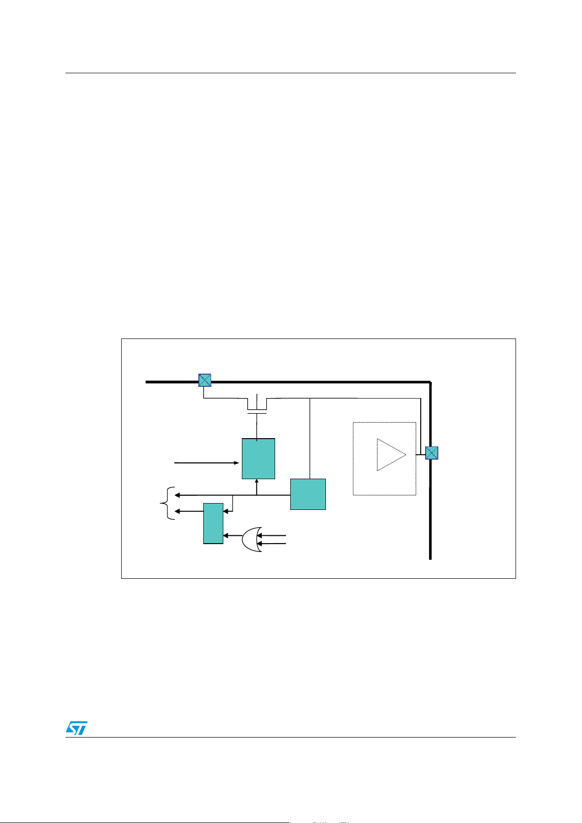
L6460 Low voltage power switches
18 Low voltage power switches
Low voltage power switches are analog switches designed to operate from a single +2.4 V
to +3.6 V V
GPIO_SPI
voltage devices. When switched on, they connect the V
(GPIO[6] for low voltage power switch 1 or GPIO[7] for low voltage power switch 2) thus
powering the device connected to it. The turning on and off of each switch can be controlled
through serial interface.
L6460 provides 2 low voltage power switches, each of them has current limitation to
minimum 150mA to limit inrush current when charging a capacitive load. When the limit
current has been reached, for more than a T
latched in the central logic and can be cleared by the firmware. Please note that, in case of
capacitive load, the current limit is reached the first time the low power switch is turned on:
therefore the user will find a limit flag that must be cleared.
The 2 low voltage power switches can be externally paralleled to obtain a single super low
voltage power switch. Low voltage pass switches sink current needed for their functionality
from pin V
GPIO_SPI
Figure 27. Low power switch block diagram
supply. They are intended to provide and remove power supply to low
GPIO_SPI
time, then a flag is activated; this flag is
filter
pin to their output pin
, they never inject current on this pin.
V
GPIO_SPI
EnLowVSw[x]
GPIO[6] (LPS 1)
or
Circuit
Driving
To SPI
LowVSwIlim[x]
S
LowVSwIlimLth[x]
R
ClrLowVrSwLth
Current
Limit
Sensor
Reset State
GPIO[6]/GPIO[7]
Driver
GPIO[7] (LPS 2)
Doc ID 17713 Rev 1 89/139

General purpose PWM L6460
19 General purpose PWM
L6460 includes three general purpose PWM generators that can be redirected on GPIO
pins (see Chapter 22). Two of these generators (Aux_PWM_1 and Aux_PWM_2) work with
a fixed period F
has a programmable base time clock and a programmable time for both high and low levels.
19.1 General purpose PWM generators 1 and 2 (AuxPwm1 and AuxPwm2)
The Duty cycle of these PWM generators can be changed by writing the AuxPwmXCtrl bits
(where X can be 1 or 2) in the AuxPwm1Ctrl and AuxPwm2Ctrl registers. Their positive duty
cycle will change according to the equation:
According to this equation a programmed “0” value will cause a 0% duty cycle (output
always at logic level 0).
/512 and have a programmable duty cycle; the other one (GP_PWM)
OSC
PWM_X_DUTY AuxPwmXCtrl 9:0[]/512=
19.2 Programmable PWM generator (GpPwm)
GpPWM has a programmable base clock that can be changed by programming the
GpPwmBase[6:0] bits in the GpPwmBase register. The clock will change according to the
equation:
PWM_BASE_PERIOD GpPwmBase 6:0[]1+()Tosc×=
The high and low level duration (expressed in base clock periods), can be programmed
writing the GpPwmHigh[7:0] and GpPwmLow[7:0] bits in the GpPwmCtrl register so they will
change according to following equations:
High_level_Time GpPwmHigh 7:0[]PWM_BASE_PERIOD×=
Low_level_Time GpPwmLow 7:0[]PWM_BASE_PERIOD×=
The resulting period of the PWM will be:
Period GpPwmHigh 7:0[]GpPwmLow 7:0[]+()PWM_BASE_PERIOD+=
and the positive duty cycle will result:
DutyCycle
---------------------------------------------------------------------------------------------- High_level_Time Low_level_Time+
A programmed value of 0 in GpPwmHigh[7:0] and GpPwmLow[7:0] bits will force the PWM
generator output to be always at logic level “0”.
High_level_Time
-------------------------------------------------------------------------------------------------------- -==
GpPwmHigh 7:0[]GpPwmLow 7:0[]+
GpPwmHigh 7:0[]
90/139 Doc ID 17713 Rev 1

L6460 Interrupt controller
20 Interrupt controller
L6460 contains one programmable interrupt controller that can be used to advice the
firmware, through the serial interface, when a certain event happens inside the IC. The
output of the interrupt circuit can be also redirected on a GPIO pin therefore the event can
be signaled directly to the external circuits.
Figure 28. Interrupt controller diagram
IntCtrlAutoDisab
EnIntCtrlPulse
le
DisableMonitor
Disable Pulse
DisableSignals
Generation
logic
Monitored signals
Enable signals
EnIntCtrl
Decode logic
IntCtrlPolarity
Pulse
Generator
EnIntCtrlPulse
The Ta bl e 3 6 contains the events that can be monitored by the interrupt controller.
Table 36. Interrupt controller event
Event Event description Notes
To Gpio
Mtr1Fault Bridge 1 fault (Ilimit event)
Mtr2Fault Bridge 2 fault (Ilimit event)
Mtr3Fault Bridge 3 fault (Ilimit event)
Mtr4Fault Bridge 4 fault (Ilimit event)
nAWAKE nAWAKE pin low
SwRegCtrl Ilimit Switching regulator controller Ilimit event.
VMainSW Ilimit Main switching regulator Ilimit event.
LowPowSw 1 Low voltage power switch 1 Ilimit event.
LowPowSw 2 Low voltage power switch 2 Ilimit event
Warm Warming event
Doc ID 17713 Rev 1 91/139

Interrupt controller L6460
Table 36. Interrupt controller event (continued)
Event Event description Notes
WDWarn Watch dog warning event
WD Watch dog event
DigCmp Digital comparator
ADCDone1 ADC conversion done 1
ADCDone2 ADC conversion done 2
(1)
(1)
Vloop1Ilim AUX1 Ilimit event.
1. This event is disabled if the related ADC channel is configured in continuous mode.
Any event detection can be enabled and disabled by setting at logic level 1 the relative
enable bit in the interrupt controller configuration register (IntCrtlCfg).
The interrupt controller can be programmed to give a pulse when a monitored event
happens or to continuously maintaining the output active until the interrupt condition is
finished.
When programmed to signal the enabled events by giving pulses, the interrupt controller can
be configured to disable the event that caused the interrupt request until the firmware reenables it writing the relative bit in the control register (IntCrtlCtrl) or to continue to monitor
the event.
The GPIO output of this circuit can be programmed to be active high or active low.
92/139 Doc ID 17713 Rev 1

L6460 Digital comparator
21 Digital comparator
L6460 includes one digital comparator that can be used to signal, through serial interface,
that a channel converted by the ADC is greater, greater-equal, lesser, lesser equal, or equal
than a fixed value set by serial interface or than the value converted by the other ADC
channel.
This circuit can be used to monitor the temperature of the IC advising the firmware when it
reaches a certain value decided by the firmware by setting one ADC channel to do
continuous conversions of the temperature sensor.
The circuit operation can be enabled or disabled changing the EnDigCmp bit in the
configuration register DigCmpCfg. By setting the DigCmpUpdate[1:0] bits in the
configuration register, the comparator can be programmed to update its output in one of the
following ways:
● DigCmpUpdate[1:0]=00
– Continuously (each clock).
● DigCmpUpdate[1:0]=01
– Each time a conversion is performed on ADC channel 0.
● DigCmpUpdate[1:0]=10
– Each time a conversion is performed on ADC channel 1.
● DigCmpUpdate[1:0]=11
– ADC state machine driven.
When the last option is selected, the digital comparator will update its output in two different
ways depending on the configuration of the ADC converter. If ADC converter is configured to
do continuous conversions on both channels, the output of the comparator will be updated
when the double conversion is completed. If ADC converter is not configured to do
continuous conversions on both channels, the output of the comparator will be updated each
time a conversion is completed.
The comparator output can be digitally filtered so that the programmed condition has to be
found for three consecutive checks before to be signaled.
The Figure 29 shows the block diagram of digital comparator.
Doc ID 17713 Rev 1 93/139
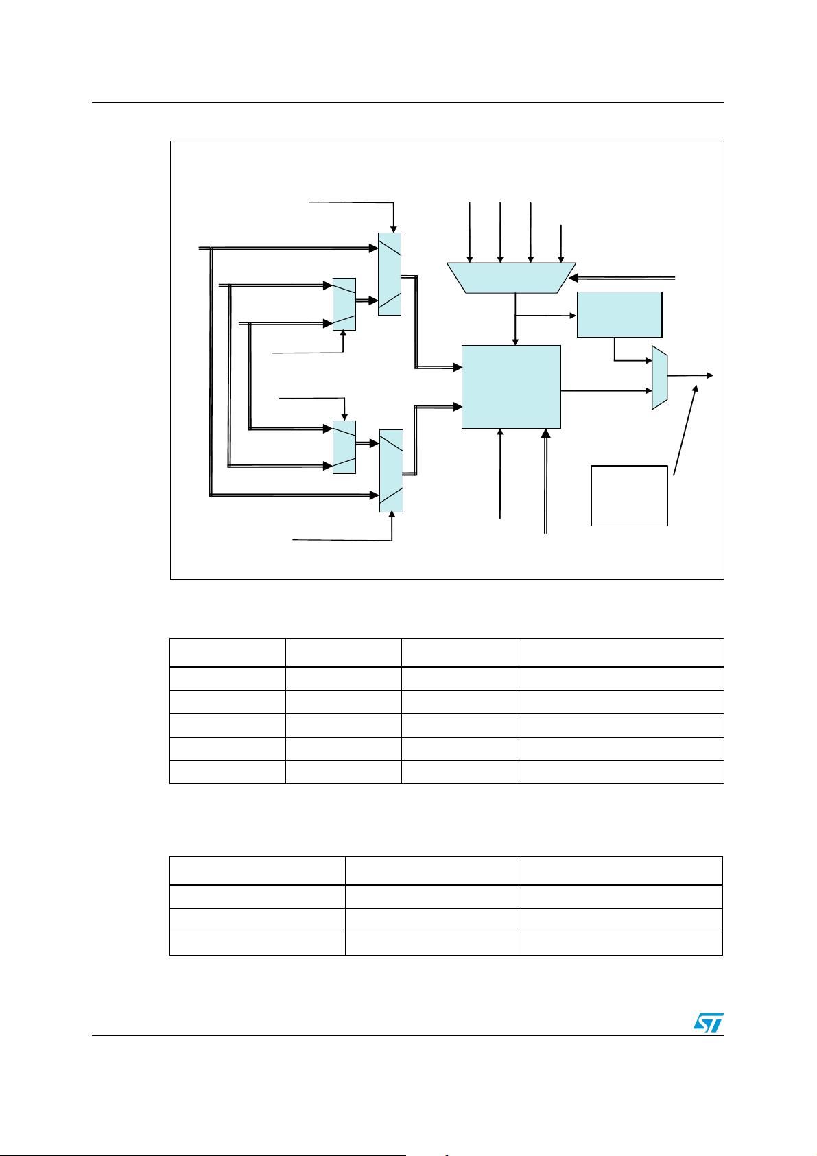
Digital comparator L6460
Figure 29. Digital comparator block diagram
DigCmpValue[9:0]
A2DResult0[8:0]
A2DResult1[8:0]
DigCmpSelCh0[0]
DigCmpSelCh1[0]
DigCmpSelCh0[1]
DigCmpSelCh1[1]
Data0[9:0]
Data1[9:0]
A2DDone0
Logic ‘1’
COMPARATOR
EnDigCmp
ADC FSM
Update
Signal
A2DDone1
DigCmpUpdate[1:0]
Three checks
filter
CmpOut
SelCmpType[1:0 ]
In Ta bl e 3 7 is reported the comparison type truth table.
Table 37. Comparison type truth table
EnDigCmp SelCmpType[1] SelCmpType[0] Comparison type
0 X X Disabled
1 0 0 Data0[9:0] ≤1³1÷Data1[9:0]
1 0 1 Data0[9:0] = Data1[9:0]
1 1 0 Data0[9:0] > Data1[9:0]
1 1 1 Data0[9:0] ≤= Data1[9:0]
In Ta bl e 3 8 is reported the Data0/Data1 selection truth table.
Table 38. DataX selection truth table
DigCmpSelChX[1] DigCmpSelChX[0] DataX[9:0]
0 X DigCmpValue[9:0]
1 0 A2DResult1[8:0]
1 1 A2DResult1[8:0]
94/139 Doc ID 17713 Rev 1

L6460 GPIO pins
22 GPIO pins
Some of the pins of L6460 are indicated as GPIO (General purpose I/O). These pins can be
configured to be used in different ways depending on customer application. All GPIOs can
be used as digital input/output pins with digital value settable/readable using serial interface
or as analog input pins that can be converted using the A2D system. Some of the pins can
be used for special purposes: i.e. two of them can be used to access to the pass switch
function, other two are used as feedback pins for the auxiliary synchronous switching
regulators.
All input Schmitt triggers and output circuitry used for start-up purposes are powered by the
internally generated V
ensure independency between V
driver or the high side MOS is in back-to-back configuration to avoid the presence of the
body diode between output and supply.
All digital output signals can be inverted before being provided on the relative GPIO pins.
Here below is reported the table with GPIO functions.
Table 39. GPIO functions description
Pin
Name
Analog Digital Analog Digital
, while the digital output buffers are powered by V
3v3
and V
3v3
Function
GPIO_SPI
(1)
the GPIOs output drivers are open-drain
Special
GPIO_SPI
NotesInput Output
pin. To
- SPI OUT
Start-up
configuration
pin
Open drain
output
GPIO[0] - ADC input - SPI IN
- Interrupt ctrl.
- AuxPwm1
- AuxPwm2
- ADC input
GPIO[1]
- Comp1 In-
- SPI IN
- Vaux1 F.B.
GPIO[2]
- ADC input
- Comp2 In-
- Vaux2 F.B.
- SPI IN
- IN PWM
GPIO[3] - ADC input - SPI IN
GPIO[4] - ADC input - SPI IN
GPIO[5] - ADC input - SPI IN
- SPI OUT
- Interrupt ctrl.
- AuxPwm1
- AuxPwm2
- SPI OUT
- Interrupt ctrl.
- AuxPwm2
- AuxPwm3
- SPI OUT
- AuxPwm2
- AuxGpPwm3
- SPI OUT
- Interrupt ctrl.
- AuxPwm1
- AuxPwm3
- SPI OUT
- Reg. loop 1
- Comp1 out
- AuxPwm3
Start-up
configuration
pin
Start-up
configuration
pin
Slave Control
Open drain
output
Open drain
output
Open drain
output
Open drain
output
Full driver BB
powered by
V
3v3
Doc ID 17713 Rev 1 95/139

GPIO pins L6460
Table 39. GPIO functions description (continued)
Function
Pin
Name
Analog Digital Analog Digital
(1)
NotesInput Output
Special
GPIO[6] - ADC input - SPI IN - Low Pow Sw 1
GPIO[7] - ADC input - SPI IN - Low Pow Sw 2
GPIO[8] - ADC input - SPI IN
GPIO[9]
GPIO[10]
- ADC input
- OpAmp1 in+
- ADC input
- OpAmp1 in-
GPIO[11] - ADC input
- SPI IN
- ID 1
- IN PWM
- SPI IN
- ID 2
- IN PWM
- SPI IN
- IN PWM
(2)
- CurrDAC
- OpAmp1 Out
- SPI OUT
- A2DGpo
- AuxPwm2
- Comp2 out
- SPI OUT
- AuxPwm1
- AuxPwm3
- Comp1 out
- SPI OUT
- AuxPwm1
- AuxPwm3
- Comp2 out
- SPI OUT
- Interrupt contr.
- AuxPwm1
- Reg. loop 3
- SPI OUT
- Interrupt ctrl.
- AuxPwm2
- AuxPwm3
- SPI OUT
- A2DGpo
- AuxPwm1
- AuxPwm2
5 volt input
tolerant
Full driver
connected to
V
GPIO_SPI
Full driver
connected to
V
GPIO_SPI
Open drain
output
Full driver
connected to
V
GPIO_SPI
Full driver
connected to
V
GPIO_SPI
Full driver
connected to
V
GPIO_SPI
- SPI OUT
GPIO[12]
- ADC input
- OpAmp2 in+
- SPI IN
- STEP_REQ
- Interrupt ctrl
- Comp2 out
- Reg. loop 2
- SPI OUT
GPIO[13]
- ADC input
- OpAmp2 in-
- SPI IN
- AuxPwm1
- Reg. loop 3
- AuxPwm3
- SPI OUT
GPIO[14] - ADC input - SPI IN - OpAmp2 Out
1. In this table are used the abbreviations of the following In Table 40.
2. GPIO[8] input Schmitt trigger is disabled by default (after a reset) to be able to read the digital value from this pin it needs
to be enabled writing a logic ‘1’ in the EnGpio8DigIn in CurrDacCtrl register.
- Interrupt ctrl.
- AuxPwm2
- AuxPwm3
96/139 Doc ID 17713 Rev 1
Full driver BB
(can be
powered by
with a
V
3v3
metal change)
Full driver
connected to
V
GPIO_SPI
Full driver
connected to
V
GPIO_SPI

L6460 GPIO pins
Table 40. Abbreviations
Abbreviation Meaning
ADC input Input to the ADC system.
SPI IN Digital state of this pin is readable through SPI.
SPI OUT Digital state of this pin can be set through SPI.
BB Back to back high side driver.
Comp1 IN - This pin can be used as minus input for comparator 1.
Comp2 IN - This pin can be used as minus input for comparator 2.
Vaux1 FB
A2DGpo
Reg. Loop 3
This pin can be used as feedback input for AUX1 regulator obtained by
using bridge 3.
This pin can be used to carry out the A2DGpo value related to the ADC
conversion
L6460 is doing.
This pin can be used as output of the regulation loop used by AUX3
regulator obtained by using bridge 4.
STEP_REQ This pin can be used to request a stepper sequencer evolution step.
Interrupt Ctrl This pin can be used to carry out the interrupt controller circuit output.
Vaux2 FB
This pin can be used as feedback pin by AUX2 regulator obtained by using
bridge 3
IN PWM This pin can be used to provide an external PWM to bridges.
Reg. Loop 1
This pin can be used as output of the regulation loop used by AUX1
regulator.
Comp1 OUT This pin can be used as output of the comparator 1.
AuxPwm1 This pin can be used to carry out the PWM generated by AuxPwm1 circuit.
Low Volt. Pow. Sw. 1 This pin can be used as output of low voltage power switch 1.
Reg. Loop 2
This pin can be used as output of the regulation loop used by AUX2
regulator.
Comp2 OUT This pin can be used as output of the comparator 2.
AuxPwm2 This pin can be used to carry out the PWM generated by AuxPwm2 circuit.
Low Volt. Pow. Sw. 2 This pin can be used as output of low voltage power switch 2.
Reg. Loop 3
This pin can be used as output of the regulation loop used by AUX3
regulator.
AuxPwm3 This pin can be used to carry out the PWM generated by AuxPwm3 circuit.
CurrDAC This pin can be used to carry out the output of the current DAC circuit.
AuxPwm4 This pin can be used to carry out the PWM generated by AuxPwm4 circuit.
OpAmp1 in+ This pin can be used as operational amplifier 1 non-inverting input.
OpAmp1 in- This pin can be used as operational amplifier 1 inverting input.
OpAmp1 Out This pin can be used as operational amplifier 1 output.
OpAmp2 in+ This pin can be used as operational amplifier 2 non-inverting input.
OpAmp2 in- This pin can be used as operational amplifier 2 inverting input.
Doc ID 17713 Rev 1 97/139

GPIO pins L6460
Table 40. Abbreviations (continued)
Abbreviation Meaning
OpAmp2 Out This pin can be used as operational amplifier 2 output.
ID 1 This pin is used to determine the SPI ID1 bit value.
ID 2 This pin is used to determine the SPI ID2 bit value.
Slave Control This pin is used as slave control when the IC is configured as master.
Hereafter are reported the detailed specifications for each GPIO.
To enable the functionality of the GPIO as output pin, the relative GpioOutEnable[14:0] bit
must be enabled in GpioOutEnable register.
Each GPIO could be configured by setting the appropriate GpioXMode[2:0] in the GpioCtrlX
register.
98/139 Doc ID 17713 Rev 1

L6460 GPIO pins
22.1 GPIO[0]
The GPIO[0] truth table is (for the abbreviation list please refer to Tabl e 4 0 ).
Table 41. GPIO[0] truth table
GPIO[0] SPI BITS
State at
StartUp
GpioOut
Enable [0]
Mode[2] Mode[1] Mode[0]
Function Note
1 X X X X Detection of StartUp config
0 0 X X X HiZ (SPI_IN)
0 1 0 0 0 SPI OUT
0 1 0 0 1 InterruptCtrl
01 0 1 0 AuxPwm1
01 0 1 1 AuxPwm2
0 1 1 0 0 SPI OUT inverted
0 1 1 0 1 InterruptCtrl inverted
0 1 1 1 0 AuxPwm1 inverted
0 1 1 1 1 AuxPwm2 inverted
1. In all configurations in which GPIO[0] is enabled as output:
a) the GPIO[0] pin can be always used as an analog input to the ADC system (ADC function) by writing its
address in the A2DChannelX[4:0] in the A2DConfigX register and starting a conversion;
b) the GPIO[0] pin can be always used as a digital input so its value can be always read through SPI
interface (SPI_IN function);
c) the GPIO[0] pin is an open drain output.
See
Chapter 8
(1)
(1)
(1)
(1)
(1)
(1)
(1)
(1)
Doc ID 17713 Rev 1 99/139

GPIO pins L6460
Figure 30. GPIO[0] block diagram
V
3v3
To Serial Interface
To ADC
V
3v3
To Control Logic
From Serial
Interface
EnStartUpDtc
V
3v3
Logic Decode
Start-up pin State
Detect circuit
V
3v3
GPIO[0] Driver
GPIO[0]
From Power Up
FSM
100/139 Doc ID 17713 Rev 1
 Loading...