

Page 1
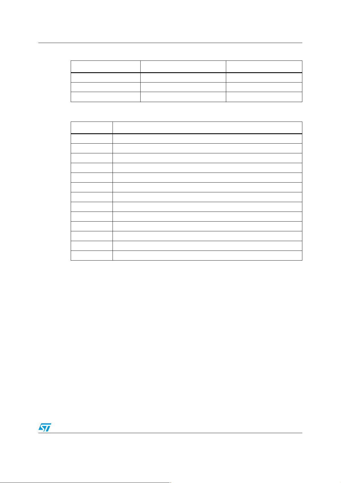
L6221
Quad Darlington switch
Features
■ Four non-inverting inputs with enable
■ Output voltage up to 50 V
■ Output current up to 1.8 A
■ Very low saturation voltage
■ TTL compatible inputs
■ Integral fast recirculation diodes
Applications
The L6221 monolithic quad Darlington switch is
designed for high current, high voltage switching
applications.
Description
Each of the four switches is controlled by a logic
input and all four are controlled by a common
enable input. All inputs are TTL-compatible for
direct connection to logic circuits.
Each switch consists of an open-collector
Darlington transistor plus a fast diode for
switching applications with inductive device loads.
The emitters of the four switches are commoned.
Any number of inputs and outputs of the same
device may be paralleled.
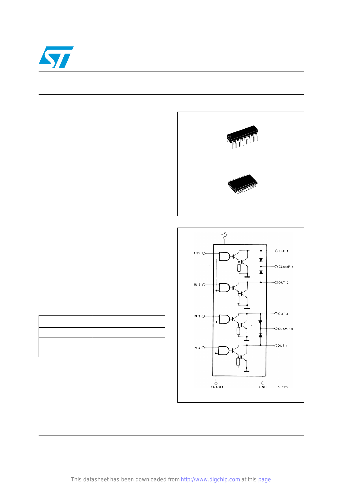
Table 1. Device summary
Power DIP 12+2+2
SO16+2+2
Figure 1. Block diagram
Order code Package
E-L6221AS Power DIP
E-L6221AD SO16+2+2
E-L6221AD013TR SO16+2+2 (tape and reel)
January 2009 Rev 3 1/22
www.st.com
This datasheet has been downloaded fromhttp://www.digchip.com at this page
22
Page 2

Contents
Contents
1 Thermal data . . . . . . . . . . . . . . . . . . . . . . . . . . . . . . . . . . . . . . . . . . . . . . . 3
2 Pin information . . . . . . . . . . . . . . . . . . . . . . . . . . . . . . . . . . . . . . . . . . . . . 4
3 Absolute maximum ratings . . . . . . . . . . . . . . . . . . . . . . . . . . . . . . . . . . . 6
4 Electrical characteristics . . . . . . . . . . . . . . . . . . . . . . . . . . . . . . . . . . . . . 7
5 Test circuits . . . . . . . . . . . . . . . . . . . . . . . . . . . . . . . . . . . . . . . . . . . . . . . . 8
6 Application information . . . . . . . . . . . . . . . . . . . . . . . . . . . . . . . . . . . . . 14
7 Mounting instructions . . . . . . . . . . . . . . . . . . . . . . . . . . . . . . . . . . . . . . . 16
8 Package mechanical data . . . . . . . . . . . . . . . . . . . . . . . . . . . . . . . . . . . . 18
9 Revision history . . . . . . . . . . . . . . . . . . . . . . . . . . . . . . . . . . . . . . . . . . . 21
2/22
Page 3

Thermal data
1 Thermal data
Table 2. Thermal data
Symbol Parameter SO20 Power DIP Unit
R
th j-pins
R
th j-amb
Thermal resistance junction-pins max. 17 14 °C/W
Thermal resistance junction-ambient max. 80 80 °C/W
3/22
Page 4

Pin information
2 Pin information
Figure 2. Pin connections (top views)
E-L6221AS (Power DIP)
E-L6221AD (SO16+2+2)
4/22
Page 5
Pin information
Table 3 . Truth t able
(1)
Enable Input Power out
HH ON
HLOFF
LXOFF
1. For each input: H = High level, L = Low level
Table 4. Pin description
(1)
Name Function
IN 1 Input to driver 1
IN 2 Input to driver 2
OUT 1 Output of driver 1
OUT 2 Output of driver 2
CLAMP A Diode clamp to driver 1 and driver 2
IN 3 Input to driver 3
IN 4 Input to driver 4
OUT 3 Output of driver 3
OUT 4 Output of driver 4
CLAMP B Diode clamp to driver 3 and driver 4
ENABLE Enable input to all drivers
V
S Logic supply voltage
GND Common ground
1. See
Figure 1: Block diagram
5/22
Page 6
Absolute maximum ratings
3 Absolute maximum ratings
Table 5. Absolute maximum ratings
Symbol Parameter Value Unit
V
o
V
s
VIN, V
I
C
I
C
I
C
T
op
T
stg
I
sub
P
tot
Output voltage 50 V
Logic supply voltage 7 V
Input voltage, enable voltage V
EN
Continuous collector current (for each channel) 1.8 A
Collector peak current (repetitive, duty cycle = 10% ton = 5 ms) 2.5 A
Collector peak current (non repetitive, t = 10 μ s) 3.2 A
Operating temperature range (junction) -40 to +150 °C
Storage temperature range -55 to +150 °C
Output substrate current 350 mA
Total power dissipation at:
T
= 90 ° C (Power DIP)
pins
T
= 90°C (SO20)
case
T
= 70 ° C (Power DIP)
amb
T
= 70°C (SO20)
amb
4.3
3.5
1
1
S
W
W
W
W
6/22
Page 7
Electrical characteristics
4 Electrical characteristics
Note: Refer to the test circuits Figure 3 to Figure 10 (VS = 5 V, T
= 25 °C unless otherwise
amb
specified).
Table 6. Electrical characteristics
Symbol Parameter Test condition Min. Typ. Max. Unit
V
S
I
s
V
CE(sus)
I
CEX
V
CE(sat)
VINL, VENL Input low voltage - - - 0.8 V
I
L, IENL Input low current VIN = V
IN
V
L, VENH Input high voltage - 2.0 - - V
IN
IINH, IENH Input high current VIN = VINH, VEN = VENH--10μA
Logic supply voltage - 4.5 - 5.5 V
Logic supply current
All outputs ON, I
= 0.7A - - 20 mA
C
All outputs OFF - - 20 mA
= VINL, VEN = VENH
V
Output sustaining voltage
Output leakage current
Collector emitter saturation
voltage (one input on, all others
inputs off.)
IN
I
= 100 mA
C
VCE = 50V
V
= VINL, VEN = VENH
IN
= 4.5 V
V
s
V
= VINH, VEN = VENH
IN
IC = 0.6 A
IC = 1 A
I
= 1.8 A
C
, VEN = V
INL
ENL
46 - - V
--1mA
-
-
-
-
-
-
1
1.2
1.6
---100 μA
V
I
R
V
F
t
d (on)
t
d (off)
ΔI
Clamp diode leakage current
Clamp diode forward voltage
VR = 50 V, VEN = VENH
VIN = VINL
IF = 1A
IF = 1.8A
- - 100 μA
-
-
-
1.6
-
2.0VV
Tu r n- o n d e l a y t i m e Vp = 5V, RL = 10Ω --2μs
Turn-off delay time Vp = 5V, RL = 10Ω --5μs
= 5V, VEN = 5V
V
s
Logic supply current variation
IN
I
= -300 mA for each
out
channe
l
- - 120 mA
7/22
Page 8

Test circuits
5 Test circuits
Note: Pin numbers without parentheses apply to the Power DIP package.
Pin numbers in parentheses are not applicable.
Figure 3. Logic supply current
Set VIN = 4.5 V, VEN = 0.8 V, or VIN = 0.8 V, VEN = 4.5 V, for IS (all outputs off)
Set V
= 2 V, VEN = 2 V, for IS (all outputs on)
IN
Figure 4. Output sustaining voltage
Figure 5. Output leakage current
8/22
Page 9

Test circuits
Figure 6. Collector-emitter saturation voltage
Figure 7. Logic input characteristics
Set S1, S2 open, VIN, VEN = 0.8 V for IIN L, IEN L
, S2 open, VIN, VEN = 2 V for IIN H, IEN H
Set S
1
Set S
, S2 closed, VIN, VEN = 0.8 V for VIN L, VEN L
1
, S2 closed, VIN, VEN = 2 V for VIN H, VEN H
Set S
1
Figure 8. Clamp-diode leakage current
9/22
Page 10

Test circuits
Figure 9. Clamp-diode forward voltage
Figure 10. Switching time test circuit
Figure 11. Switching time waveforms
10/22
Page 11

Test circuits
Figure 12. Allowed peak collector current versus duty cycle for 1, 2, 3 or 4
contemporary working outputs (L6221AS)
Figure 13. Collector saturation voltage versus collector current
Figure 14. Free-wheeling diode forward voltage versus diode current
11/22
Page 12

Test circuits
Figure 15. Collector saturation voltage versus junction temperature at IC = 1 A
Figure 16. Free-wheeling diode forward voltage versus junction temperature
at I
= 1 A
F
Figure 17. Saturation voltage against junction temperature
12/22
Page 13

Test circuits
Figure 18. Free-wheeling diode forward voltage against junction temperature
13/22
Page 14

Application information
6 Application information
When inductive loads are driven by the L6221, a Zener diode in series with the integral freewheeling diodes increases the voltage across which energy stored in the load is discharged
and therefore speeds the current decay (
For reliability it is suggested that the Zener is chosen so that
There are two reasons for this:
● The Zener voltage changes in temperature and current.
● The instantaneous power must be limited to avoid the reverse second breakdown.
Figure 19. Free-wheeling diode connection when driving inductive loads
Figure 19
VpVz35 V<+
).
Care must be taken to ensure that the collectors are placed close together to avoid different
current partitioning at turn-off.
It is suggested to put in parallel channel 1 and 4 and channel 2 and 3 as shown in
for the similar electrical characteristics of the logic section (turn-on and turn-off delay time)
and the power stages (collector saturation voltage, free-wheeling diode forward voltage).
Figure 20
14/22
Page 15
Application information
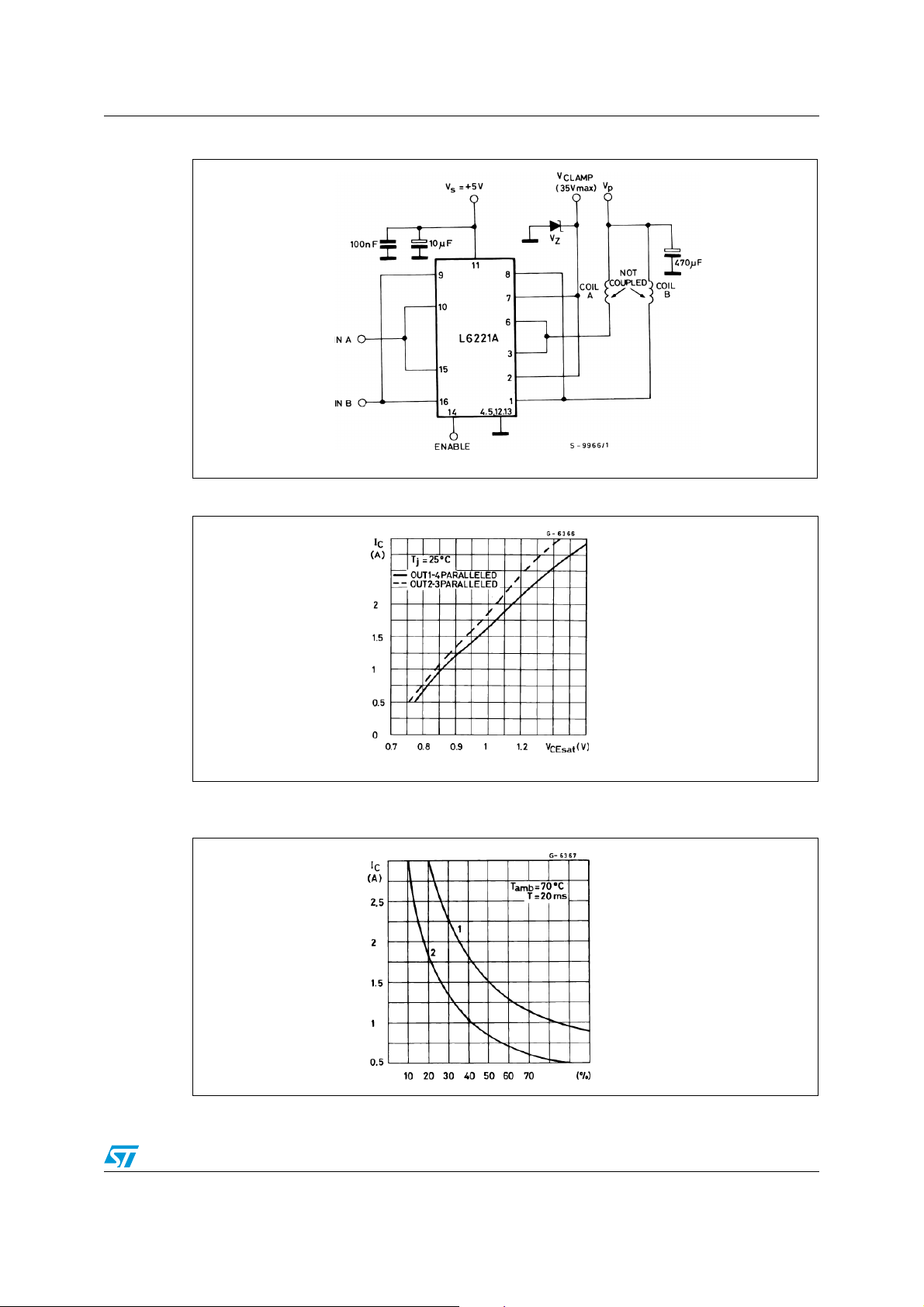
Figure 20. Driver for solenoids up to 3 A
Figure 21. Saturation voltage versus collector current
Figure 22. L6221AS peak collector current versus duty cycle for 1 or 2 paralleled
outputs driven
15/22
Page 16

Mounting instructions
7 Mounting instructions
The R
copper area of the printed circuit board (
Figure 23. Example of PCB copper area used as heat sink
Figure 24. External heat sink mounting example
of the E-L6221AS can be reduced by soldering the GND pins to a suitable
th j-amb
Figure 23
) or to an external heat sink (
Figure 24
).
16/22
Page 17

Mounting instructions
Figure 25
shows the maximum dissipable power P
and the R
tot
as a function of the
th j-amb
side "α" of two equal square copper areas having a thickness of 35 µm (1.4 mils). During
soldering the pins temperature must not exceed 260 °C and the soldering time must not be
longer than 12 seconds.
The external heat sink or printed circuit copper area must be connected to electrical ground.
Figure 25. Maximum dissipable power and junction-to-ambient thermal resistance
versus side "α"
Figure 26. Maximum allowable power dissipation versus ambient temperature
17/22
Page 18

Package mechanical data
8 Package mechanical data
In order to meet environmental requirements, ST offers these devices in different grades of
ECOPACK® packages, depending on their level of environmental compliance. ECOPACK®
specifications, grade definitions and product status are available at:
ECOPACK® is an ST trademark.
www.st.com
.
18/22
Page 19

Package mechanical data
DIM.
a1 0.51 0.020
B 0.85 1.40 0.033 0.055
b 0.50 0.020
b1 0.38 0.50 0.015 0.020
D 20.0 0.787
E 8.80 0.346
e 2.54 0.100
e3 17.78 0.700
F 7.10 0.280
I 5.10 0.201
L 3.30 0.130
Z 1.27 0.050
mm inch
MIN. TYP. MAX. MIN. TYP. MAX.
OUTLINE AND
MECHANICAL DATA
Power DIP 16
Powerdip 16
19/22
Page 20
Package mechanical data
20/22
Page 21

Revision history
9 Revision history
Table 7. Document revision history
Date Revision Changes
14-Jan-2004 2 Released in EDOCS
Document reformatted.
19-Jan-2009 3
Inserted title for
Removed reference to obsolete product L6221N and the associated
package (multiwatt-15).
Figure 19
.
21/22
Page 22

Please Read Carefully:
Information in this document is provided solely in connection with ST products. STMicroelectronics NV and its subsidiaries (“ST”) reserve the
right to make changes, corrections, modifications or improvements, to this document, and the products and services described herein at any
time, without notice.
All ST products are sold pursuant to ST’s terms and conditions of sale.
Purchasers are solely responsible for the choice, selection and use of the ST products and services described herein, and ST assumes no
liability whatsoever relating to the choice, selection or use of the ST products and services described herein.
No license, express or implied, by estoppel or otherwise, to any intellectual property rights is granted under this document. If any part of this
document refers to any third party products or services it shall not be deemed a license grant by ST for the use of such third party products
or services, or any intellectual property contained therein or considered as a warranty covering the use in any manner whatsoever of such
third party products or services or any intellectual property contained therein.
UNLESS OTHERWISE SET FORTH IN ST’S TERMS AND CONDITIONS OF SALE ST DISCLAIMS ANY EXPRESS OR IMPLIED
WARRANTY WITH RESPECT TO THE USE AND/OR SALE OF ST PRODUCTS INCLUDING WITHOUT LIMITATION IMPLIED
WARRANTIES OF MERCHANTABILITY, FITNESS FOR A PARTICULAR PURPOSE (AND THEIR EQUIVALENTS UNDER THE LAWS
OF ANY JURISDICTION), OR INFRINGEMENT OF ANY PATENT, COPYRIGHT OR OTHER INTELLECTUAL PROPERTY RIGHT.
UNLESS EXPRESSLY APPROVED IN WRITING BY AN AUTHORIZED ST REPRESENTATIVE, ST PRODUCTS ARE NOT
RECOMMENDED, AUTHORIZED OR WARRANTED FOR USE IN MILITARY, AIR CRAFT, SPACE, LIFE SAVING, OR LIFE SUSTAINING
APPLICATIONS, NOR IN PRODUCTS OR SYSTEMS WHERE FAILURE OR MALFUNCTION MAY RESULT IN PERSONAL INJURY,
DEATH, OR SEVERE PROPERTY OR ENVIRONMENTAL DAMAGE. ST PRODUCTS WHICH ARE NOT SPECIFIED AS "AUTOMOTIVE
GRADE" MAY ONLY BE USED IN AUTOMOTIVE APPLICATIONS AT USER’S OWN RISK.
Resale of ST products with provisions different from the statements and/or technical features set forth in this document shall immediately void
any warranty granted by ST for the ST product or service described herein and shall not create or extend in any manner whatsoever, any
liability of ST.
ST and the ST logo are trademarks or registered trademarks of ST in various countries.
Information in this document supersedes and replaces all information previously supplied.
The ST logo is a registered trademark of STMicroelectronics. All other names are the property of their respective owners.
© 2009 STMicroelectronics - All rights reserved
STMicroelectronics group of companies
Australia - Belgium - Brazil - Canada - China - Czech Republic - Finland - France - Germany - Hong Kong - India - Israel - Italy - Japan -
Malaysia - Malta - Morocco - Singapore - Spain - Sweden - Switzerland - United Kingdom - United States of America
www.st.com
22/22
 Loading...