

Features
■ Able to drive both windings of bipolar stepper
motor
■ Output current up to 750 mA each winding
■ Wide voltage range: 10 V to 46 V
■ Half-step, full-step and microstepping mode
■ Built-in protection diodes
■ Internal PWM current control
■ Low output saturation voltage
■ Designed for unstabilized motor supply voltage
■ Internal thermal shutdown
Description
L6219
Stepper motor driver
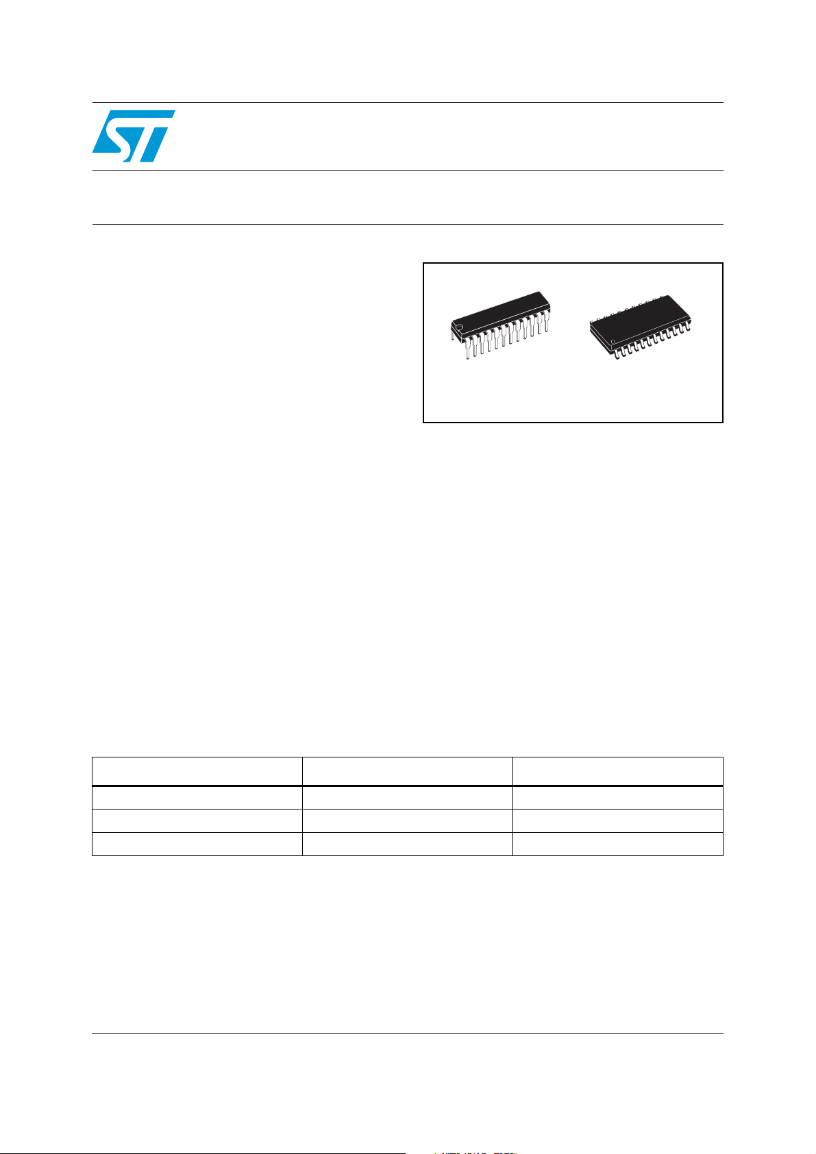
PDIP24 (20+2+2) SO24 (20+2+2)
A cross conduction protection is provided to avoid
simultaneous cross conduction during switching
current direction.
An internal pulse-width-modulation (PWM)
controls the output current to 750 mA with peak
startup current up to 1 A.
The L6219 is a bipolar monolithic integrated
circuits intended to control and drive both winding
of a bipolar stepper motor or bidirectionally control
two DC motors.
The L6219 with a few external components form a
complete control and drive circuit for LS-TTL or
microprocessor controlled stepper motor system.
The power stage is a dual full bridge capable of
sustaining 46V and including four diodes for
current recirculation.
Table 1. Device summary
Part number Package Packing
E-L6219 PDIP24 Tube
E-L6219DS SO24 Tube
E-L6219DS013TR SO24 Tape & reel
Wide range of current control from 750 mA (each
bridge) is permitted by means of two logic inputs
and an external voltage reference. A phase input
to each bridge determines the load current
direction. A thermal protection circuitry disables
the outputs if the chip temperature exceeds safe
operating limits.
September 2008 Rev 13 1/16
www.st.com
1

Contents L6219
Contents
1 Block diagram . . . . . . . . . . . . . . . . . . . . . . . . . . . . . . . . . . . . . . . . . . . . . . 5
2 Functional description . . . . . . . . . . . . . . . . . . . . . . . . . . . . . . . . . . . . . . . 9
2.1 Input logic (I0 and I1) . . . . . . . . . . . . . . . . . . . . . . . . . . . . . . . . . . . . . . . . . 9
2.2 Phase . . . . . . . . . . . . . . . . . . . . . . . . . . . . . . . . . . . . . . . . . . . . . . . . . . . . . 9
2.3 Current sensor . . . . . . . . . . . . . . . . . . . . . . . . . . . . . . . . . . . . . . . . . . . . . . 9
2.4 Single-pulse generator . . . . . . . . . . . . . . . . . . . . . . . . . . . . . . . . . . . . . . . 10
2.5 Output stage . . . . . . . . . . . . . . . . . . . . . . . . . . . . . . . . . . . . . . . . . . . . . . . 10
2.6 VS, VSS, VRef . . . . . . . . . . . . . . . . . . . . . . . . . . . . . . . . . . . . . . . . . . . . . 11
3 Application informations . . . . . . . . . . . . . . . . . . . . . . . . . . . . . . . . . . . . 12
4 Package information . . . . . . . . . . . . . . . . . . . . . . . . . . . . . . . . . . . . . . . . 13
5 Revision history . . . . . . . . . . . . . . . . . . . . . . . . . . . . . . . . . . . . . . . . . . . 15
2/16

L6219 List of tables
List of tables
Table 1. Device summary . . . . . . . . . . . . . . . . . . . . . . . . . . . . . . . . . . . . . . . . . . . . . . . . . . . . . . . . . . 1
Table 2. Absolute maximum rating . . . . . . . . . . . . . . . . . . . . . . . . . . . . . . . . . . . . . . . . . . . . . . . . . . . 5
Table 3. Pin functions . . . . . . . . . . . . . . . . . . . . . . . . . . . . . . . . . . . . . . . . . . . . . . . . . . . . . . . . . . . . . 6
Table 4. Thermal data. . . . . . . . . . . . . . . . . . . . . . . . . . . . . . . . . . . . . . . . . . . . . . . . . . . . . . . . . . . . . 7
Table 5. Electrical characteristcs . . . . . . . . . . . . . . . . . . . . . . . . . . . . . . . . . . . . . . . . . . . . . . . . . . . . 8
Table 6. Current levels . . . . . . . . . . . . . . . . . . . . . . . . . . . . . . . . . . . . . . . . . . . . . . . . . . . . . . . . . . . . 9
Table 7. Document revision history . . . . . . . . . . . . . . . . . . . . . . . . . . . . . . . . . . . . . . . . . . . . . . . . . 15
3/16

List of figures L6219
List of figures
Figure 1. Block diagram . . . . . . . . . . . . . . . . . . . . . . . . . . . . . . . . . . . . . . . . . . . . . . . . . . . . . . . . . . . . 5
Figure 2. SO24/PDIP24 pins connection (top view). . . . . . . . . . . . . . . . . . . . . . . . . . . . . . . . . . . . . . . 6
Figure 3. Timing diagram . . . . . . . . . . . . . . . . . . . . . . . . . . . . . . . . . . . . . . . . . . . . . . . . . . . . . . . . . . . 7
Figure 4. Principle operating sequence . . . . . . . . . . . . . . . . . . . . . . . . . . . . . . . . . . . . . . . . . . . . . . . 10
Figure 5. Typical application circuit . . . . . . . . . . . . . . . . . . . . . . . . . . . . . . . . . . . . . . . . . . . . . . . . . . 12
Figure 6. SO24 mechanical data and package dimensions. . . . . . . . . . . . . . . . . . . . . . . . . . . . . . . . 13
Figure 7. PDIP24 mechanical data and package dimensions . . . . . . . . . . . . . . . . . . . . . . . . . . . . . . 14
4/16
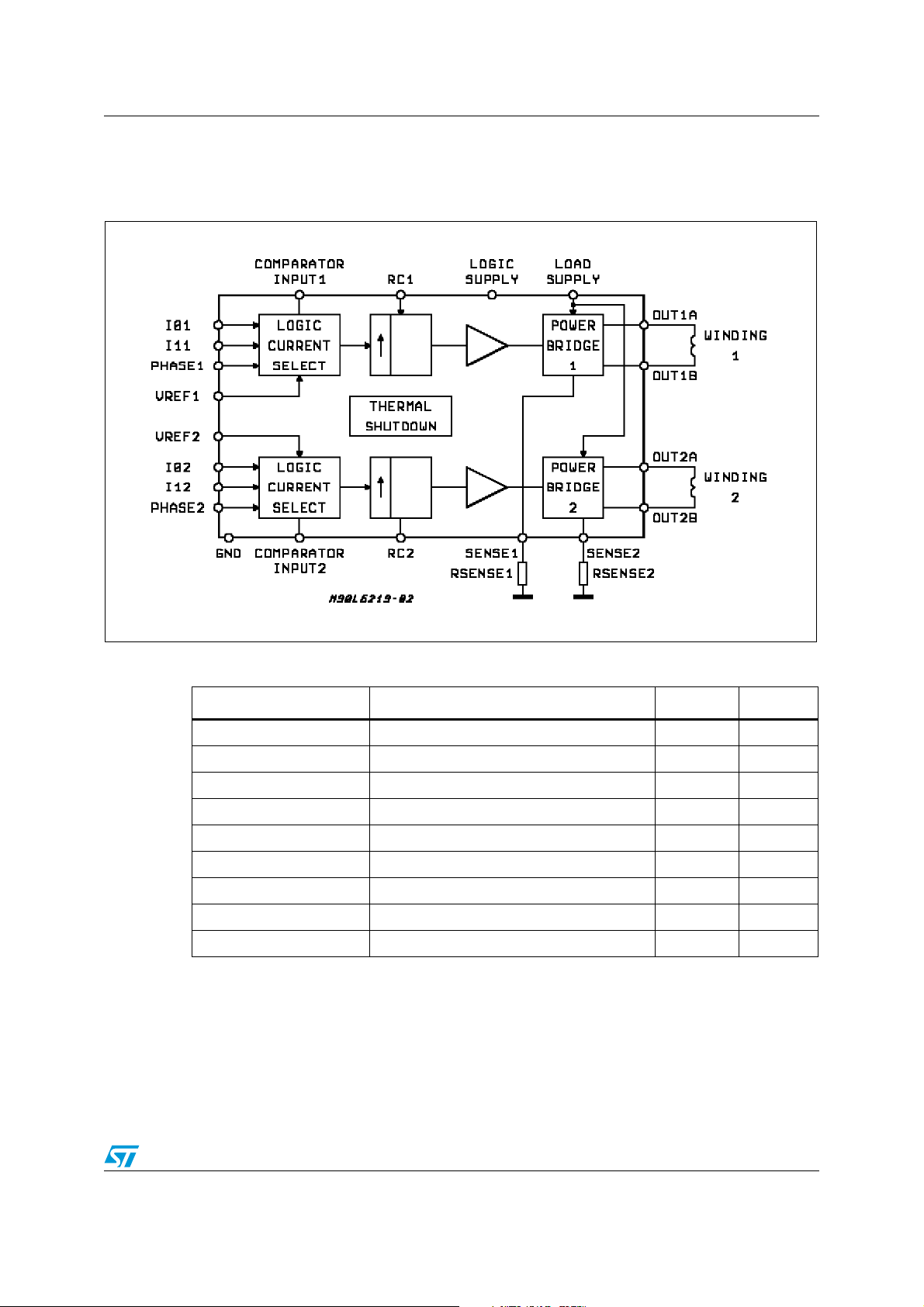
L6219 Block diagram
1 Block diagram
Figure 1. Block diagram
Table 2. Absolute maximum rating
Parameter Description Value Unit
V
T
V
s
I
O
I
O
V
ss
V
in
sense
T
j
T
op
stg
Supply voltage 50 V
Output current (peak) ±1 A
Output current (continuous) ±0.75 A
Logic supply voltage 7 V
Logic input voltage range -0.3 to +7 V
Sense output voltage 1.5 V
Junction temperature +150 °C
Operating temperature range -20 to +85 °C
Storage temperature range -55 to +150 °C
5/16

Block diagram L6219
Figure 2. SO24/PDIP24 pins connection (top view)
Table 3. Pin functions
Pin # Name Description
1, 2 Output A See pins 5, 21
3, 23 Sense resistor
4, 22 Comparator input
5, 21 Output B
6, 19 Ground See pins 7, 18
7, 18 Ground
8, 20 Input 0 See Input 1 (pins 9, 17)
9, 17 Input 1
Connection to lower emitters of output stage for insertion of
current sense resistor
Input connected to the comparators. The voltage across the
sense resistor is feedback to this input throught the low pass
filter RC CC. The higher power transistors are disabled
when the sense voltage exceeds the reference voltage of
the selected comparator. When this occurs the current
decays for a time set by RT CT (toff = 1.1 RT CT). See
Figure 3.
Output connection. The output stage is a H bridge formed
by four transistors and four diodes suitable for switching
applications
Ground connection. With pins 6 and 19 also conducts heat
from die to printed circuit copper
These pins and pins 8, 20 (input 0) are logic inputs which
select the outputs of the comparators to set the current
level. Current also depends on the sensing resistor and
reference voltage. See functional description
6/16

L6219 Block diagram
Table 3. Pin functions (continued)
Pin # Name Description
This TTL-compatible logic inputs sets the direction of
current flow through the load. A high level causes current to
10, 16 Phase
11, 15 Reference voltage
12, 14 RC
flow from output A (source) to output B (sink). A schmitt
trigger on this input provides good noise immunity and a
delay circuit prevents output stage short circuits during
switching
A voltage applied to this pin sets the reference voltage of the
comparators, this determining the output current (also thus
depending on Rs and the two inputs input 0 and input 1)
A parallel RC network connected to this pin sets the OFF
time of the higher power transistors. The pulse generator is
a monostable triggered by the output of the comparators
(toff = 1.1 RT CT)
13 V
24 V
- Logic supply Supply voltage input for logic circuitry
SS
- Load supply Supply voltage input for the output stages
S
Note: ESD on GND, VS, VSS, OUT 1 A and OUT 2 A is guaranteed up to 1.5 KV (human body
model, 1500 W, 100 pF).
Figure 3. Timing diagram
Table 4. Thermal data
Parameter Description PDIP SO Unit
R
thj-case
R
thj-amb
1. With minimized copper area.
Thermal resistance junction-case max. 14 18 °C/W
Thermal resistance junction-ambient max. 60
(1)
75
(1)
°C/W
7/16

Block diagram L6219
Table 5. Electrical characteristcs
(
Tj = 25 °C, VS = 46 V, VSS = 4.75 V to 5.25 V, V
specified
Parameter Description Test condition Min. Typ. Max. Unit
Output drivers (OUTA or OUTB)
V
I
CEX
V
CE(sat)
I
R
V
I
S(on)
I
S(off)
Control logic
V
IN(H)
V
IN(L)
I
IN(H)
I
IN(L)
V
REF
I
SS(ON)
I
SS(OFF)
Comparators
V
/ V
REF
t
off
t
d
Protection
T
1. To reduce the switching losses the base bias of the bridge's low side NPN transistor is proportional to the
DAC output, then the output current driving capability is also proportional to the DAC output voltage, having
as reference 750 mA with V
output maximum current driving capability will become 750 mA*(2V*0.67)/(5V*1) = 200 mA.
Motor supply range 10 46 V
S
Output leakage current
Output saturation voltage
Clamp diode leakage
current
Clamp diode forward
F
voltage
Driver supply current Both bridges ON, no load - 8 15 mA
Driver supply current Both bridges OFF - 6 10 mA
Input voltage All inputs 2.4 - - V
Input voltage All inputs - - 0.8 V
Input current VIN = 2.4 V - <1 20 μA
Input current VIN = 0.84 V - -3 -200 μA
Reference voltage Operating
Total logic supply current Io = I1 = 0.8 V, no load - 64 74 mA
Total logic supply current Io = I1 = 2.4 V, no load - 10 14 mA
Current limit threshold (at
sense
trip point)
Cutoff time Rt = 56 KΩ Ct = 820 pF - 50 μs
Turn off delay Figure 3 -1 μs
Thermal shutdown
J
temperature
)
See Figure 5
= 5 V and DAC =100%. For example using V
REF
V
= Vs,
OUT
V
= 0
OUT
Sink driver, I
Sink driver, I
Source driver, I
Source driver, I
= +500 mA
OUT
= +750 mA
OUT
= -500 mA
OUT
= -750 mA
OUT
= 50 V - <1 50 μA
V
R
Sink diode
Source diode I
I
= I1 = 0.8 V 9.5 10 10.5 -
o
I
= 2.4 V, I1 = 0.8 V 13.5 15 16.5 -
o
I
= 0.8 V, I1 = 2.4 V 25.5 30 34.5 -
o
= 750 mA
F
(1)
= 5 V, unless otherwise
REF
-
<1
-
<-150-50μAμA
-
0.3
-
0.7
-
1.1
-
1.3
1
1
1.5 - 7.5 V
-170-°C
= 2 V and DAC = 67% the
REF
0.6
1
1.4
1.6
1.5
1.5VV
V
V
V
V
8/16

L6219 Functional description
2 Functional description
The circuit is intended to drive both windings of a bipolar stepper motor.
The peak current control is generated through switch mode regulation. There is a choice of
three different current levels with the two logic inputs I01 - I11 for winding 1 and I02 - I12 for
winding 2.
The current can also be switched off completely.
2.1 Input logic (I0 and I1)
The current level in the motor winding is selected with these inputs. (See Figure 4). If any of
the logic inputs is left open, the circuit will treat it has a high level input.
Table 6. Current levels
I0 I1 Current level
H H No current
L H Low current 1/3 IO max
H L Medium current 2/3 IO max
L L Maximum current IO max
2.2 Phase
This input determines the direction of current flow in the windings, depending on the motor
connections. The signal is fed through a schmidt-trigger for noise immunity, and through a
time delay in order to guarantee that no short-circuit occurs in the output stage during
phase-shift. High level on the phase input causes the motor current flow from out A through
the winding to out B.
2.3 Current sensor
This part contains a current sensing resistor (RS), a low pass filter (RC, CC) and three
comparators. Only one comparator is active at a time. It is activated by the input logic
according to the current level chosen with signals I
the sensing resistor RS. When the current has increased so that the voltage across R
becomes higher than the reference voltage on the other comparator input, the comparator
goes high, which triggers the pulse generator.
The max peak current Imax can be defined by:
I
max
and I1. The motor current flows through
o
V
ref
-------------=
10R
s
S
9/16

Functional description L6219
2.4 Single-pulse generator
The pulse generator is a monostable triggered on the positive going edge of the comparator
output. The monostable output is high during the pulse time, toff, which is determined by the
time components Rt and Ct.
t
= 1.1 · RtCt
off
The single pulse switches off the power feed to the motor winding, causing the winding
current to decrease during t
. If a new trigger signal should occur during t
off
, it is ignored.
off
2.5 Output stage
The output stage contains four darlington transistors (source drivers) four saturated
transistors (sink drivers) and eight diodes, connected in two H bridge.
Figure 4. Principle operating sequence
The source transistors are used to switch the power supplied to the motor winding, thus
driving a constant current through the winding. It should be noted however, that is not
permitted to short circuit the outputs.
10/16

L6219 Functional description
Internal circuitry is added in order to increase the accuracy of the motor current particularly
with low current levels.
2.6 VS, VSS, V
The circuit will stand any order of turn-on or turn-off the supply voltages VS and VSS. Normal
dV/dt values are then assumed.
Preferably, V
Ref
Ref
should be tracking VSS during power-on and power-off if VS is established.
11/16
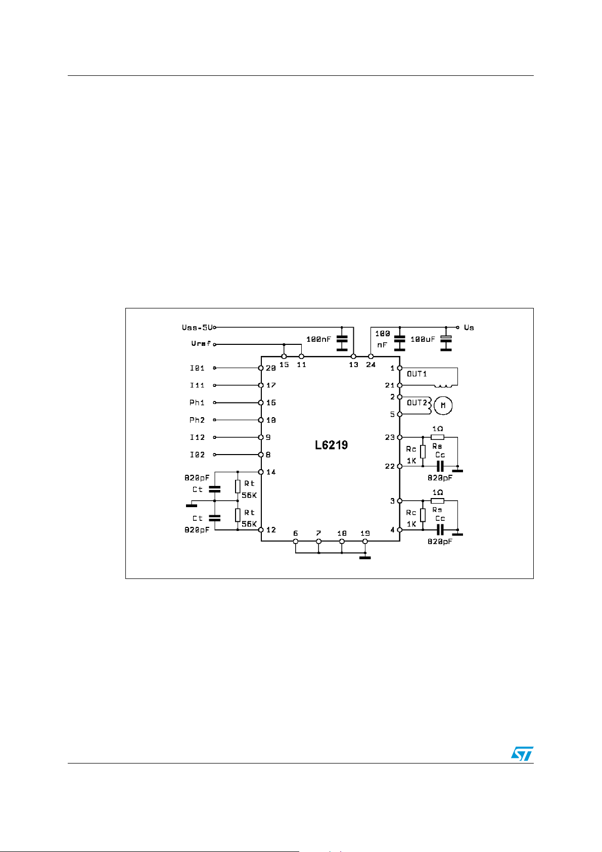
Application informations L6219
3 Application informations
Some stepper motors are not designed for contin-uous operation at maximum current. As
the circuit drives a constant current through the motor, its temperature might increase
exceedingly both at low and high speed operation. Also, some stepper motors have such
high core losses that they are not suited for switch mode current regulation.
Unused inputs should be connected to proper voltage levels in order to get the highest noise
immunity. As the circuit operates with switch mode current regulation, interference
generation problems might arise in some applications. A good measure might then be to
decouple the circuit with a 100 nF capacitor, located near the package between power line
and ground. The ground lead between Rs, and circuit GND should be kept as short as
possible. A typical application circuit is shown in Figure 5. Note that C
similar else. To sense the winding current, paralleled metal film resistors are recommended
(R
).
s
Figure 5. Typical application circuit
must be NPO type or
t
12/16

L6219 Package information
4 Package information
In order to meet environmental requirements, ST offers these devices in ECOPACK®
packages. These packages have a Lead-free second level interconnect. The category of
second Level Interconnect is marked on the package and on the inner box label, in
compliance with JEDEC standard JESD97. The maximum ratings related to soldering
conditions are also marked on the inner box label.
ECOPACK is an ST trademark. ECOPACK specifications are available at: www.st.com.
Figure 6. SO24 mechanical data and package dimensions
DIM.
A 2 .35 2.65 0.093 0.104
A1 0.10 0.30 0.004 0.0 12
B 0 .33 0.51 0.013 0.200
C 0.23 0.32 0.009 0.013
(1)
D
E 7 .40 7.60 0.291 0.299
e 1.27 0.050
H 10.0 10.65 0.394 0.419
h 0.25 0.75 0.010 0.030
L 0.40 1.27 0.016 0.050
k 0˚ (min.), 8˚ (max.)
ddd 0.10 0.004
(1) “D” dimension does not include mold flash, protusions or gate
burrs. Mold f lash, protus ions or gate b urrs shall no t exceed
0.15mm per side.
mm inch
MIN. TYP. MAX. MIN. TYP. MAX.
15.20 15.6 0 0.598 0.614
OUTLINE AND
MECHANICAL DATA
Weight: 0.60gr
SO24
0070769 C
13/16

Package information L6219
Figure 7. PDIP24 mechanical data and package dimensions
DIM.
A 4.320 0.170
A1 0.380 0.015
A2 3.300 0.130
B 0.410 0.460 0.510 0.016 0.018 0.020
B1 1.400 1.520 1.650 0.055 0.060 0.065
c 0.200 0.250 0.300 0.008 0.010 0.012
D 31.62 31.75 31.88 1.245 1.250 1.255
E 7.620 8.260 0.300 0.325
e 2.54 0.100
E1 6.350 6.600 6.860 0.250 0.260 0.270
e1 7.620
L 3.180 3.430 0.125 0.135
M 0˚ min, 15˚ max.
mm inch
MIN. TYP. MAX. MIN. TYP. MAX.
0.300
OUTLINE AND
MECHANICAL DATA
PDIP 24 (0.300")
E1
L
B eB1
24
1
A2
A
A1
e1
D
13
c
12
SDIP24L
M
0034965 D
14/16

L6219 Revision history
5 Revision history
Table 7. Document revision history
Date Revision Changes
30-Oct-2001 7 First Issue on the EDOCS DMS.
11-May-2005 8
Changed the look & feel layout.
Modified Table 6 on page 9.
Change in the Features sections:
14-Sep-2005 9
Wide voltage range 10 V to 46 V
Output current up to 750 mA each winding.
19-Dec-2005 10
28-Mar-2006 11 Corrected I
Corrected in the Tab l e 5 the max. value of the V
V to 7.5 V.
values in the Tab l e 5.
SS(ON)
18-Mar-2008 12 Document reformatted.
01-Sep-2008 13 Added note 1 in Table 5 on page 8.
parameter from 2
REF
15/16

L6219
Please Read Carefully:
Information in this document is provided solely in connection with ST products. STMicroelectronics NV and its subsidiaries (“ST”) reserve the
right to make changes, corrections, modifications or improvements, to this document, and the products and services described herein at any
time, without notice.
All ST products are sold pursuant to ST’s terms and conditions of sale.
Purchasers are solely responsible for the choice, selection and use of the ST products and services described herein, and ST assumes no
liability whatsoever relating to the choice, selection or use of the ST products and services described herein.
No license, express or implied, by estoppel or otherwise, to any intellectual property rights is granted under this document. If any part of this
document refers to any third party products or services it shall not be deemed a license grant by ST for the use of such third party products
or services, or any intellectual property contained therein or considered as a warranty covering the use in any manner whatsoever of such
third party products or services or any intellectual property contained therein.
UNLESS OTHERWISE SET FORTH IN ST’S TERMS AND CONDITIONS OF SALE ST DISCLAIMS ANY EXPRESS OR IMPLIED
WARRANTY WITH RESPECT TO THE USE AND/OR SALE OF ST PRODUCTS INCLUDING WITHOUT LIMITATION IMPLIED
WARRANTIES OF MERCHANTABILITY, FITNESS FOR A PARTICULAR PURPOSE (AND THEIR EQUIVALENTS UNDER THE LAWS
OF ANY JURISDICTION), OR INFRINGEMENT OF ANY PATENT, COPYRIGHT OR OTHER INTELLECTUAL PROPERTY RIGHT.
UNLESS EXPRESSLY APPROVED IN WRITING BY AN AUTHORIZED ST REPRESENTATIVE, ST PRODUCTS ARE NOT
RECOMMENDED, AUTHORIZED OR WARRANTED FOR USE IN MILITARY, AIR CRAFT, SPACE, LIFE SAVING, OR LIFE SUSTAINING
APPLICATIONS, NOR IN PRODUCTS OR SYSTEMS WHERE FAILURE OR MALFUNCTION MAY RESULT IN PERSONAL INJURY,
DEATH, OR SEVERE PROPERTY OR ENVIRONMENTAL DAMAGE. ST PRODUCTS WHICH ARE NOT SPECIFIED AS "AUTOMOTIVE
GRADE" MAY ONLY BE USED IN AUTOMOTIVE APPLICATIONS AT USER’S OWN RISK.
Resale of ST products with provisions different from the statements and/or technical features set forth in this document shall immediately void
any warranty granted by ST for the ST product or service described herein and shall not create or extend in any manner whatsoever, any
liability of ST.
ST and the ST logo are trademarks or registered trademarks of ST in various countries.
Information in this document supersedes and replaces all information previously supplied.
The ST logo is a registered trademark of STMicroelectronics. All other names are the property of their respective owners.
© 2008 STMicroelectronics - All rights reserved
STMicroelectronics group of companies
Australia - Belgium - Brazil - Canada - China - Czech Republic - Finland - France - Germany - Hong Kong - India - Israel - Italy - Japan -
Malaysia - Malta - Morocco - Singapore - Spain - Sweden - Switzerland - United Kingdom - United States of America
www.st.com
16/16
 Loading...