

Features
■ Monolithic array of eight Schottky diodes
■ High efficiency
■ 4 A peak current
■ Low forward voltage
■ Fast recovery
■ Time two separated diode bridges
Description
The L6210 is a monolithic IC containing eight
Schottky diodes arranged as two separated diode
bridges.
This diodes connection makes this device
versatile in many applications.
L6210
Dual Schottky diode bridge
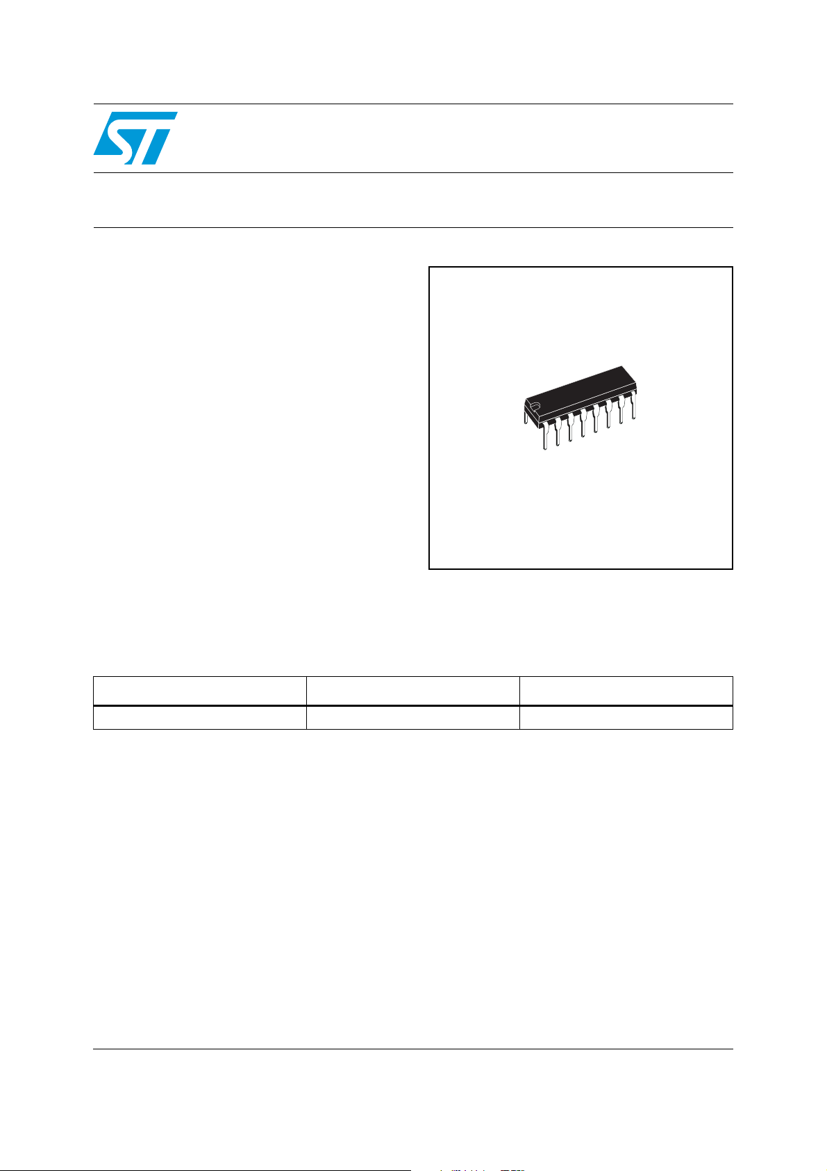
PDIP 16
They are used particular in bipolar stepper motor
applications, where high efficient operation, due
to low forward voltage drop and fast reverse
recovery time, are required.
Table 1. Device summary
Order code Package Packing
E-L6210 PDIP 16 Tube
The L6210 is available in a 16 pin powerdip
package (12 + 2 + 2) designed for the 0 to 70°C
ambient temperature range.
April 2008 Rev 2 1/8
www.st.com
8

Contents L6210
Contents
1 Block and pin connection diagram . . . . . . . . . . . . . . . . . . . . . . . . . . . . . 3
2 Electrical specifications . . . . . . . . . . . . . . . . . . . . . . . . . . . . . . . . . . . . . . 4
2.1 Absolute maximum ratings . . . . . . . . . . . . . . . . . . . . . . . . . . . . . . . . . . . . . 4
2.2 Thermal data . . . . . . . . . . . . . . . . . . . . . . . . . . . . . . . . . . . . . . . . . . . . . . . 4
2.3 Electrical characteristics . . . . . . . . . . . . . . . . . . . . . . . . . . . . . . . . . . . . . . . 4
3 Mounting instructions . . . . . . . . . . . . . . . . . . . . . . . . . . . . . . . . . . . . . . . . 5
4 Package information . . . . . . . . . . . . . . . . . . . . . . . . . . . . . . . . . . . . . . . . . 6
5 Revision history . . . . . . . . . . . . . . . . . . . . . . . . . . . . . . . . . . . . . . . . . . . . 7
2/8
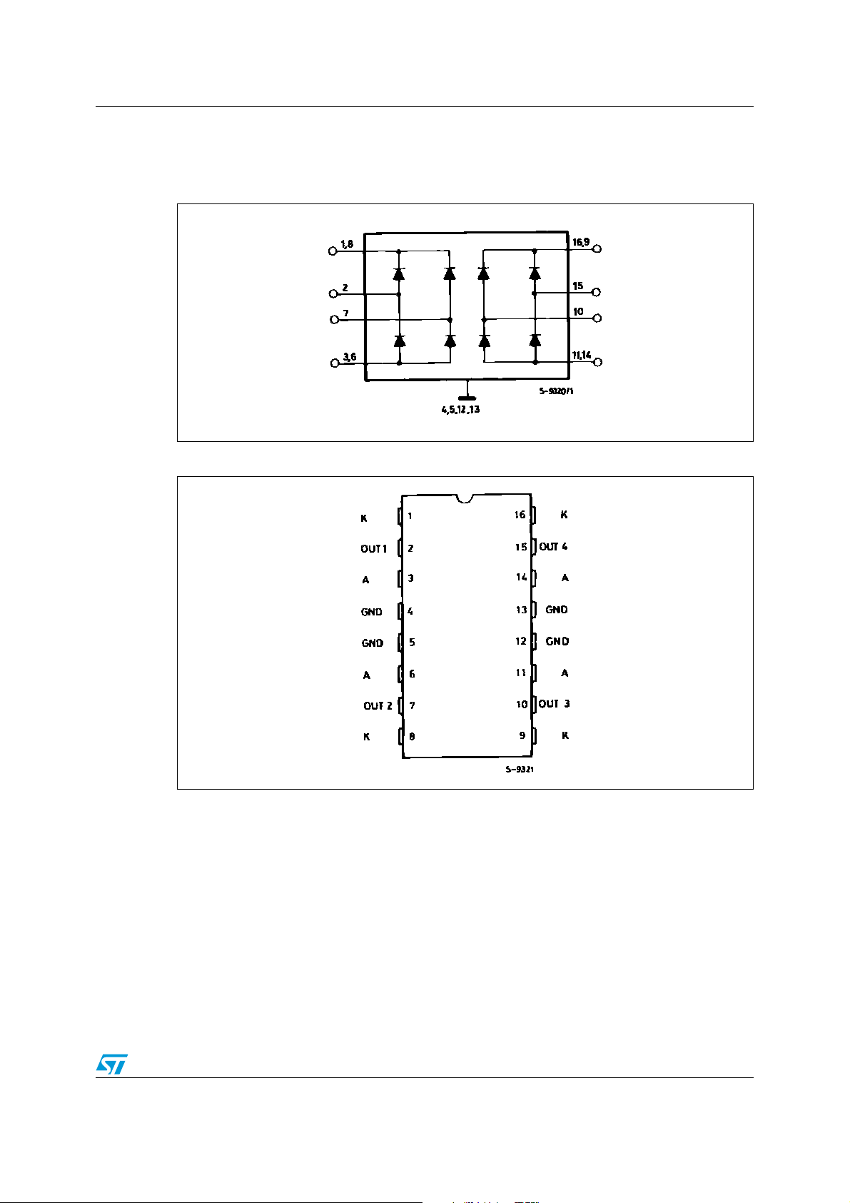
L6210 Block and pin connection diagram
1 Block and pin connection diagram
Figure 1. Block diagram
Figure 2. Pin connection (top view)
3/8

Electrical specifications L6210
2 Electrical specifications
2.1 Absolute maximum ratings
Table 2. Absolute maximum ratings
Symbol Parameter Value Unit
I
Repetitive Forward Current Peak 2 A
F
Peak Reverse Voltage (per diode) 50 V
V
R
Operating Ambient Temperature 70 °C
T
AMB
T
STG
2.2 Thermal data
Table 3. Thermal data
Symbol Parameter Min. Typ. Max. Unit
Storage Temperature Range –55 to +150 °C
R
TH J-CASE
R
TH J-AMB
Thermal Impedance Junction-case 14 °C/W
Thermal Impedance Junction-ambient without
External Heatsink
65 °C/W
2.3 Electrical characteristics
Table 4. Electrical characteristics
(T
= 25°C unless otherwise specified)
J
Symbol Parameter Test conditions Min. Typ. Max. Unit
I
= 100 mA 0.65 0.8 V
F
V
F
Leakage Current VR = 40 V, T
I
L
Forward Voltage Drop
Note: At forward currents of greater than 1 A, a parasitic current of approximately 10 mA may be
collected by adiacent diodes.
= 500 mA 0.8 1 V
I
F
I
= 1 A 1 1.2 V
F
= 25 °C 1 mA
AMB
4/8

L6210 Mounting instructions
3 Mounting instructions
The R
area of the printed circuit boards as shown in Figure 3 or to an external heatsink (Figure 4).
During soldering the pin temperature must not exceed 260°C and the soldering time must
not be longer then 12 s. The external heatsink or printed circuit copper area must be
connected to electrical ground.
Figure 3. Example of PC board copper area which is used as heatsink
b of the L6210 can be reduced by soldering the GND pins to suitable copper
th j-am
Figure 4. Example of an external heatsink
5/8

Package information L6210
4 Package information
In order to meet environmental requirements, ST (also) offers these devices in ECOPACK®
packages. ECOPACK
®
packages are lead-free. The category of second Level Interconnect
is marked on the package and on the inner box label, in compliance with JEDEC Standard
JESD97. The maximum ratings related to soldering conditions are also marked on the inner
box label.
ECOPACK is an ST trademark. ECOPACK specifications are available at: www.st.com.
Figure 5. PDIP 16 mechanical data and package dimensions
DIM.
A 5.330 0.2098
A1 0.380 0.0150
A2 2.920 3.300 4.950 0.1150 0.1299 0.1949
b 0.360 0.460 0.560 0.0142 0.0181 0.0220
b2 1.140 1.520 1.780 0.0449 0.0598 0.0701
c 0.200 0.250 0.360 0.0079 0.0098 0.01 42
(*)
D
E 7.620 7.870 8.260 0.3000 0.3098 0.3252
(*)
E1
e 2.540 0.1000
e1 17.780 0.7000
eA 7.620 0.3000
eB 10.920 0.4299
L 2.920 3.300 3.810 0.1150 0.1299 0.1500
(*)“D” and “E1” dimensions do not include mold flash or protusions.
Mold flash or protusions shall not exceed 0.25mm.
mm inch
MIN. TYP. MAX. MIN. TYP. MAX.
18.670 19.180 19.690 0.7350 0.7 551 0.7752
6.100 6.350 7.110 0.2402 0.2500 0.2799
OUTLINE AND
MECHANICAL DATA
PDIP 16
6/8
0015895_E
0015895 E

L6210 Revision history
5 Revision history
Table 5. Document revision history
Date Revision Changes
31-Jul-2003 1 Initial release.
23-Apr-2008 2 Package information updated.
7/8

L6210
Please Read Carefully:
Information in this document is provided solely in connection with ST products. STMicroelectronics NV and its subsidiaries (“ST”) reserve the
right to make changes, corrections, modifications or improvements, to this document, and the products and services described herein at any
time, without notice.
All ST products are sold pursuant to ST’s terms and conditions of sale.
Purchasers are solely responsible for the choice, selection and use of the ST products and services described herein, and ST assumes no
liability whatsoever relating to the choice, selection or use of the ST products and services described herein.
No license, express or implied, by estoppel or otherwise, to any intellectual property rights is granted under this document. If any part of this
document refers to any third party products or services it shall not be deemed a license grant by ST for the use of such third party products
or services, or any intellectual property contained therein or considered as a warranty covering the use in any manner whatsoever of such
third party products or services or any intellectual property contained therein.
UNLESS OTHERWISE SET FORTH IN ST’S TERMS AND CONDITIONS OF SALE ST DISCLAIMS ANY EXPRESS OR IMPLIED
WARRANTY WITH RESPECT TO THE USE AND/OR SALE OF ST PRODUCTS INCLUDING WITHOUT LIMITATION IMPLIED
WARRANTIES OF MERCHANTABILITY, FITNESS FOR A PARTICULAR PURPOSE (AND THEIR EQUIVALENTS UNDER THE LAWS
OF ANY JURISDICTION), OR INFRINGEMENT OF ANY PATENT, COPYRIGHT OR OTHER INTELLECTUAL PROPERTY RIGHT.
UNLESS EXPRESSLY APPROVED IN WRITING BY AN AUTHORIZED ST REPRESENTATIVE, ST PRODUCTS ARE NOT
RECOMMENDED, AUTHORIZED OR WARRANTED FOR USE IN MILITARY, AIR CRAFT, SPACE, LIFE SAVING, OR LIFE SUSTAINING
APPLICATIONS, NOR IN PRODUCTS OR SYSTEMS WHERE FAILURE OR MALFUNCTION MAY RESULT IN PERSONAL INJURY,
DEATH, OR SEVERE PROPERTY OR ENVIRONMENTAL DAMAGE. ST PRODUCTS WHICH ARE NOT SPECIFIED AS "AUTOMOTIVE
GRADE" MAY ONLY BE USED IN AUTOMOTIVE APPLICATIONS AT USER’S OWN RISK.
Resale of ST products with provisions different from the statements and/or technical features set forth in this document shall immediately void
any warranty granted by ST for the ST product or service described herein and shall not create or extend in any manner whatsoever, any
liability of ST.
ST and the ST logo are trademarks or registered trademarks of ST in various countries.
Information in this document supersedes and replaces all information previously supplied.
The ST logo is a registered trademark of STMicroelectronics. All other names are the property of their respective owners.
© 2008 STMicroelectronics - All rights reserved
STMicroelectronics group of companies
Australia - Belgium - Brazil - Canada - China - Czech Republic - Finland - France - Germany - Hong Kong - India - Israel - Italy - Japan -
Malaysia - Malta - Morocco - Singapore - Spain - Sweden - Switzerland - United Kingdom - United States of America
www.st.com
8/8
 Loading...