

L5991
®
PRIMARY CONTR OLL ER WI TH STANDBY
CURRENT-MODE CONTROL PWM
SWITCHING FREQUENCY UP TO 1MHz
LOW START-UP CURRENT (< 120µA)
HIGH-CURRENT OUTPUT DRIVE SUITABLE
FOR POW E R MO S F ET (1 A )
FULLY LATCHED PWM LOGIC WITH DOU-
BLE PULSE SUPPRESSION
PROGRAMMABLE DUTY CY CLE
100% AND 50% MAX IMUM DU TY C YCLE LI MIT
STANDBY FUNCTION
PROGRAMMABLE SOFT START
PRIMARY OVERCURRENT FAULT DETEC-
TION WITH RE-START DELAY
PWM UV LO W I T H H YS T ERESIS
IN/OUT SYNCHRONIZATION
LATCHED DISABLE
INTERNAL 100ns LEADING EDGE BLANK-
ING OF CURRENT SENSE
PACKAGE: DIP16 AND SO16
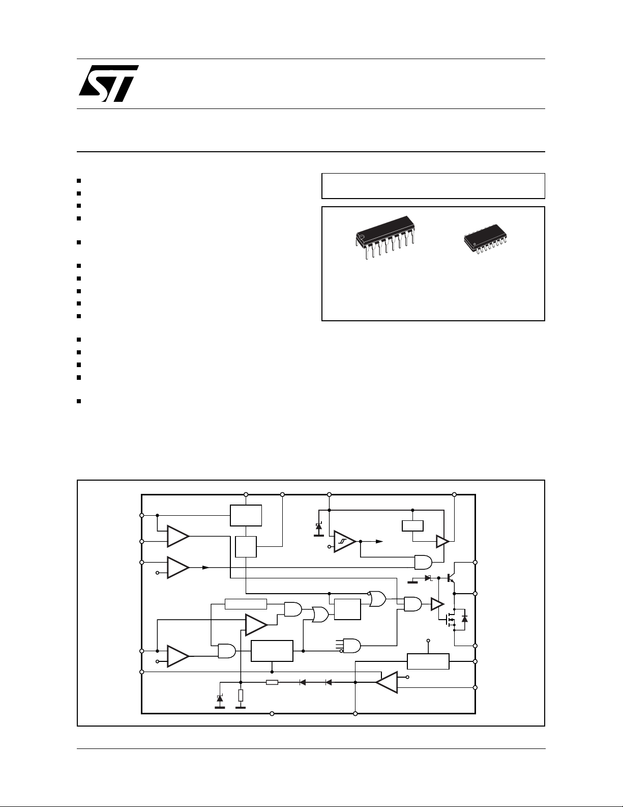
DESCRIPTION
This primary controller I.C., developed in BCD60II
technology, has been designed to implement off
L5991A
MULTIPOWER BCD TECHNOLOGY
DIP16 SO16
ORDERING NUMBERS:
L5991D/L5991AD (SO16)
line or DC-DC power supply applications using a
fixed frequency current mode control.
Based on a standard current mode PWM controller this device includes some features such as
programmable soft start, IN/OUT synchronization,
disable (to be used for over voltage protection and
for power management), precise maximum Duty
Cycle Control, 100ns leading edge blanking on
current sense, pulse by pulse current limit, overcurrent protection with soft start intervention, and
Standby function for oscillator frequency reduction
when the converter is lightly loaded.
L5991/L5991A (DIP16)
BLOCK DIAGRAM
2
RCT
3
DC
14
DIS
2.5V
13
ISEN
1.2V
SS
7
August 2001
+
-
-
+
OVER CURRENT
+
-
DIS
BLANKING
1V R
SYNC DC-LIM
TIMING
T
PWM
FAULT
SOFT-START
2R
12
SGND COMP
25V
15V/10V
VREF OK
CLK
DIS
V
CC
Vref
+
PWM UVLO
-
SQ
R
STAND-BY
+
2.5V
E/A
-
6
13V
VREF
VREF
48151
D97IN725A
9
V
C
10
OUT
11
PGND
16
ST-BY
5
VFB
1/23
L5991 - L5991A
ABSOLUTE MAXIMUM RATINGS
Symbol Parameter Value Unit
V
CC
I
OUT
P
tot
T
j
T
stg
(*) maximum package power dissipation limits must be observed
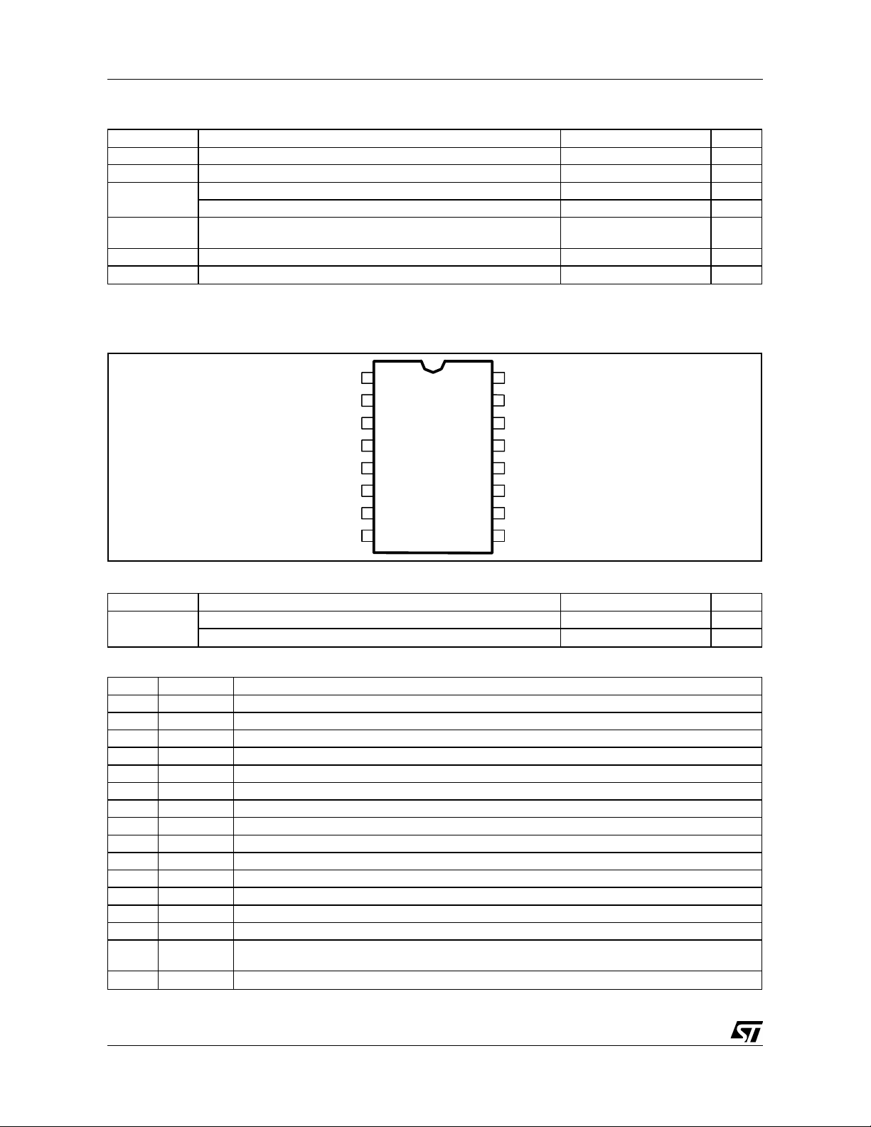
PIN CONNECTION
Supply Voltage (ICC < 50mA) (*) selflimit V
Output Peak Pulse Current 1.5 A
Analog Inputs & Outputs (6,7) -0.3 to 8 V
Analog Inputs & Outputs (1,2,3,4,5,15,14, 13, 16) -0.3 to 6 V
Power Dissipation @ T
@ T
= 70°C (DIP16)
amb
= 50°C (SO16)
amb
1
0.83
Junction Temperature, Operating Range -40 to 150 °C
Storage Temperature, Operating Range -55 to 150 °C
W
W
SYNC
RCT
DC
VREF
VFB
COMP
SS
V
CC
1
2
3
4
5
6
7OUT
8V
15
14
13
12
11
10
ST-BY16
DC-LIM
DIS
ISEN
SGND
PGND
9
C
THERMAL DATA
Symbol Parameter Value Unit
R
th j-amb
Thermal Resistance Junction -Ambient
Thermal Resistance Junction -Ambient
(DIP16)
(SO16)
80 °C/W
120 °C/W
PIN FU NCTIONS
N. Name Function
1 SYNC Synchronization. A synchronization pulse terminates the PWM cycle and discharges Ct
2 RCT Oscillator pin for external C
3 DC Duty Cycle control
4 VREF 5.0V +/-1.5% reference voltage @ 25°C
5 VFB Error Amplifier Inverting input
6 COMP Error Amplifier Output
7 SS Soft start pin for external capacitor Css
8V
9V
CC
C
Supply for internal "Signal" circuitry
Supply for Power section
10 OUT High current totem pole output
11 PGND Power ground
12 SGND Signal ground
13 ISEN Current sense
14 DIS Disable. It must never be left floating. TIE to SGND if not used.
15 DC-LIM Connecting this pin to Vref, DC is limited to 50%. If it is left floating or grounded no limitation is
imposed
16 ST-BY Standby. Connect a resistor to RCT. Connect to VREF or floating if not used.
, RA, RB components
T
2/23
L5991 - L5991A
ELECTRICAL CHARACTERI STICS
CC
= 15V; Tj = 0 to 105°C; RT = 13.3kΩ (*) CT = 1nF;
(V
unless otherwise specified.)
Symbol Parameter Test Condition Min. Typ. Max. Unit
REFERENCE SECTION
V
REF
T
S
I
OS
OSCILLATOR SECTION
ERROR AMPLIFIER SECTION
V
I
G
OPL
SVR Supply Voltage Rejection V
V
OL
V
OH
I
O
S
R
PWM CURRENT SENSE SECTION
I
b
I
S
V
t
SOFT START SECTION
I
SSC
I
SSD
V
SSSAT
V
SSCLAMP
LEADING EDGE BLANKING
OUTPUT SECTION
V
OL
V
OH
V
OUT CLAMP
(*) RT = RA//RB, RA = RB = 27kΩ, see Fig. 23.
Output Voltage Tj = 25°C; IO = 1mA 4.925 5.0 5.075 V
Line Regulation V
Load Regulation I
= 12 to 20V; Tj = 25°C 2.0 10 mV
CC
= 1 to 10mA; Tj = 25°C 2.0 10 mV
O
Temperature Stability 0.4 mV/°C
Total Variation Line, Load, Temperature 4.80 5.0 5.130 V
Short Circuit Current Vref = 0V 30 150 mA
Power Down/UVLO V
= 6V; I
CC
Initial Accuracy pin 15 = Vref; T
pin 15 = Vref; V
V
pin 15 = Vref; V
V
Duty Cycle pin 3 = 0,7V, pin 15 = V
pin 3 = 0.7V, pin 15 = OPEN
pin 3 = 3.2V, pin 15 = V
pin 3 = 3.2V, pin 15 = OPEN
= 0.5mA 0.2 0.5 V
sink
= 25°C; V
j
= 12 to 20V
CC
comp
= 12 to 20V
CC
comp
= 4.5V 95 100 105 kHz
comp
93 100 107 kHz
= 4.5V
46.5 50 53.5 kHz
= 2V
REF
0
0
REF
47
93
Duty Cycle Accuracy pin 3 = 2.79V, pin 15 = OPEN 75 80 85 %
Oscillator Ramp Peak 2.8 3.0 3.2 V
Oscillator Ramp Valley 0.75 0.9 1.05 V
Input Bias Current V
Input Voltage V
Open Loop Gain V
Output Low Voltage I
Output High Voltage I
Output Source Current V
Output Sink Current V
to GND 0.2 3.0 µA
FB
= V
COMP
COMP
CC
sink
source
COMP
COMP
FB
= 2 to 4V 60 90 dB
= 12 to 20V 85 dB
= 2mA 1.1 V
= 0.5mA, VFB = 2.3V 5 6 V
> 4V, VFB = 2.3V 0.5 1.3 2.5 mA
= 1.1V, VFB = 2.7V 2 6 mA
2.42 2.5 2.58 V
Unit Gain Bandwidth 1.7 4 MHz
Slew Rate 8 V/µs
Input Bias Current I
Maximum Input Signal V
= 0 3 15 µA
sen
= 5V 0.92 1.0 1.08 V
COMP
Delay to Output 70 100 ns
Gain 2.85 3 3.15 V/V
Fault Threshold Voltage 1.1 1.2 1.3 V
SS Charge Current Tj = 25°C 142026µA
SS Discharge Current VSS = 0.6V Tj = 25°C 5 10 15 µA
SS Saturation Voltage DC = 0% 0.6 V
SS Clamp Voltage 7 V
Internal Masking Time 100 ns
Output Low Voltage IO = 250mA 1.0 V
Output High Voltage IO = 20mA; VCC = 12V 10 10.5 V
I
= 200mA; VCC = 12V 9 10 V
O
Output Clamp Voltage IO = 5mA; VCC = 20V 13 V
Collector Leakage V
= 20V VC = 24V 2 20 µA
CC
%
%
%
%
3/23
L5991 - L5991A
ELECTRICAL CHARACTERI STICS
(continued.)
Symbol Parameter Test Condition Min. Typ. Max. Unit
OUTPUT SECTION
Fall Time C
O
C
O
= 1nF
= 2.5nF
Rise Time CO = 1nF
C
= 2.5nF
O
UVLO Saturation VCC = VC = 0 to V
CCON; Isink
= 10mA 1.0 V
20
35
50
70
60 ns
100 ns
SUPPLY SECTION
V
CCON
V
CCOFF
V
Startup voltage
Minimum Operating
Voltage
hys
I
S
I
op
I
q
V
Z
UVLO Hysteresis
Start Up Current Before Turn-on at:
V
= VC = V
CC
CCON
-0.5V
Operating Current CT = 1nF, RT = 13.3kΩ, CO =1nF 9 13 mA
Quiescent Current (After turn on), CT = 1nF,
R
= 13.3kΩ, CO =0nF
T
Zener Voltage I8 = 20mA 21 25 30 V
L5991
L5991A
L5991
L5991A
L5991
L5991A
14
7.8
9
7
4.5
0.5
15
8.4
10
7.6
5
0.8
16
9
11
8.2
40 75 120 µA
7.0 10 mA
STANDBY FUNCTION
I
V
REF-VST-BY
V
T1
Standby Threshold V
= 2mA 45 mV
ST-BY
Falling 2.5 V
comp
V
Rising 4.0 V
comp
SYNCHRONIZATION SECTION
Master Operation
V
1
I
1
Clock Amplitude I
Clock Source Current Vclock = 3.5V 3 7 mA
= 0.8mA 4 V
SOURCE
Slave Operation
V
1
Sync Pulse Low Level 1 V
High Level 3.5 V
I
1
Sync Pulse Current VSYNC = 3.5V 0.5 mA
OVER CURRENT PROTECTION
V
t
Fault Threshold Voltage 1.1 1.2 1.3 V
DISABLE SECTION
Shutdown threshold 2.4 2.5 2.6 V
= 0 to 3V -1 1 µA
pin14
VCC = 15V 330 µA
I
qSH
Input Bias Current V
Quiescent current After
Disable
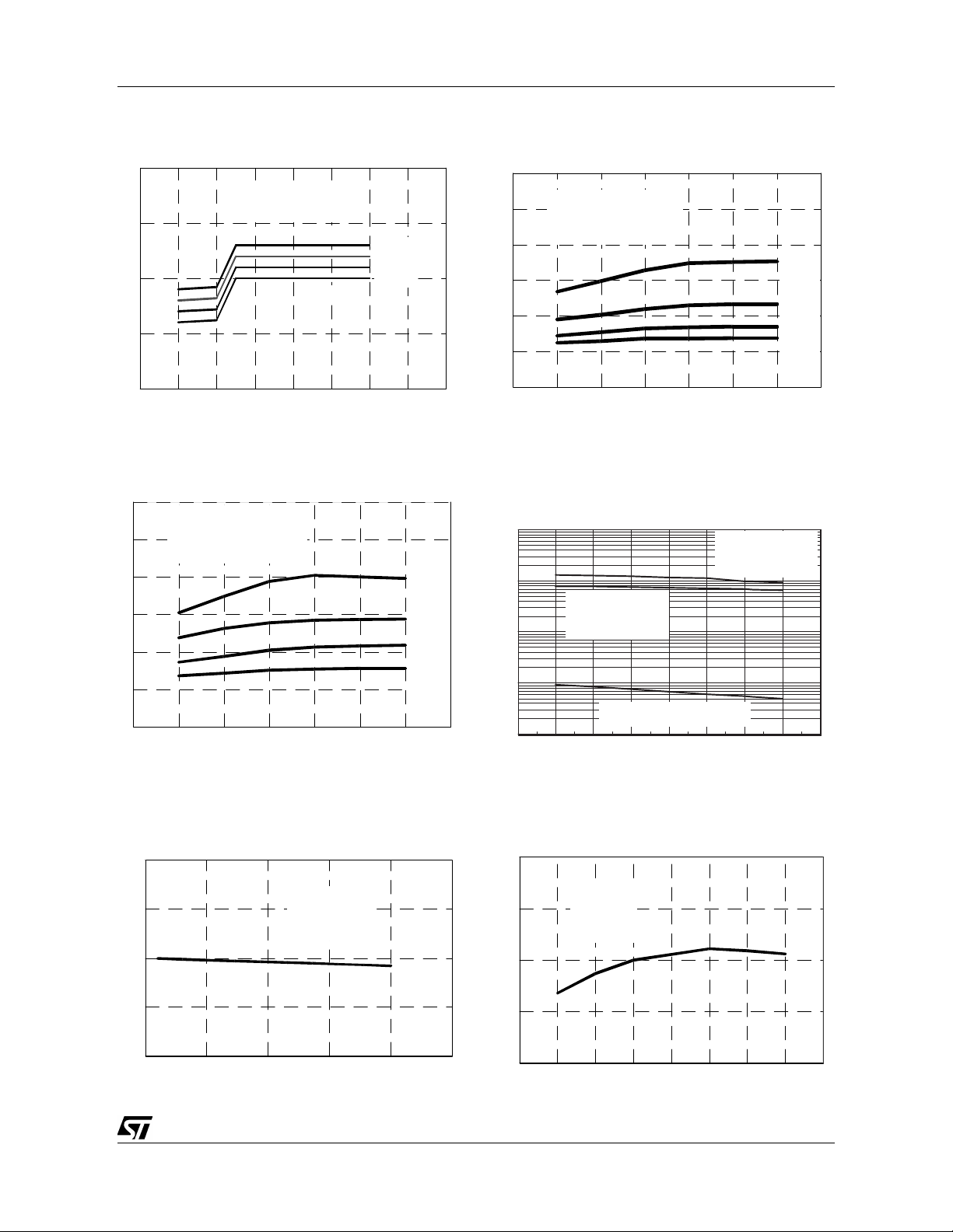
Figure 1. L5991 - Quiescent current vs. input
voltage.
(X = 7.6V and Y= 8.4V for L5991A)
Iq [m A ]
30
20
8
6
4
0.2
0.15
0.1
0.05
0
04 8
V14 = 0, Pin2 = open
Tj = 25°C
X
12 16 20 24
Y
Vcc [V]
28
Figure 2. L5991 - Quiescent current vs. input
voltage (after disable).
(X = 7.6V and Y= 8.4V for L5991A)
Iq [µ A ]
350
300
250
200
150
100
50
0
0 4 8 12 16 20 24
X
Vcc [V]
V14 = Vref
Tj = 25 °C
Y
ns
ns
V
V
V
V
V
V
4/23
)
L5991 - L5991A
Figure 3. Quiescent current vs. input voltage.
Iq [m A ]
9.0
V14 = 0, V5 = Vref
8.5
8.0
7.5
7.0
8 1012141618202224
Rt = 4.5Kohm,Tj = 25°C
1Mhz
500K hz
300K hz
100K hz
Vc c [V]
Figure 5. Quiescent current vs. input voltage
and switching fre que nc y .
Iq [mA ]
36
Co = 1nF, Tj = 25°C
30
24
18
12
6
0
8 10121416182022
DC = 100 %
1MHz
500KHz
300KHz
100KHz
Vcc [V]
Figure 4. Quiescent current vs. input voltage
and switching frequency.
Iq [m A]
36
30
24
18
12
6
0
Co = 1nF, Tj = 25°C
DC = 0%
1MHz
500KHz
300KHz
100KHz
8 10121416182022
Vcc [V]
Figure 6. IC Consumption vs. Temperature.
[mA]
100
10
Quiescent current
Vcc =15V, after turn-on
RT=13.3 kΩ, CT=1nF
1
DC = 0
0.1
Start-up current
Vc=Vcc= Vccon-0.5V , before turn-on
0.01
-50 -25 0 25 50 75 100 125 150
Junction temperature [˚C]
Operating current
Vcc =15V, after turn-on
RT=13.3kΩ, CT=1nF
DC=75%, Co=1nF
Figure 7. Reference voltage vs. load current.
Vref [V]
5.1
5.05
5
4.95
4.9
0 5 10 15 20 25
Vcc=15V
Tj = 25°C
Iref [mA]
Figure 8. Vref vs. junction temperature.
Vref [V])
5.1
5.05
5
4.95
4.9
-50 -25 0 25 50 75 100 125 150
Vcc = 15V
Iref = 1mA
Tj (°C
5/23
L5991 - L5991A
Figure 9. Vref vs. junction temperature.
Vref [V]
5.1
Vcc = 15V
5.05
5
4.95
4.9
-50 -25 0 25 50 75 100 125 150
Iref= 20mA
Tj (°C)
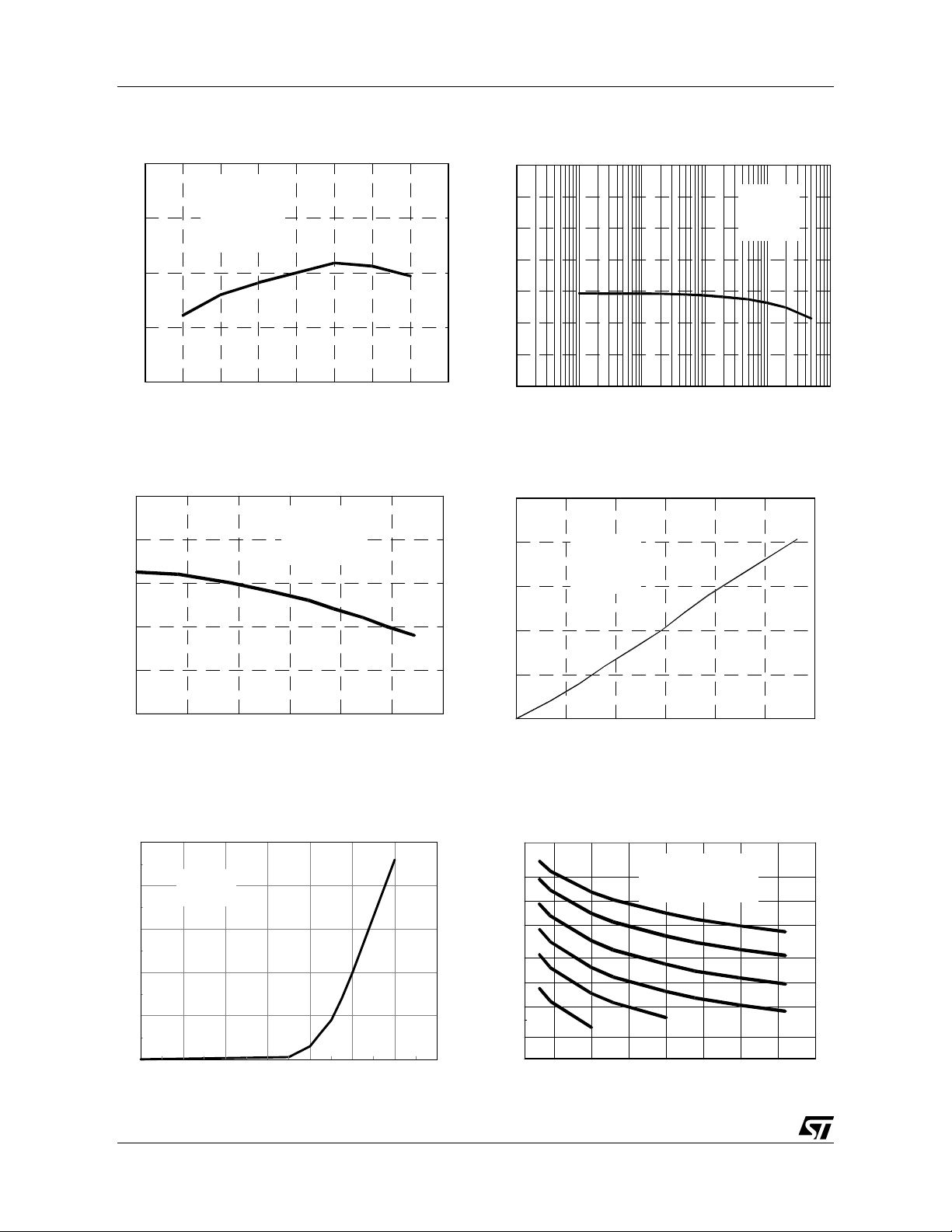
Figure 11. Output saturation.
Vsa t = V [V]
16
14
12
10
Vcc = Vc = 15V
Tj = 25°C
Figure 10. Vref SVRR vs. switching frequency.
SVRR (dB)
120
80
40
0
1 10 100 1000 10000
fsw (Hz)
Vcc=15V
Vp-p=1V
Figure 12. Output saturation.
Vs at = V [V]
2.5
2
1.5
10
Vcc = Vc = 15V
Tj = 25°C
10
8
6
0 0.2 0.4 0.6 0.8 1 1.2
Isource [A]
Figure 13. UVLO Saturation
Ipin10 [mA]
50
40
30
20
10
0
Vcc < Vccon
before turn-on
0 200 400 600 800 1,000 1,200 1,400
Vp in 1 0 [mV]
1
0.5
0
0 0.2 0.4 0.6 0.8 1 1.2
Isink [A]
Figure 14. Timing resistor vs. switching frequency.
fsw (KHz)
5000
2000
1000
500
200
100
50
20
10
5.6nF
10 20 30 40
Vcc = 15V, V15 =0V
Tj = 25°C
2.2nF
Rt (kohm)
100pF
220pF
470pF
1nF
6/23
)
L5991 - L5991A
Figure 15. Switching frequency vs. tempera-
ture.
fsw (KHz)
320
Rt= 4.5Kohm, Ct = 1nF
310
300
290
280
-50 -25 0 25 50 75 100 125 150
Vcc = 15V, V15=Vref
Tj (°C)
Figure 17. Dead time vs Ct.
Dea d time [ns]
1,500
1,200
900
600
300
Rt =4.5Kohm
V15 = 0V
V15 = Vref
Figure 16. Switching freque nc y v s. t emp er atu re .
fsw (KHz)
320
Rt= 4.5Kohm, Ct = 1nF
310
Vcc = 15V, V15= 0
300
290
280
-50 -25 0 25 50 75 100 125 150
Tj (°C)
Figure 18. Maximum Duty Cycle vs Vpin3.
DC Control Voltage Vpin3 [V]
3.5
V15 = 0V
2.5
1.5
V15 = Vref
3
2
Rt = 4.5Kohm,
Ct = 1nF
246810
Timing capacitor Ct [nF]
Figure 19. Delay to out put vs jun ction temperat ure.
Delay to output (ns)
42
40
38
36
34
32
30
28
-50 -25 0 25 50 75 100 125 150
Tj (°C
PIN10 = OPEN
1V pulse
on PIN13
1
0 102030405060708090100
Duty Cycle [%]
Figure 20. E/A frequency response.
G [dB]
150
100
50
0
0.01 0.1 1 10 10 0 1000 10000 100000
f (KHz)
Phase
140
120
100
80
60
40
20
7/23

L5991 - L5991A
STANDBY FUNCTION
The standby function, optimized for flyback topology, automatically detects a light load condition
for the converter and decreases the oscillator frequency on that occurrence. The normal oscillation
frequency is automatically resumed when the output load builds up a nd exceeds a defined threshold.
This function allows to minimize power losses related to switching frequency, which represent the
majority of losses in a lightly loaded flyback, without giving up the advantages of a higher switching
frequency at heavy load.
This is accomplished by monitoring the output of
the Error Amplifier (V
) that depends linearly
COMP
on the peak primary current, except for an offset.
If the the peak primary current decreases (as a re-
sult of a decrease of the power demanded by the
load) and V
(V
), the oscillator frequency will be set to a
T1
lower value (f
increases and V
falls below a fixed threshold
COMP
). When the peak primary current
SB
exceeds a second threshold
COMP
(VT2) the oscillator frequency is set to the normal
value (f
). An appropriate hysteresis (VT2-VT1)
osc
prevents undesired frequency change when
power is such that V
moves close to the
COMP
threshold. This operation is shown in fig. 21.
Both the normal and the standby frequency are
externally programmable. V
and VT2 are inter-
T1
nally fixed but it is possible to adjust the thresholds in terms of input power level.
Figure 21. Standby dynamic operation.
Pin
f
osc
Normal operation
P
NO
P
SB
V
T
1234
1
Stand-by
f
SB
V
T
2
VCOMP
matically the master.
During the ramp-up of the oscillator the pin is
pulled low by a 600µA internal sink current generator. During the falling edge, that is when the
pulse is released, the 600µA pull-down is disconnected. The pin becomes a generator whose
source capability is typically 7mA (with a voltage
still higher than 3.5V).
In fig. 22, some practical examples of synchronizing the L5991 are given.
Since the device automatically diminishes its operating frequency under light load conditions, it is
reasonable to suppose that synchronization will
refer to normal operation and not to standby.
APPLICATION INFORMATION
Detailed Pin Function Description
Pin 1.
SYNC (In/Out Synchronization). This function allows the IC’s oscillator either to synchronize
other controllers (master) or to be synchronized to
an external frequency (slave).
As a master, the pin delivers positive pulses during the falling edge of the oscillator (see pin 2). In
slave operation the circuit is edge triggered. Refer
to fig. 23 to see how it works. When several IC
work in parallel no master-slave designation is
needed because the fastest one becomes auto-
Figure 22. Synchronizing the L5991.
R
B
ST-BY
1
16
L5991 L5991
VREF
4
2
R
A
C
T
(a) (b) (c)
SYNCSYNC
1
2
RCTRCT
R
OSC
L4981A
(MASTER)
16
1817
C
OSC
(SLAVE)
1
RCT
ST-BY
L5991
Pin 2.
RCT (Oscillator). Two resistors (R
and one capacitor (C
), connected as shown in
T
fig. 23, allow to set separately the operating frequency of the oscillator in normal operation (f
and in standby mode (f
C
is charged from Vref through RA and RB in nor-
T
SB
).
mal operation (STANDBY = HIGH), through R
only in standby ( STANDBY = LOW). See pin 16
description to see how the STANDBY signal is generated.
When the voltage on C
reaches 3V, the capaci-
T
tor is quickly internally discharged. As the voltage
has dropped to 1V it starts being charged again.
R
A
16
4
2
R
B
VREFSYNC
R
A
C
T
RCT
R
B
C
T
D97IN728A
4
L5991
(MASTER)
16
ST-BY
VREF
12
SYNC
SYNC
16
R
OSC
L4981A
(SLAVE)
and RB)
A
17 18
C
osc
OSC
)
A
8/23

Figure 23. Oscillator and synchronization internal schematic.
4
V
REF
L5991 - L5991A
SYNC
1
R1
CLAMP
R
A
RCT
2
R
B
C
T
16ST-BY
D1
50Ω
STANDBY
R2R3
The oscillation frequency can be established with
the aid of the diagrams of fig. 14, where RT will be
intended as the parallel of R
and RB in normal
A
operation and RT = RA in standby, or considering
the following approximate relationships:
f
osc
≅
C
⋅ (0.693 ⋅ (RA // R
T
1
B
) +
K
(1),
T
which gives the normal operating frequency, and:
f
≅
SB
C
⋅ (0.693 ⋅ RA + K
T
1
T
(2
)
)
,
which gives the standby frequency, that is the one
the converter will operate at when lightly loaded.
In the above expressions, RA // RB means:
R
⋅
R
B
A
=
RB
R
//
while K
A
is defined as:
T
90 V15
=
K
T
160
V15 =
=
VREF
GND
R
+
A
,
R
B
/OPEN
(3),
D
Q
R
600µA
+
-
D97IN729A
CLK
from fig. 14 or resulting from (1) and (2).
To prevent the oscillator frequency from switching
back and forth from f
to fSB, the ratio f
osc
must not exceed 5.5.
If during normal operation the IC is to be synchro-
nized to an external oscillator, R
should be selected for a f
lower than the master
osc
, RB and C
A
frequency in any condition (typically, 10-20% ),
depending also on the tolerance of the parts.
Pin 3.
DC (Duty Cycle Control). By biasing this
pin with a voltage between 1 and 3 V it is possible
to set the maximum duty cycle between 0 and the
upper extreme D
If D
is the desired maximum duty cycle, the
max
(see pin 15).
x
voltage V3 to be applied to pin 3 is:
V
= 5 - 2
3
is determined by internal comparison be-
D
max
(2-Dmax)
(5)
tween V3 and the oscillator ramp (see fig. 24),
thus in case the device is synchronized to an external frequency f
(and therefore the oscillator
ext
amplitude is reduced), (5) changes into:
osc
/ f
SB
T
and is related to the duration of the falling- edge of
the sawtooth:
−
9
⋅
≈
30
Td
T
is also the duration of the sync pulses deliv-
d
10
+ KT
⋅
C
(4).
T
ered at pin 1 and defines the upper extreme of the
duty cycle range, D
(see pin 15 for DX definition
x
and calculation) since the output is held low during the falling edge.
In case V15 is connected to VREF, however, the
switching frequency will be a half the values taken
V
3
=
5
− 4 ⋅ exp
−
R
D
⋅ CT
T
max
(6)
⋅
f
ext
A voltage below 1V will inhibit the driver output
stage. This could be used for a not-latched device
disable, for example in case of overvoltage protection (see application ideas).
If no limitation on the maximum duty cycle is required (i.e. D
= DX), the pin has to be left float-
MAX
ing. An internal pull-up (see fig. 24 ) holds the voltage above 3V. Should the pin pick up noise (e.g.
9/23

L5991 - L5991A
during ESD tests), it can be connected to VREF
through a 4.7kΩ resistor.
Figure 24. Duty cycle control.
4
V
REF
R1
DC
R
R2
A
ST-BY
R
B
RCT
C
T
Pin 4.
VREF (Reference Voltage). The device is
3µA
3
16
+
2
-
D97IN727A
23K
28K
TO PWM LOGIC
provided with an accurate voltage reference
(5V±1.5%) able to deliver some mA to an external
circuit.
A small film capacitor (0.1 µF typ.), connected
between this pin and SGND, is recommended to
ensure the stability of the generator and to prevent
noise from affecting the reference.
Before device turn-on, this pin has a sink current capability o f 0.5mA .
Pin 5.
VFB (Error Amplifier Inverting Input). The
feedback signal is applied to this pin and is compared to the E/A internal reference (2.5V). The
E/A output generates the control voltage which
fixes the duty cycle.
The E/A features high gain-bandwidth product,
which allows to broaden the bandwidth of the
overall control loop, high slew-rate and current capability, which improves its large s ignal behavior.
Usually the compensation network, which stabilizes the overall control loop, is connected between this pin and COMP (pin 6).
Pin 6.
COMP (Error Amplifier Output). Usually,
this pin is used for frequency compensation and
the relevant network is connected between this
pin and VFB (pin 5). Compensation networks towards ground are not possible since the L5991
E/A is a voltage mode amplifier (low output impedance). See application ideas for some example of compensation techniques.
It is worth mentioning that the calculation of the
part values of the compensation network must
take the standby frequency operation into account. In particular, this means that the open-loop
crossover frequency must not exceed f
/5.
f
SB
SB
/4
The voltage on pin 6 is monitored in order to re-
10/23
duce the oscillator frequency when the converter
is lightly loaded (standby).
Pin 7.
SS (Soft-Start). At device start-up, a capacitor (Css) connected between this pin and
SGND (pin 12) is charged by an internal current
generator, ISSC, up to about 7V. During this
ramp, the E/A output is clamped by the voltage
across Css itself and allowed to rise linearly, starting from zero, up to the steady-state value imposed by the control loop. The maximum time interval during which the E/A is clamped, referred to
as soft-start time, is approximately:
3 ⋅ R
≅
T
ss
where R
13) and I
through R
is the current sense resistor (see pin
sense
is the switch peak current (flowing
Qpk
sense
load. Usually, C
), which depends on the output
⋅ I
sense
SS
Qpk
I
SSC
⋅ Css (7)
is selected for a TSS in the or-
der of milliseconds.
As mentioned before, the soft-start intervenes
also in case of severe overload or short circuit on
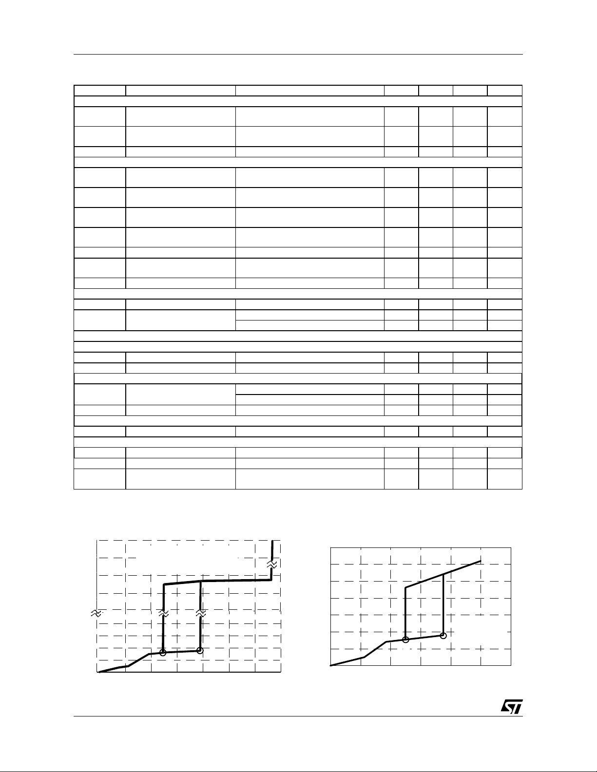
the output. Referring to fig. 25, pulse-by-pulse
current limitation is somehow effective as long as
Figure 25. Regulation characteristic and re-
lated quantiti e s .
V
OUT
D.C.M. C.C.M.
T
ON
D97IN495
A
D
I
SHORTIOUT(max)
B
the ON-time of the power switch can be reduced
(from A to B). After the minimum ON-time is
reached (from B onwards) the current is out of
control.
To prevent this risk, a comparator trips an overcurrent handling procedure, named ’hiccup’ mode
operation, when a voltage above 1.2V (point C) is
detected on current sense input (ISEN, pin 13).
Basically, the IC is turned off and then soft-started
as long as the fault condition is detected. As a result, the operating point is moved abruptly to D,
creating a foldback effect. Fig. 26 illustrates the
operation.
The oscillation frequency appearing on the softstart capacitor in case of permanent fault, referred
to as ’hiccup" period, is approximately given by:
÷
hic
I
SSC
1
⋅
≅ 4.5
T
1
+
⋅ C
ss
I
SSD
C
(8
I
)
I
Qpk
1-2 ·I
I
Qpk(max)
T
ON(min)
OUT
Qpk

L5991 - L5991A
Since the system tries restarting each hiccup cycle, there is not any latchoff risk.
"Hiccup" keeps the system in control in case of
short circuits but does not eliminate power components overstress during pulse-by-pulse limitation (from A to C). Other external protection circuits are needed if a better control of overloads is
required.
Pin 8.
VCC (Controller Supply). This pin supplies
the signal part of the IC. The device is enabled a s
VCC voltage exceeds the start threshold and
works as long as the vol tage is above the UVLO
threshold. Otherwise the device is shut down and
the current consumption is extremely low
(<150µA). This is particularly useful for reducing
the consumption of the start-up circuit (in the simplest case, just one res istor), which is one of the
most significant contributions to power losses in
standby.
An internal Zener limits the voltage on VCC to
25V. The IC current consumption increases considerably if this limit is exceeded.
A small film capacitor between this pin and SGND
(pin 12), placed as close as possible to the IC, i s
recommended to filter high frequency noise.
Pin 9.
VC (Supply of the Power Stage). It supplies
the driver of the external switch and therefore absorbs a pulsed current. Thus it is recommended to
place a buffer capacitor (towards PGND, pin 11,
as close as possible to the IC) able to sustain
these current pulses and in order to avoid them
inducing disturbances.
This pin can be connected to the buffer capa citor
directly or through a resistor, as shown in fig. 27,
to control separately the turn-on and turn-off
speed of the external switch, typically a Power-
MOS. At turn-on the gate resistance is R
turn-off is R
only.
g
+ Rg’, at
g
Figure 27. Turn-on and turn-off speeds adjust-
ment.
Rg'
DRIVE &
CONTROL
L5991
D97IN726
Pin 10.
V
CC
8
13V
PGND
V
C
9
10
OUT
Rg
11
OUT (Driver Output). This pin is the out-
Rg(ON)=Rg+Rg'
Rg(OFF)=Rg
put of the driver stage of the external power
switch. Usually, this will be a PowerMOS, although the driver is powerful enough to drive
BJT’s (1. 6A source, 2A sink, pea k).
The driver is made up of a totem pole with a highside NPN Darlington and a low-side VDMOS, thus
there is no need of an external diode clamp to
prevent voltage from going below ground. An internal clamp limits the voltage delivered to the
gate at 13V. Thus it is possible to supply the
driver (Pin 9) with higher voltages without any risk
of damage for the gate oxide of the external MOS.
The clamp does not cause any additional increase of power dissipation inside the chip since
the current peak of the gate charge occurs when
the gate voltage is few volts and the clamp is not
active. Besides, no current flows when the gate
voltage is 13V, steady state.
Under UVLO conditions an internal circuit (shown
Figure 26. Hiccup mode operation.
I
OUT
I
SEN
FAULT
SS
5V
0.5V
SHORT
7V
T
hic
D98IN986
time
11/23

L5991 - L5991A
in fig.28) holds the pin low in order to ensure that
the external MOS cannot be turned on accidentally. The peculiarity of this circuit is its ability to
mantain the same sink capability (typically, 20mA
@ 1V) from V
= 0V up to the start-up threshold.
CC
When the threshold is exceeded and the L5991
starts operating, V
is pulled high (refer to fig.
REFOK
28) and the circuit is disabled.
It is then possible to omit the "bleeder" resistor
(connected between the gate and the source of
the MOS) ordinarily used to prevent undesired
switching-on of the external MOS because of
some leakage current.
Figure 28. Pull-Down of the output in UVLO.
OUT
10
V
REFOK
12
SGND
D97IN538
Pin 11.
PGND (Power Ground). The current loop
during the discharge of the gate of the external
MOS is closed through this pin. This loop should
be as short as possible to reduce EMI and run
separately from signal currents return.
Pin 12
. SGND (Signal G round). This ground references the control circuitry of the IC, so all the
ground connections of the external parts related
to control functions must lead to this pin. In laying
out the PCB, care must be taken in preventing
switched high currents from flowing through the
SGND path.
Pin 13.
ISEN (Current Sense). This pin is to be
connected to the "hot" lead of the current sense
resistor R
(being the other one grounded), to
sense
get a voltage ramp which is an image of the current of the switch (I
). When this voltage is equal
Q
to:
V
13pk
= I
Qpk
V
⋅
R
sense
COMP
=
1.4
−
3
(9
)
the conduction of the switch is terminated.
To increase the noise immunity, a "Leading Edge
Blanking" of about 100ns is internally realized as
shown in fig. 29. Because of that, the smoothing
RC filter between this pin and R
could be re-
sense
moved or, at least, considerably reduced.
Pin 14.
DIS (Device Disable). When the voltage
on pin 14 rises above 2.5V the IC is shut down
and it is necessary to pull VCC ( IC supply voltage,
pin 8) below the UVLO threshold to allow the device to restart.
The pin can be driven by an external logic signal
in case of power management, as shown in fig.
30. It is also possible to realize an overvoltage
protection, as shown in the section " Application
Ideas".If used, bypass this pin to gr ound with a filter capacitor to avoid spurious activation due to
noise spikes. If not, it must be connected to
SGND.
Pin 15.
DC-LIM (Maximum Duty Cycle Limit). The
upper extreme, Dx, of the duty cycle range depends on the voltage applied to this pin. Approximately,
D
x
≅
RT + 230
T
)
(
10
R
if DC-LIM is grounded or left floating. Instead,
Figure 29. Interna l LEB.
13
ISEN
12/23
I
1.2V
2V
3V
0
CLK
FROM E/A
+
OVERCURRENT
COMPARATOR
+
-
COMPARATOR
+
-
PWM
TO PWM
LOGIC
TO FAULT
LOGIC
D97IN503

L5991 - L5991A
Figure 30. Disable (Latched).
DISABLE
SIGNAL
DIS
14
+
-
C
2.5V
D
R
UVLO
Q
DISABLE
D97IN502
connecting DC-LIM to VREF (half duty cycle option), Dx will be set approximately at:
R
2
T
+
⋅
260
R
T
D
≅
x
(11
)
Figure 31. Half duty cycle option.
t
V15=GND
V5=V13=GND
d
and the output switching frequency will be halved
with respect to the oscillator one because an internal T flip-flop (see block diagram) is activated.
Fig. 31 shows the operation.
The half duty cycle option speeds up the discharge of the timing capacitor C
(in order to get
T
duty cycles as close to 50% as possible) so the
oscillator frequency - with the same timing components will be slightly higher.
Pin 16
. S-BY (Standby Function). The resistor R
along with R
oscillator in normal operation (f
as the
, sets the operating frequency of the
A
). In fact, as long
osc
STANDBY signal is high, the pin is internally connected to the reference voltage VREF by
a N-channel FET (see fig. 32), so the timing capacitor C
the
is charged through RA and RB. When
T
STANDBY signa l goes low th e N- chan nel F ET
is turned off and the pin becomes floating. RB is
V2
D
t
c
=
X
tc + t
d
,
B
t
c
t
d
V15=VREF
V5=V13=GND
t
c
D97IN498
Figure 32. Standby function internal schematic and operation.
COMP
6
5
FB VREF
-
+
2.5
2.5/4
ISEN
13
2R
R
+
LEVEL SHIFT
STANDBY BLOCK
+
-
10V
R
STANDBY
DRIVER
OUT
4
ST-BY
16
R
B
2
RCT
V10
V2
V10
R
C
STANDBY
HIGH
LOW
A
T
DX =
2 ·tc + t
D97IN752B
t
c
V
2.5V
d
V
T1
V
T2
4V
COMP
13/23

L5991 - L5991A
now disconnected and CT is charged through R
only. In this way the oscillator frequency (fSB) will
be lower. Refer to pin 2 description to see how to
calculate the timing components.
Typical values for V
and VT2 are 2.5 V and 4V
T1
respectively. This 1.5V hysteresis is enough to
prevent undesired frequency change up to a 5.5
to 1 f
The value of V
/ fSB ratio.
osc
is such that in a discontinuous
T1
flyback the standby frequency is activated when
the input power is about 13% of the maximum. If
necessary, it is possible to decrease the power
threshold below 13% by adding a DC offset (V
on the current sense pin (13, ISEN). This will also
allow a frequency change greater than 5.5 to 1.
The following equations, useful for design, apply:
−
V
o
o
(14),
2
2
(13),
(12)
,
P
inSB
P
inNO
where P
1
=
⋅ LP ⋅
2
1
=
⋅ LP ⋅
2
ƒ
ƒ
inSB
0.867
osc
<
0.367 − V
SB
is the input power below which the
ƒ
osc
ƒ
SB
⋅
⋅
0.367
R
sense
0.867 − V
R
sense
2
−
V
o
o
L5991 recognizes a light load and switches the
oscillator frequency from
to fSB, P
osc
inNO
is the
ƒ
input power above which the L5991 switches
back from
ƒ
SB
to
ƒ
and Lp the primary induc-
osc
tance of the flyback transformer.
Connect to Vref or leave open this pin when
stand-by function is not used.
A
Layout hints
Generally speaking a proper circuitboard layout is
vital for correct operation but is not an easy task.
Careful component placing, correct traces routing,
appropriate traces widths and, in case of high
voltages, compliance with isolation distances are
the major issues. The L5991 eases this task by
putting two pins at disposal for separate current
returns of bias (SGND) and swit ch drive currents
(PGND) The matter is complex and only few important points will be here reminded.
1) All current returns (signal ground, power
)
o
ground, shielding, etc.) should be routed separately and should be connected only at a single
ground point.
2) Noise coupling can be reduced by minimizing
the area circumscribed by current loops. This
applies particularly to loops where high pulsed
currents flow.
3) For high current paths, the traces should be
doubled on the other side of the PCB whenever
possible: this will reduce both the resistance
and the inductance of the wiring.
4) Magnetic field radiation (and stray inductance)
can be reduced by keeping all traces carrying
switched currents as short as possible.
5) In general, traces carrying signal currents
should run far from traces carrying pulsed currents or with quickly swinging voltages. From
this viewpoint, particular care should be taken
of the high impedance points (current sense input, feedback input, ...). It could be a good idea
to route signal traces on one PCB side and
power traces on the other side.
6) Provide adequate filtering of some crucial
points of the circuit, such as voltage references,
IC’s supply pins, etc.
14/23

L5991 - L5991A
APPLICATION IDEAS
Here foll ows a series of ideas/suggestion s aim ed at
either improving performance or solving common
applica tion proble ms of L5991 b ased supplies .
Figure 33. Typical application circuit for computer monitors (90W).
80V
65W
180V
D53 BYT11-600
D52 BYT13-800
18
17
C52
16
10W
C62
100µF
C54
100µF 100V
250V
220µF 100V
6.3V
GND
D54 BYW100-100
151314
5W
C55
16V
1000µF
5W
+15V
C56
C57
470µF 25V
D55 BYW100-100
111210
5W
-15V
R52
470µF 25V
D56 BYW100-100
47
C58
R53
47µF 25V
4.7K
C59
100K
VR51
D97IN730A
R56
4.3K
0.01µF
R55
300K
C61
0.056µF
R58
4.7K
1
C11 4700pF 4KV C12
R19 4.7M R20 4.7M
R01 3.3
BD01
C02
LF01
C01
387
C10
10nF
100V
D05
1N4937
3W
47K
R18
R16
C03 220µF
0.1µF
0.1µF
750K
400V
R17
D06
D04 1N4148
750K
R04 47K
R03 47K
1N4148
R07 47
C11 2.2nF
R06 27
R12 330K
R13 47K
Q01
STP6
NA60FI
R08 22
12K
C06
R11 1K
10
2
R9
6800pF
C04 47µF
8
91416
4
R5
C07 1µF
C05
100pF
13
L5991
16
24K
R54
R10
12
1K
0.22
R21 100
11
7
4N35
C08
6
5
C09 8.2nF
3.3nF
Q51
270
220
110
88
VAC(V)
TL431
4.40
3.90
3.10
2.95
Pin(W)
2
Pout(W)
F01 AC 250V T3.15A
VAC
88 to 270
15/23

L5991 - L5991A
Figure 34. Typical application circuit for inkjet printers (40W).
28V / 0.7A
12V / 1.5A
F
µ
35V
2 x 330
BYW100-200
BYW98-100
N2
4.7M
4.7M
4700pF 4KV 4700pF 4KV
N1
BZW06-154
10K
F
µ
16V
2 x 470
N3
1N4937
GND
BYW100-50
BAT46
5V / 0.5A
F
µ
470
N4
Naux
16V
F/25V
µ
33
STP4NA60
22
1K
0.47
1/2 W
470pF
1K
220
470
4N35
470pF
5.1K 270K
3.9K
F
µ
0.022
2.7K
TL431
D97IN618
16/23
F
µ
2.2
100
BD01
F
µ
C02
0.1
LF01
F
µ
C01
0.1
F01 AC 250V T1A
85 TO
265 Vac
400V
1.1M
STK2N50
1.1M
33K4.7K
22V
BC337
47K
22
5.6K
8
91415
4
100nF
5.6K
22K
10
13
12
L5991
2
3
16
3.3nF
1
5.6K
6
11
5
265
1.57
220
7
330nF
1.14
110
0.93
85
0.90
Pin(W)
VAC(V)
0.55
Pout(W)

Figure 35. Standby thresholds adjus tme nt.
L5991 - L5991A
SGND
L5991
12
10
413
VREF ISEN
R
A
D97IN751A
R
OPTIONAL
R
SENSE
Figure 36. Isolated MOSFET Drive & Current Transformer Sensing in 2-switch Topologies.
V
IN
PGND
L5991
1112
V
9
SGND
ISOLATION
C
10
OUT
ISEN
13
BOUNDARY
D97IN761
Figure 37. Low consumption start-up.
2.2MΩ 33KΩ
20V
47KΩ
D97IN762B
Figure 38. Bipolar transistor driver.
V
REF
8
L5991
V
CC
V
IN
8
4
L5991
12 11
V
C
9
11
PGND
STD1NB50-1
V
CC
10
OUT
ISEN
13
D97IN763
T
SELF-SUPPLY
WINDING
V
IN
17/23

L5991 - L5991A
Figure 39. Typical E/A compensation networks.
From V
O
R
i
R
C
d
f
COMP
Error Amp compensation circuit for stabilizing any current-mode topology except
for boost and flyback converters operating with continuous inductor current.
From V
O
R
P
R
i
R
C
P
C
d
f
COMP
Error Amp compensation circuit for stabilizing current-mode boost and flyback
topologies operating with continuous inductor current.
Figure 40. Feedback with optocoupler.
VFB
R
VFB
R
2.5V
+
1.3mA
+
5
EA
f
6
2R
R
12
SGND
2.5V
+
1.3mA
+
5
EA
f
6
2R
R
12
SGND
D97IN507
COMP
6
L5991
5
VFB
Figure 41. Slope compensation techniques.
ST-BY
16
V
REF
R
B
R
I
R
SLOPE
SENSE
OPTIONAL
R
A
RCT
C
T
ISEN
4
2
13
L5991
12
SGND
I
R
SLOPE
R
SENSE
R
B
ST-BY
V
R
A
RCT
C
T
ISEN
OPTIONAL
REF
TL431
D97IN759
16
4
2
L5991
13
V
OUT
OUT
10
R
C
SLOPE
L5991
12
SGND
SGND
D97IN760A
12
13
OPTIONAL
ISEN
R
SLOPE
R
SENSE
18/23

Figure 42. Protection against overvoltage/feedback disconnection (latched)
L5991 - L5991A
R
START
V
CC
DIS
L5991
14
12 11
SGND
8
PGND
D97IN754
Figure 43 Protection against overvoltage/feed-
back disconnection (not latched)
R
START
V
VREF
DC
CC
4
8
L5991
3
12
11
D97IN755A
R
START
V
V
Z
DIS
2.2K
CC
L5991
14
12 11
SGND
8
PGND
D98IN905
Figure 44. Device shutdown on overcurrent
2.5
≅
R
2
R
R
SENSE
I
SENSE
1-
•
I
pk
PGND
L5991
SGND
14
13
1211
VREF
4
DIS
ISEN
OPTIONAL
R
1
D97IN756A
I
pk max
R
2
R
1
Figure 45. Constant power in pulse-by-pulse current limitation (flyback discontinuous)
V
IN
80 ÷ 400V
PGND
DC
OUT
L5991
SGND
10
R
FF
ISEN
13
1211
L
p
R·L
p
RFF = 6·10
R
R
SENSE
6
R
D97IN757
SENSE
Figure 46. Voltage mode operation.
DC
3
10K
COMP
L5991
6
12 13
SGND ISEN
D97IN758A
19/23

L5991 - L5991A
Figure 47. Device shutdown on mains undervoltage.
V
IN
80÷400V
Figure 48. Synchronization to flyback pulses (for monitors).
DC
R1
4.7K
10KΩR25.1
VREF
SGND PGND
D97IN750B
4
3
L5991
12 11
1KΩ
5.1V
SYNC
1
SGND
L5991
12
D97IN753A
20/23

L5991 - L5991A
DIM.
MIN. TYP. MAX. MIN. TYP. MAX.
a1 0.51 0.020
B 0.77 1.65 0.030 0.065
b 0.5 0.020
b1 0.25 0.010
D 20 0.787
E 8.5 0.335
e 2.54 0.100
e3 17.78 0.700
F 7 .1 0.280
I 5.1 0.201
L 3.3 0.130
Z 1.27 0.050
mm inch
OUTLINE AND
MECHANICAL DATA
DIP16
21/23

L5991 - L5991A
DIM.
MIN. TYP. MAX. MIN. TYP. MAX.
A 1.75 0.069
a1 0.1 0.25 0.004 0.009
a2 1.6 0.063
b 0.35 0.46 0.014 0.018
b1 0.19 0.25 0.007 0.010
C 0.5 0.020
c1 45˚ (typ.)
D (1) 9.8 10 0.386 0.394
E 5.8 6.2 0.228 0.244
e 1.27 0.050
e3 8.89 0.350
F (1) 3.8 4 0.150 0.157
G 4.6 5.3 0.181 0.209
L 0.4 1.27 0.016 0.050
M 0 .62 0.024
S
mm inch
8˚(max.)
OUTLINE AND
MECHANICAL DATA
SO16 Narrow
(1) D and F do not include mold flash or protrusions. Mold flash or potrusions shall not exceed 0.15mm (.006inch).
22/23

L5991 - L5991A
Information furnished i s belie ved to be accur ate and reliable. Howe ver, STMicr oelectronic s assumes no responsib ility for the consequences
of use of such in formation nor for any infringement of patents or ot her rights of third p arties which may res ult from its use. No license is
granted by implication or otherwise un der any patent or patent ri ghts of STMicroelec tronics. Specif ication mentioned in t his publication are
subject to change without notice. Thi s public ation supers edes and replaces all inform ation previous ly suppl ied. STMic roelectron ics products
are not authorized for use as critical components in life support devices or systems without express written approval of STMicroelectronics.
The ST logo is a registered trademark of STMicroelectronics
© 2001 STMicroelectronics – Printed in Italy – All Rights Reserved
STMicroelectronics GROUP OF COMPANIES
Australia - Brazil - China - Finland - France - Germany - Hong Kong - India - Italy - Japan - Malaysia - Malta - Morocco -
Singapore - Spain - Sweden - Switzerland - United Kingdom - U.S.A.
http://www.st.com
23/23
 Loading...