

Page 1
UM2564
User manual
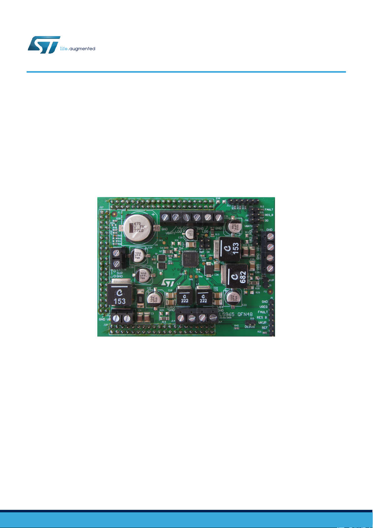
L5965 evaluation board
Introduction
L5965 is a multichannel voltage regulator specifically designed to support applications that need to fulfill functional safety
requirements as defined by Automotive Safety Integrity Level (ASIL).
It is available in VQFPN-48 package.
This document describes how to use the L5965 application board in order to check device's performance.
Please refer to the datasheet.
Figure 1. L5965 evaluation board
UM2564 - Rev 1 - June 2019
For further information contact your local STMicroelectronics sales office.
www.st.com
Page 2
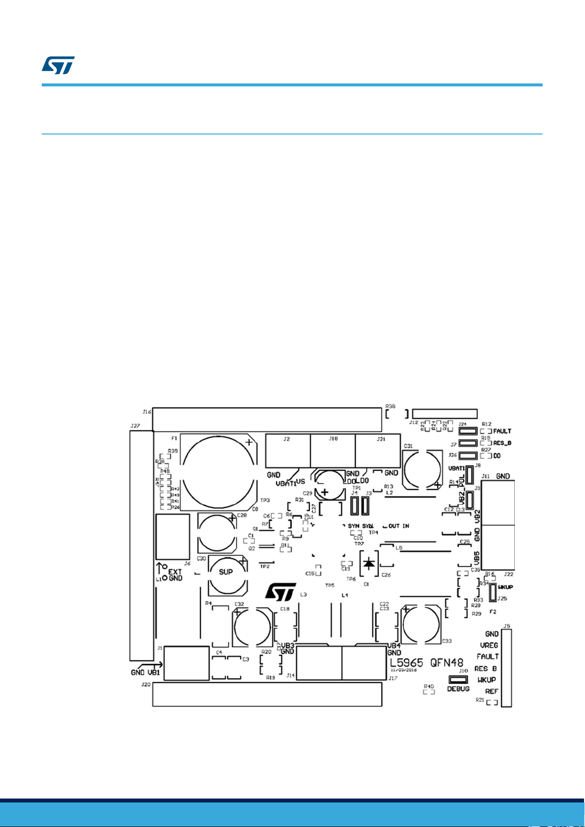
1 Board description
The demo board is an evaluation tool for L5965. L5965 embeds 1 controller and 1 buck that can both be supplied
by the car battery and used as pre-regulators, 2 buck post-regulators, 1 boost, 1 linear regulator and 1 precise
voltage reference. For further details on the device please refer to the datasheet.
Useful connectors available on the board:
• J1 = VBUCK1 (Buck1 output connector)
• J2 = VBAT1 (Battery input power supply, supplying Buck1 and Buck2)
• J3 = SYNCIN and ground pin connections
• J4 = SYNCOUT and ground pin connections
• J5 = Service/Voltage signals/VREF output connector
• J6 = EXTSUP (Alternative IC power supply connector)
• J11 = VBUCK2 (Buck2 output connector)
• J12 = SPI bus connector
• J14 = VBUCK3 (Buck3 output connector)
• J17 = VBUCK4 (Buck4 output connector)
• J18 = VSLDO LDO (Ldo input power supply connector)
• J21 = LDO (Ldo output connector)
• J22 = VBOOST (Boost output connector)
UM2564
Board description
Figure 2. Board top view design
UM2564 - Rev 1
page 2/10
Page 3

2 Board operation
The demonstration board is already set to allow the evaluation of the PMIC features. For a basic use, no
preliminary operation is necessary. Just connect a compatible voltage to the connector J2 (VBAT1) and check the
output signals on proper connectors.
Buck2, Buck3, Buck4, Boost and Vref are switched on automatically.
Buck1 and Ldo have been programmed in order to be enabled by SPI (for instruction, please read the product
datasheet, chapter 5). The Ldo input (J18) has to be connected by a wire with the output of a Buck regulator
(Buck2, for instance, on J11).
UM2564
Board operation
UM2564 - Rev 1
page 3/10
Page 4

3 Programming option
The L5965 mounted on this demonstration board is programmed as follows (see product datasheet, chapter 6.8).
Buck2 is the main regulator and provides 3.3 V at 3 A and 0.4 MHz. This is the pre-regulator that supplies the
others. Buck3 is the second regulator to switch on, and provides 2 V. Buck4 is the third regulator, supplying 1.8 V.
The fourth regulator to start is the Boost, providing 5 V and the latest one is the VREF, 3.3 V.
The reset is released after the Power Good of the main regulator (Buck2). In case of failures, the RESET_B signal
doesn’t affect the State Machine, then the regulator can still be evaluated in this condition. Also an overvoltage
cannot assert a reset. All these regulators turn on with a delay of 10 ms among them.
Buck1 and Ldo should be enabled by SPI. Once enabled, Buck1 provides 1.2 V and the Ldo supplies 1.3 V at 600
mA.
A watchdog is not required to operate the PMIC and rewriting OTP programming is forbidden.
UM2564
Programming option
Figure 3. OTP programming
UM2564 - Rev 1
page 4/10
Page 5

4 SPI connector
SPI signals are available on the J12 connector.
The SPI bus can be also used to monitor the PMIC diagnostics.
UM2564
SPI connector
Figure 4. Demo board SPI connector
UM2564 - Rev 1
page 5/10
Page 6

5 Board schematic
SYNCIN
SYNCOUT
REF
RESET _B
VREG
Debug
DO
DI
CLK
CSN
WDI
CLK
DO
CSN
REF
WKUP
WDI
RESET _B
FAULT
VREG
DI
FAULT
WKUP
C11
47nF
J9
R4
0.06R 1W 683-6580
C2 100nF
R2
0 n.m.
R8
47K
R12 100K
R23 0R
C14 2.2nF
1
2
3
4
5
6
7
J5
CONN 2.54X7
R280R
L5 6.8uH
C17
3.3uF
J3
R35
1.25K
C21
220nF
C26
3.3uF
R3
0 n.m.
C7
2.2uF 25V
C20
47nF
6
3
4
2
5
1
J12
CONN 2.54X6
R130R
1
2
J6
L3 2.2uH
C10
100nF
C5
100nF
J25
1
2
J2
C16
47nF
R140 n.m.
C4
10uF
1
2
J21
+
C29
22uF 40V
J26
C22
3.3uF
C24
100nF
C23
3.3uF
R10 20K
R15 100K
C1100nF
R22 0R
1
2
J1
C18
3.3uF
1
2
J22
R70R
R5 47K
+
C28
100uF 40V
R1
0R
J24
R190R
R24 0R
1
2
J11
1
2
J17
C12
10uF
C25
3.3uF
C9 910pF
C6
100nF
R16 10K
C27
3.3uF
C15
100nF
J10
C19
100nF
R30 1.8K
1
2
J14
+
C8
470uF 40V
R17 10K
R21 0R
L1 15uH
R27 10K
C13
10uF
DO
41
VBOOST_S
28
EXTSUP
3
VREG
4
BST1
5
GH1
6
PH1
7
GL1
8
PGND1
9
D
G
N
D
44
VREG1_S
13
COMP1
12
VBAT2
33
BST2
34
PH2
32
PGND2
31
VREG2_S
30
COMP2
29
VIN3
16
BST3
15
PH3
17
PGND3
18
PH4
22
BST4
24
VIN4
23
VREG3_S
19
VBAT1
2
A
G
N
D
46
S
GND
45
Sensen
11
SYNCIN
35
Sensep
10
SYNCOUT
36
REF
1
VSLDO
48
LDO
47
FAULT
43
WDI
37
RESET_B
42
WKUP
25
Debug
14
CSN
38
CLK
40
DI
39
P
GND
5
27
PH5
26
VREG4_S
20
PGND4
21
U1
L5965_QFN48
1
2
J18
R330R
C3
10uF
J4
GNDANA
VBUCK2
VBUCK2
VBUCK2
VBUCK2_pol
VBAT1
VBAT1
VBUCK2_pol
VBAT1
VBUCK2_pol
VBUCK1
VBUCK3
VBUCK4
VBUCK5
VBUCK2_pol
VBUCK2
VBUCK2
LDO
VBAT1
EXTSUP
EXTSUP
VBUCK1
VBAT1
SYNCIN
SYNCOUT
No Jumpe r
VBAT1
-
+
EXSUP
-
+
VSLDO
-
+
1.3V
-
+
VBUCK5 5V
-
+
VBUCK4 1.8V
-
+
VBUCK3 2V
-
+
VBUCK2 3.3V 3A
-
+
VBUCK1 1.2V
-
+
VBAT1
CSN
DI
DO
CLK
GND
Debug
WDI
REF
WKUP
RESET_B
FAULT
VREG
GND
+
C30
100uF 40V
4
1 5
6
7
8
2
3
Q1
STL11N4LLF5
4
1
5
6
7
8
2
3
Q2
STL11N4LLF5
XAL1010-153
+
C31
100uF 40V
L2 15uH
XAL1010-153
+
C32
100uF 40V
XAL7070-222
L4 2.2uH
XAL7070-222
+
C33
100uF 40V
XAL1010-682
1
F1
1
F2
1
F3
1
F4
1
TP1
PGND
C34100nF
C35100nF
PGND5
PGND5 PGND5
PGND5
PGND4 PGND4
PGND3 PGND3
PGND2 PGND2
PGND1PGND1
PGND1
PGND2
PGND3
PGND4
PGND4PGND3PGND2PGN D1
R9 0R
R11 0R
J7
1 2
D1
STPS5L60-Y
GNDANA
GNDANA
GNDANA
3.3V
UM2564
Board schematic
Figure 5. Board schematic
UM2564 - Rev 1
page 6/10
Page 7

6 Information on board use
This evaluation board/kit is intended for the following uses:
• Engineering development
• Demonstrations
• Evaluation purposes only
It is not considered by ST Microelectronics (STM) to be a finished end-product fit for general consumer use. The
people who handle the product(s) must have electronics training and must observe good engineering standard
practices.
For this reason the goods being provided are not intended to be complete in terms of required design, marketing,
and/or manufacturing-related protective considerations, including product safety and environmental measures
typically found in end products that incorporate such semiconductor components or circuit boards. This evaluation
board/kit does not fall within the purpose of the European Union directives regarding electromagnetic
compatibility, restricted substances (RoHS), recycling (WEEE), FCC, CE or UL, and therefore may not meet the
technical requirements of these directives or other related directives.
UM2564
Information on board use
UM2564 - Rev 1
page 7/10
Page 8

Revision history
UM2564
Table 1. Document revision history
Date Version Changes
17-Jun-2019 1 Initial release.
UM2564 - Rev 1
page 8/10
Page 9

UM2564
Contents
Contents
1 Board description .................................................................2
2 Board operation ...................................................................3
3 Programming option...............................................................4
4 SPI connector .....................................................................5
5 Board schematic ..................................................................6
6 Information on board use ..........................................................7
Revision history ........................................................................8
UM2564 - Rev 1
page 9/10
Page 10

UM2564
IMPORTANT NOTICE – PLEASE READ CAREFULLY
STMicroelectronics NV and its subsidiaries (“ST”) reserve the right to make changes, corrections, enhancements, modifications, and improvements to ST
products and/or to this document at any time without notice. Purchasers should obtain the latest relevant information on ST products before placing orders. ST
products are sold pursuant to ST’s terms and conditions of sale in place at the time of order acknowledgement.
Purchasers are solely responsible for the choice, selection, and use of ST products and ST assumes no liability for application assistance or the design of
Purchasers’ products.
No license, express or implied, to any intellectual property right is granted by ST herein.
Resale of ST products with provisions different from the information set forth herein shall void any warranty granted by ST for such product.
ST and the ST logo are trademarks of ST. For additional information about ST trademarks, please refer to www.st.com/trademarks. All other product or service
names are the property of their respective owners.
Information in this document supersedes and replaces information previously supplied in any prior versions of this document.
© 2019 STMicroelectronics – All rights reserved
UM2564 - Rev 1
page 10/10
 Loading...