

Multifunction voltage regulator for car radio
Features
■ Four outputs
– 8.5V @ 200mA (V8P5)
– 8/10V @ 1000mA selectable 10V or 8V
(V810)
– 3.3V @ 100mA permanent (VSTBY)
– 3.3V @ 800mA (VREGSW)
■ Two protected high side driver (HSD1, HSD2)
■ Reset function
■ Battery voltage (under/over) warning output
■ Load dump protection
■ Independent thermal shutdown on all
regulators and HSDs
■ Overcurrent limitation
■ Storage CAP output (STCAP)
■ Small CAP required by stability of regulators
■ All pins ESD protected
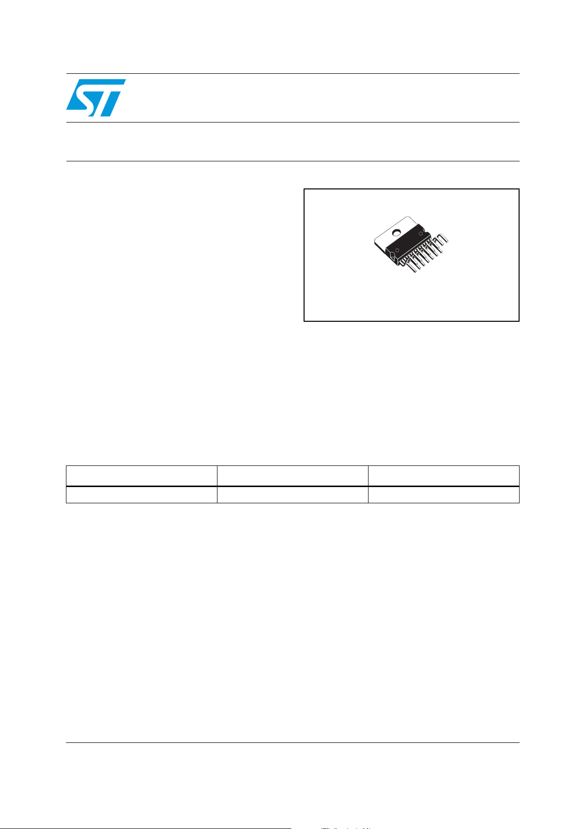
Table 1. Device summary
L5959
Multiwatt15
Description
The L5959 contains a four voltage regulator and
two protected HSDs. HSDs are protected against
loss of ground and loss of battery.
The IC includes a monitoring circuit for detection.
The IC features a very low quiescent current in
stand-by and independent thermal shutdown.
Order code Package Packing
L5959 Multiwatt15 Tube
August 2007 Rev 2 1/19
www.st.com
1

Contents L5959
Contents
1 Block diagram . . . . . . . . . . . . . . . . . . . . . . . . . . . . . . . . . . . . . . . . . . . . . . 5
2 Pins description . . . . . . . . . . . . . . . . . . . . . . . . . . . . . . . . . . . . . . . . . . . . 6
2.1 Pins connection . . . . . . . . . . . . . . . . . . . . . . . . . . . . . . . . . . . . . . . . . . . . . 6
3 Electrical specification . . . . . . . . . . . . . . . . . . . . . . . . . . . . . . . . . . . . . . . 7
3.1 Absolute maximum ratings . . . . . . . . . . . . . . . . . . . . . . . . . . . . . . . . . . . . . 7
3.2 Thermal data . . . . . . . . . . . . . . . . . . . . . . . . . . . . . . . . . . . . . . . . . . . . . . . 7
3.3 Electrical characteristics . . . . . . . . . . . . . . . . . . . . . . . . . . . . . . . . . . . . . . . 7
4 Timing diagrams . . . . . . . . . . . . . . . . . . . . . . . . . . . . . . . . . . . . . . . . . . . 13
5 Package information . . . . . . . . . . . . . . . . . . . . . . . . . . . . . . . . . . . . . . . . 17
6 Revision history . . . . . . . . . . . . . . . . . . . . . . . . . . . . . . . . . . . . . . . . . . . 18
2/19

L5959 List of tables
List of tables
Table 1. Device summary . . . . . . . . . . . . . . . . . . . . . . . . . . . . . . . . . . . . . . . . . . . . . . . . . . . . . . . . . . 1
Table 2. Enable logic . . . . . . . . . . . . . . . . . . . . . . . . . . . . . . . . . . . . . . . . . . . . . . . . . . . . . . . . . . . . . 5
Table 3. Absolute maximum ratings . . . . . . . . . . . . . . . . . . . . . . . . . . . . . . . . . . . . . . . . . . . . . . . . . . 7
Table 4. Thermal data. . . . . . . . . . . . . . . . . . . . . . . . . . . . . . . . . . . . . . . . . . . . . . . . . . . . . . . . . . . . . 7
Table 5. Electrical characteristics . . . . . . . . . . . . . . . . . . . . . . . . . . . . . . . . . . . . . . . . . . . . . . . . . . . . 7
Table 6. Document revision history . . . . . . . . . . . . . . . . . . . . . . . . . . . . . . . . . . . . . . . . . . . . . . . . . 18
3/19

List of figures L5959
List of figures
Figure 1. Block diagram . . . . . . . . . . . . . . . . . . . . . . . . . . . . . . . . . . . . . . . . . . . . . . . . . . . . . . . . . . . . 5
Figure 2. Pins connection (top view) . . . . . . . . . . . . . . . . . . . . . . . . . . . . . . . . . . . . . . . . . . . . . . . . . . 6
Figure 3. Timing diagram of regulators and HSD . . . . . . . . . . . . . . . . . . . . . . . . . . . . . . . . . . . . . . . 13
Figure 4. STCAP and RST diagram. . . . . . . . . . . . . . . . . . . . . . . . . . . . . . . . . . . . . . . . . . . . . . . . . . 13
Figure 5. VBATVW (over/under voltage warning) . . . . . . . . . . . . . . . . . . . . . . . . . . . . . . . . . . . . . . . 14
Figure 6. Independent thermal shutdown . . . . . . . . . . . . . . . . . . . . . . . . . . . . . . . . . . . . . . . . . . . . . 15
Figure 7. RST glitch rejection. . . . . . . . . . . . . . . . . . . . . . . . . . . . . . . . . . . . . . . . . . . . . . . . . . . . . . . 16
Figure 8. Enable on/off delay . . . . . . . . . . . . . . . . . . . . . . . . . . . . . . . . . . . . . . . . . . . . . . . . . . . . . . . 16
Figure 9. Multiwatt15 (vertical) mechanical data and package dimensions . . . . . . . . . . . . . . . . . . . . 17
4/19
L5959 Block diagram
1 Block diagram
Figure 1. Block diagram
VBAT
STCAP
LOAD-DUMP
Tw o H S D
V810
VSTBY
VREGSW
V8P5
HSD1
HSD2
V810
VSTBY
VREGSW
V8P5
VBATVW
RST
EN0
ENABLEEN1
EN2
Table 2. Enable logic
EN2 EN1 EN0 VREGSW V8P5 HSD1
RESET
V810
(8V)
RSTDLY
V810
(10V)
0 0 0 Off Off Off Off Off Off
0 0 1 On On On Off On On
0 1 0 On Off Off Off Off Off
0 1 1 On On On Off Off On
1 0 0 On On On Off Off Off
1 0 1 On On On Off On Off
1 1 0 On On On On Off Off
1 1 1 On On On On Off On
5/19
HSD2
Pins description L5959
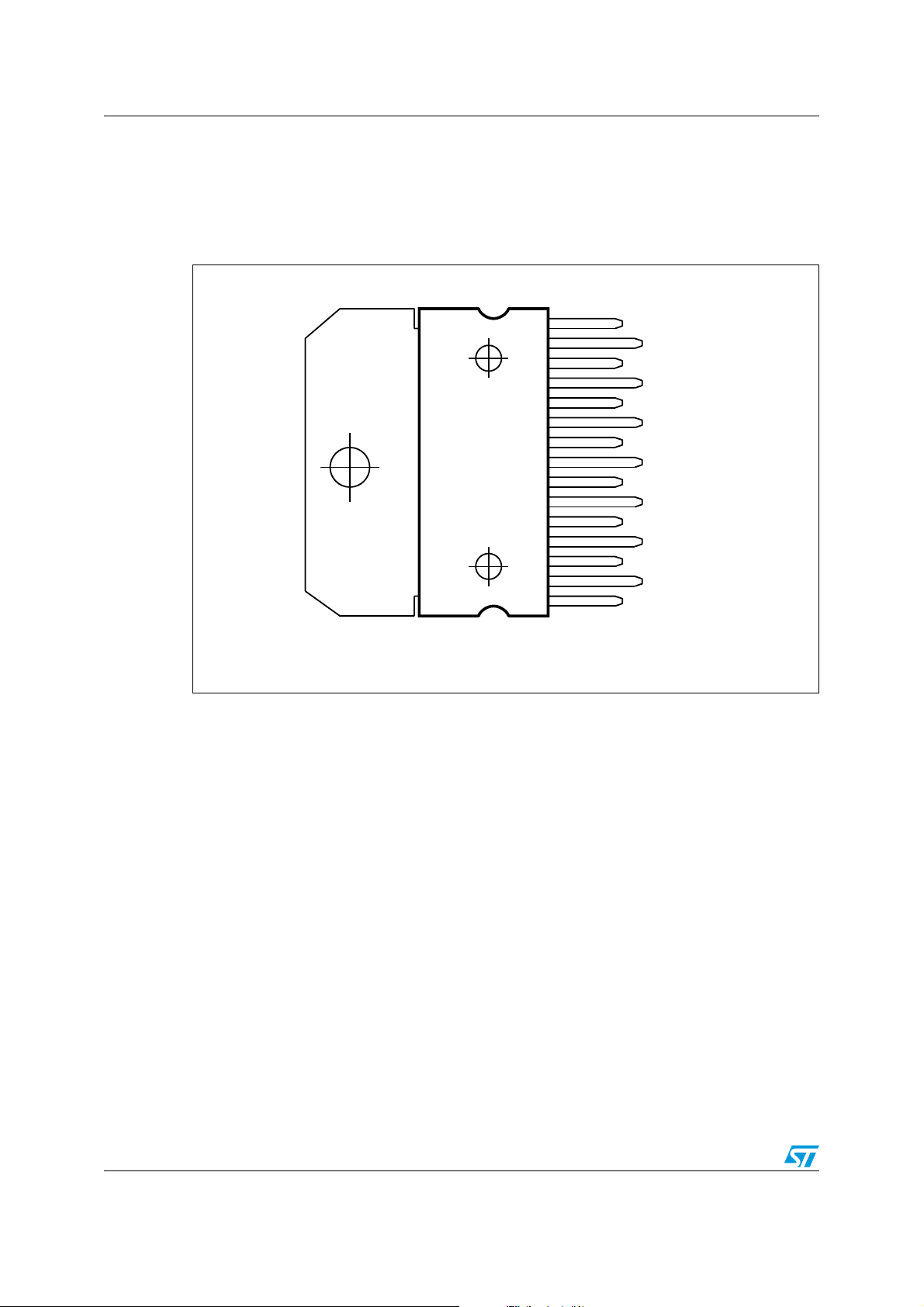
2 Pins description
2.1 Pins connection
Figure 2. Pins connection (top view)
15
14
13
12
11
10
VBAT
V810
V8P5
VREGSW
STCAP
VSTBY
9
8
7
6
5
4
3
2
1
D06AU1637
HSD1
GND
VBATVW
EN2
EN1
EN0
RSTDLY
RST
HSD2
6/19

L5959 Electrical specification
3 Electrical specification
3.1 Absolute maximum ratings
Table 3. Absolute maximum ratings
Symbol Parameter Value Unit
V
BATDC
V
BATTR
R
T
T
I
O
ESR
op
stg
T
P
j
d
DC operating supply voltage 30 V
Transient supply voltage 50 V
Output current internally limited
Output capacitor series eq. resistance (MAX.) 0.5 Ω
Operating temperature range -40 to 105 °C
Storage temperature -55 to 150 °C
Junction temperature -55 to 150 °C
Power dissipation T
= 85°C 43 W
case
3.2 Thermal data
Table 4. Thermal data
Symbol Parameter Multiwatt Unit
R
th j-case
Thermal resistance junction to case max. 1.8 °C/W
3.3 Electrical characteristics
Table 5. Electrical characteristics
Symbol Parameter Test Condition Min. Typ. Max. Unit
INPUT SUPPLIES
V
bat
V
STCAP
V
bat
V
STCAP
I
q
V
OV
V
HYSOV
(V
= 14.4V; T
S
= 25°C; unless otherwise specified)
amb
Input supply Operating 9 18 V
Input supply voltage 2 Operating 6 18 V
Battery voltage Reverse polarity non operating
Input supply voltage 2 Reverse polarity non operating
Total quiescent current
EN0 = EN1 = EN2 = 0 V;
VBAT = 14 V; I
VSTBY
= 100 µA
55 75 µA
Verify all outputs except VSTBY
VBAT Over-voltage shutdown
disabled and VBATVW*
24 27 30 V
asserted low (VBAT Rising)
Hysteresis of over-voltage
shutdown
200 750 1500 mV
7/19

Electrical specification L5959
Table 5. Electrical characteristics (continued)
(V
= 14.4V; T
S
Symbol Parameter Test Condition Min. Typ. Max. Unit
= 25°C; unless otherwise specified)
amb
V
V
HYSUV
UV
VBAT Under-voltage warning
Hysteresis of under-voltage
warning
Verify VBATVW* asserted low
(VBAT Falling)
77.47.8V
70 300 500 mV
VSTBY
(VSTBY) Output voltage of VSTBY 3.14 3.3 3.46 V
V
o
ΔV Line regulation V
ΔV
Load regulation I
i
V
over
Over shoot
PSRR Supply voltage ripple rejection
= 6 to 18V; I = 100mA -10 0 +10 mV
BAT
= 0.5 to 100 mA -40 -5 +10 mV
VSTBY
I
= 100 to 0.5 mA,
VSTBY
Co=1µF
= 50 mA;
I
VSTBY
= 20 to 1 kHz;
f
o
VBAT = 14 Vdc, 1.0 V
= 50 mA;
I
VSTBY
= 20 to 20 kHz;
f
o
VBAT = 14 Vdc, 1.0 V
50 70 dB
ac(pp)
45 55 dB
ac(pp)
2.5 6 %
Weighted filter
V
TS
V
drop
I
m
Output noise
N
Drop out voltage I
Drop out voltage I
fo = 20 Hz to 20 kHz
I
= 5 mA
VSTBY
= 100mA
VSTBY
= 5 mA 2.3 V
VSTBY
(1)
2.6 V
85 200 µV
Current limit Rshort = 0Ω 150 200 300 mA
I
= 500 µA;
VSTBY thermal shutdown
EN
VSTBY
Increase Ta until VSTBY
150 190 °C
disabled
VREGSW
V
o
(VREGSW)
V
TRK
Output voltage 3.3V 3.14 3.3 3.46 V
I
= 50 mA
VREGSW output tracking
voltage on VSTBY
VSTBY
I
VREGSW
Measure VSTBY – VREGSW
I
VSTBY
I
VREGSW
= 0.5 to 800 mA
= 0.5 mA to 100 mA
= 0.5 to 800 mA
-40 40 mV
-50 50 mV
Measure VSTBY – VREGSW
ΔV Line regulation Vin1 = 9 to 18V; I = 800mA -40 10 40 mV
ΔVi Load regulation I
VREGSW
= 1 to 800mA -50 -15 10 mV
8/19
L5959 Electrical specification
Table 5. Electrical characteristics (continued)
(V
= 14.4V; T
S
Symbol Parameter Test Condition Min. Typ. Max. Unit
= 25°C; unless otherwise specified)
amb
PSRR Supply voltage ripple rejection
I
VREGSW
fo = 20 to 1 kHz;
VBAT = 14 Vdc, 1.0 V
I
VREGSW
fo = 20 to 20 kHz;
VBAT = 14 Vdc, 1.0 V
= 400 mA;
50 70 dB
ac(pp)
= 400 mA;
45 55 dB
ac(pp)
Weighted filter
V
V
TS
V
drop
drop
I
t
don
t
doff
m
Output noise
N
Drop out voltage I
Drop out voltage I
fo = 20 Hz to 20 kHz
I
VREGSW
VREGSW
VREGSW
= 5 mA
= 800 mA 2.6 V
= 5 mA 2.3 V
85 200 µV
Current limit Rshort = 0Ω 11.52.5A
VREGSW thermal shutdown
EN
I
VREGSW
until VREGSW disabled
= 500 µA; Increase Ta
150 190 °C
Turn-on delay; Ivregsw= 5mA 10 45 110 µs
Turn-off delay, I
VREGSW
= 700 mA 45 110 µs
V8P5 (VBAT=9.5V to 18 V)
Vo (V8P5) Output voltage 8.5V 8.3 8.5 8.7 V
ΔV Line regulation VBAT = 9.5 to 18V; I = 200mA -50 3.0 50 mV
ΔVi Load regulation IV8P5 = 1 to 200mA -30 3 20 mV
= 100 mA;
I
V8P5
PSRR Supply voltage ripple rejection
= 20 to 1 kHz;
f
o
VBAT = 14 Vdc, 1.0 V
= 100 mA;
I
V8P5
= 20 to 20 kHz;
f
o
VBAT = 14 V
, 1.0 V
dc
ac(pp)
ac(pp)
50 60 dB
35 40 dB
Weighted filter
V
TS
V
drop
I
m
N
Output noise
fo = 20 Hz to 20 kHz
I
= 5 mA
V8P5
190 450 µV
Drop out voltage IV8P5 = 200mA 0.45 0.9 V
Current limit Rshort = 0Ω 275 450 700 mA
= 500 µA; Increase Ta
I
V8P5 thermal shutdown
EN
V8P5
until V8P5 disabled
150 190 °C
t
don
t
doff
V810 (8V) (V
V
o (V810)
Turn-on delay; I
Turn-off delay, I
= 9.2V to 18 V)
BAT
Output voltage 8.0V 7.6 8.0 8.4 V
ΔV Line regulation
= 5mA 10 45 110 µs
V8P5
= 200 mA 45 110 µs
V8P5
VBAT = 9.2 to 18V;
I = 1000mA
-50 3 50 mV
9/19

Electrical specification L5959
Table 5. Electrical characteristics (continued)
(V
= 14.4V; T
S
Symbol Parameter Test Condition Min. Typ. Max. Unit
= 25°C; unless otherwise specified)
amb
ΔVi Load regulation I
PSRR Supply voltage ripple rejection
= 0.5 to 1000 mA -100 -20 10 mV
V810
I
= 500 mA;
V810
fo = 20 to 1 kHz;
VBAT = 14 V
I
= 500 mA;
V810
, 1.0 V
dc
fo = 20 to 20 kHz;
VBAT = 14 V
, 1.0 V
dc
ac(pp)
ac(pp)
50 55 dB
30 35 dB
Weighted filter
V
Vdrop Drop out voltage IV810(8V) = 1000mA
I
m
TS
t
don
t
doff
V810 (10V) (V
(V810) Output Voltage 10.0V 9.5 10.0 10.5 V
V
o
ΔV Line regulation
ΔVi Load regulation I
PSRR Supply voltage ripple rejection
N
Output noise
fo = 20 Hz to 20 kHz
= 5 mA
I
V810
(1)
Current limit Rshort = 0Ω 1.5 2.3 3.5 A
V810(8v) thermal shutdown
EN
Turn-on delay; I
Turn-off delay, I
=11.2V to 18 V)
BAT
I
V810(8V)
until V810(8V) disabled
V810(8V)
V810(8V)
VBAT = 11.2 to 18V; I =
1000mA
V810
I
V810
fo = 20 to 1 kHz;
VBAT = 14 Vdc, 1.0 V
I
V810
f
o
VBAT = 14 V
= 500 µA; Increase Ta
150 190 °C
= 5mA 10 45 110 µs
= 1000 mA 45 110 µs
-50 2.5 50 mV
= 0.5 to 1000 mA -100 -25 10 mV
= 500 mA;
50 55 dB
ac(pp)
= 500 mA;
= 20 to 20 kHz;
, 1.0 V
dc
ac(pp)
30 35 dB
175 450 µV
0.45 0.9 V
Weighted filter
V
N
Output noise
fo = 20 Hz to 20 kHz
= 5 mA
I
V810
Vdrop Drop out voltage IV810(10V) = 1000mA
Current limit R
I
m
TS
t
don
t
doff
V810(10V) thermal shutdown
EN
Turn-on delay; I
Turn-off delay, I
= 0Ω 1.5 2.3 3.5 A
short
I
V810(8V)
= 500 µA; Increase Ta
until V810(10V) disabled
V810(8V)
V810(8V)
= 5mA 10 45 110 µs
= 1000 mA 45 110 µs
(1)
150 190 °C
175 450 µV
0.4 0.9 V
HIGH SIDE DRIVER1
VdropSW Drop voltage HDS1
Idc = 100mA 0.25 0.6 V
Idc = 200mA, t=5S 0.50 1.2 V
10/19

L5959 Electrical specification
Table 5. Electrical characteristics (continued)
(V
= 14.4V; T
S
Symbol Parameter Test Condition Min. Typ. Max. Unit
I
HSD1 short to ground current VHSD1=0V 240 300 400 mA
STG
I
STB
Δ
I
Q(VBAT)
TS
t
t
don
doff
t
HSD1 short to V
HSD1 bias current change
HSD1 thermal shutdown
EN
Turn-on delay; I
Turn-off delay, I
Rise time
r
HIGH SIDE DRIVER2
= 25°C; unless otherwise specified)
amb
current VHSD1=VBAT 2 10 mA
BAT
I
= 0 to 100 mA;
HSD1
Measure change in VBAT
0.15 10 mA
current
= 500 µA; Increase Ta
I
HSD1
until HSD1 disabled
= 10mA 10 50 110 µs
HSD1
= 100 mA 70 110 µs
HSD1
10% to 90%,
I
= 10mA
HSD1
150 190 °C
35 75 µs
VdropSW Drop voltage HDS2
I
HSD2 short to ground current VHSD2=0V 0.55 0.75 1 A
STG
I
STB
Δ
I
Q(VBAT)
TS
t
t
don
doff
t
HSD2 short to V
HSD2 bias current change
HSD2 thermal shutdown
EN
Turn-on delay; I
Turn-off delay, I
Rise time
r
RST (open collector output)
V
TH
V
HYS
t
rRST
t
fRST
VIH_RSTDLY
I
SRC
VSTBY reset threshold
Hysteresis of reset on rising
VSTBY
Rise time
Fall time
RSTDLY input voltage threshold Verify RST is de asserted 2.5 2.75 3.5 V
RSTDLY current RSTDLY = 0 VDC 6 8.5 12 µA
Idc = 300mA 0.2 0.6 V
Idc =450mA, t=5S 0.3 1.2 V
current VHSD2=VBAT 3.5 10 mA
BAT
I
= 0 to 300 mA;
HSD2
Measure change in VBAT
0.15 10 mA
current
IHSD2 = 500 µA; Increase Ta
until HSD2 disabled
= 10mA 10 45 110 µs
HSD2
= 300 mA 70 110 µs
HSD2
10% to 90%,
= 10mA
I
HSD2
Force VSTBY low until RST*
asserted
150 190 °C
30 75 µs
0.93 *
VSTBY
0.95 *
VSTBY
0.97 *
VSTBY
10 50 200 mV
10% to 90%,
R
= 47 kΩ,
RST
= 50 pF
C
RST
90% to 10%,R
= 50 pF
C
RST
RST
= 47 kΩ,
20 30 µs
300 1000 ns
V
11/19
Electrical specification L5959
Table 5. Electrical characteristics (continued)
(V
= 14.4V; T
S
Symbol Parameter Test Condition Min. Typ. Max. Unit
= 25°C; unless otherwise specified)
amb
T
t
por
glitch
RST POR delay time C
= 0.1 µF 20 30 50 ms
RSTDLY
Glitch rejection filter time 5 12.5 20 µs
ENABLE INPUT (VREGSW, V8P5, V810, HSD1, HSD2)
V
IH
V
V
HYSEN
I
LKGEN
1. Drop condition means that the supply voltage drop down to 100 mV from the regulated output and the regulator is sourcing
its maximal load.
2. Stability Request is design info, not tested.
Threshold recognized as high
level
Threshold recognized as low
IL
level
0.8 V
Hysteresis of enable 0.15 0.35 V
Enable input pull-down current VEN = V
to VSTBY 10 30 50 µA
IL(mIN)
2.0 V
12/19
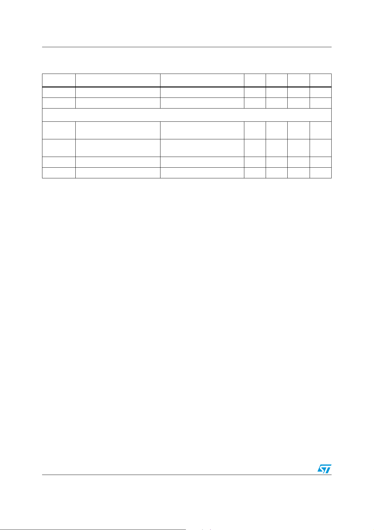
L5959 Timing diagrams
9
4 Timing diagrams
Figure 3. Timing diagram of regulators and HSD
DUMP
VBAT
VSTBY
27.4V
18V
9V
3.3V
26.6V
EN
VREGSW
V8P5
V810
HSD1
HSD2
3.3V
8.5V
8V
18V
9V
10V
9V
000 111 111000
Figure 4. STCAP and RST diagram
14V
3.3V
3.18V
3.13V
VBAT
VSTBY
AC0032
STCAP
3.3V
2.7V
t
RSTDLY
RST
AC00330
t
t
13/19

Timing diagrams L5959
Figure 5. VBATVW (over/under voltage warning)
DUMP
27.4V
18V
VBAT 14.4V
7.67V
3.3V
VBATVW
3.3V
VSTBY
3.3V
VREGSW
8.5V
V8P5
8 V
V810
27.4V
HSD1 18V
14.4V
26.6V
7.4V
27.4V
HSD2 18V
14.4V
EN
000 111
AC00331
14/19

L5959 Timing diagrams
Figure 6. Independent thermal shutdown
14.4V
VBAT
THERMAL
SHUTDOWN
(of VSTBY)
VSTBY
THERMAL
SHUTDOWN
(of VREGSW)
VREGSW
THERMAL
SHUTDOWN
(of V8P5)
V8P5
THERMAL
SHUTDOWN
(of V810)
V810
THERMAL
SHUTDOWN
(of HSD1)
ON T = 160
ON T = 160
ON T = 160
ON T = 160
ON T = 160
HSD1
THERMAL
SHUTDOWN
(of HSD2)
HSD2
EN
ON T = 160
111
AC00332
15/19
Timing diagrams L5959
Figure 7. RST glitch rejection
VSTBY
3.3V
5V
RST
Figure 8. Enable on/off delay
VERGSW
(V810, V8PS, HSDI, HSD2)
EN
000
< Tglitch
Tdon
> Tglitch
Tglitch
10%
111 000
TPOR
AC00333
Tdoff
90%
AC00334
16/19
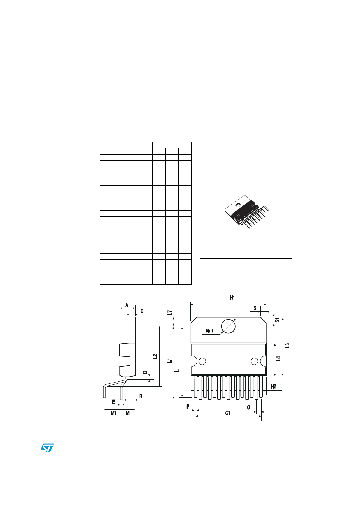
L5959 Package information
5 Package information
In order to meet environmental requirements, ST offers these devices in ECOPACK®
packages. These packages have a Lead-free second level interconnect. The category of
second Level Interconnect is marked on the package and on the inner box label, in
compliance with JEDEC Standard JESD97. The maximum ratings related to soldering
conditions are also marked on the inner box label. ECOPACK is an ST trademark.
ECOPACK specifications are available at: www.st.com.
Figure 9. Multiwatt15 (vertical) mechanical data and package dimensions
DIM.
A5 0.197
B 2.65 0.104
C 1.6 0.063
D 1 0.039
E 0.49 0.55 0.019 0.022
F 0.66 0.75 0.026 0.030
G 1.02 1.27 1.52 0.040 0.050 0.060
G1 17.53 17.78 18.03 0.690 0.700 0.710
H1 19.6 0.772
H2 20.2 0.795
L 21.9 22.2 22.5 0.862 0.874 0.886
L1 21.7 22.1 22.5 0.854 0.87 0.8 86
L2 17.65 18.1 0.695 0.713
L3 17.25 17 .5 17.75 0.679 0.689 0.699
L4 10.3 10.7 10.9 0.406 0.421 0.429
L7 2.65 2.9 0.104 0.114
M 4.25 4.55 4.85 0.167 0 .179 0.191
M1 4.73 5.08 5.43 0.186 0 .200 0.214
S 1 .9 2.6 0.075 0.102
S1 1.9 2.6 0.075 0.102
Dia1 3.65 3.85 0.144 0.152
mm inch
MIN. TYP. MAX. MIN. TYP. MAX.
OUTLINE AND
MECHANICAL DATA
Multiwatt15 (Vertical)
0016036 J
17/19

Revision history L5959
6 Revision history
Table 6. Document revision history
Date Revision Changes
26-Jun-2006 1 Initial release.
28-Aug-2007 2 Minor changes, improved quality of the drawings.
18/19

L5959
Please Read Carefully:
Information in this document is provided solely in connection with ST products. STMicroelectronics NV and its subsidiaries (“ST”) reserve the
right to make changes, corrections, modifications or improvements, to this document, and the products and services described herein at any
time, without notice.
All ST products are sold pursuant to ST’s terms and conditions of sale.
Purchasers are solely responsible for the choice, selection and use of the ST products and services described herein, and ST assumes no
liability whatsoever relating to the choice, selection or use of the ST products and services described herein.
No license, express or implied, by estoppel or otherwise, to any intellectual property rights is granted under this document. If any part of this
document refers to any third party products or services it shall not be deemed a license grant by ST for the use of such third party products
or services, or any intellectual property contained therein or considered as a warranty covering the use in any manner whatsoever of such
third party products or services or any intellectual property contained therein.
UNLESS OTHERWISE SET FORTH IN ST’S TERMS AND CONDITIONS OF SALE ST DISCLAIMS ANY EXPRESS OR IMPLIED
WARRANTY WITH RESPECT TO THE USE AND/OR SALE OF ST PRODUCTS INCLUDING WITHOUT LIMITATION IMPLIED
WARRANTIES OF MERCHANTABILITY, FITNESS FOR A PARTICULAR PURPOSE (AND THEIR EQUIVALENTS UNDER THE LAWS
OF ANY JURISDICTION), OR INFRINGEMENT OF ANY PATENT, COPYRIGHT OR OTHER INTELLECTUAL PROPERTY RIGHT.
UNLESS EXPRESSLY APPROVED IN WRITING BY AN AUTHORIZED ST REPRESENTATIVE, ST PRODUCTS ARE NOT
RECOMMENDED, AUTHORIZED OR WARRANTED FOR USE IN MILITARY, AIR CRAFT, SPACE, LIFE SAVING, OR LIFE SUSTAINING
APPLICATIONS, NOR IN PRODUCTS OR SYSTEMS WHERE FAILURE OR MALFUNCTION MAY RESULT IN PERSONAL INJURY,
DEATH, OR SEVERE PROPERTY OR ENVIRONMENTAL DAMAGE. ST PRODUCTS WHICH ARE NOT SPECIFIED AS "AUTOMOTIVE
GRADE" MAY ONLY BE USED IN AUTOMOTIVE APPLICATIONS AT USER’S OWN RISK.
Resale of ST products with provisions different from the statements and/or technical features set forth in this document shall immediately void
any warranty granted by ST for the ST product or service described herein and shall not create or extend in any manner whatsoever, any
liability of ST.
ST and the ST logo are trademarks or registered trademarks of ST in various countries.
Information in this document supersedes and replaces all information previously supplied.
The ST logo is a registered trademark of STMicroelectronics. All other names are the property of their respective owners.
© 2007 STMicroelectronics - All rights reserved
STMicroelectronics group of companies
Australia - Belgium - Brazil - Canada - China - Czech Republic - Finland - France - Germany - Hong Kong - India - Israel - Italy - Japan -
Malaysia - Malta - Morocco - Singapore - Spain - Sweden - Switzerland - United Kingdom - United States of America
www.st.com
19/19
 Loading...