

Features
■ Four outputs:
– 8.5 V @ 500 mA
– 5 V @ 300 mA Permanent
–5 V @ 800mA
– 3.3 V @ 800 mA
■ 2 A high side driver
■ Reset function
■ Ignition comparator
■ Load dump protection
■ Thermal shutdown
■ Overcurrent limitation
■ All pins ESD protected
L5957
Multifunction voltage regulator for car radio
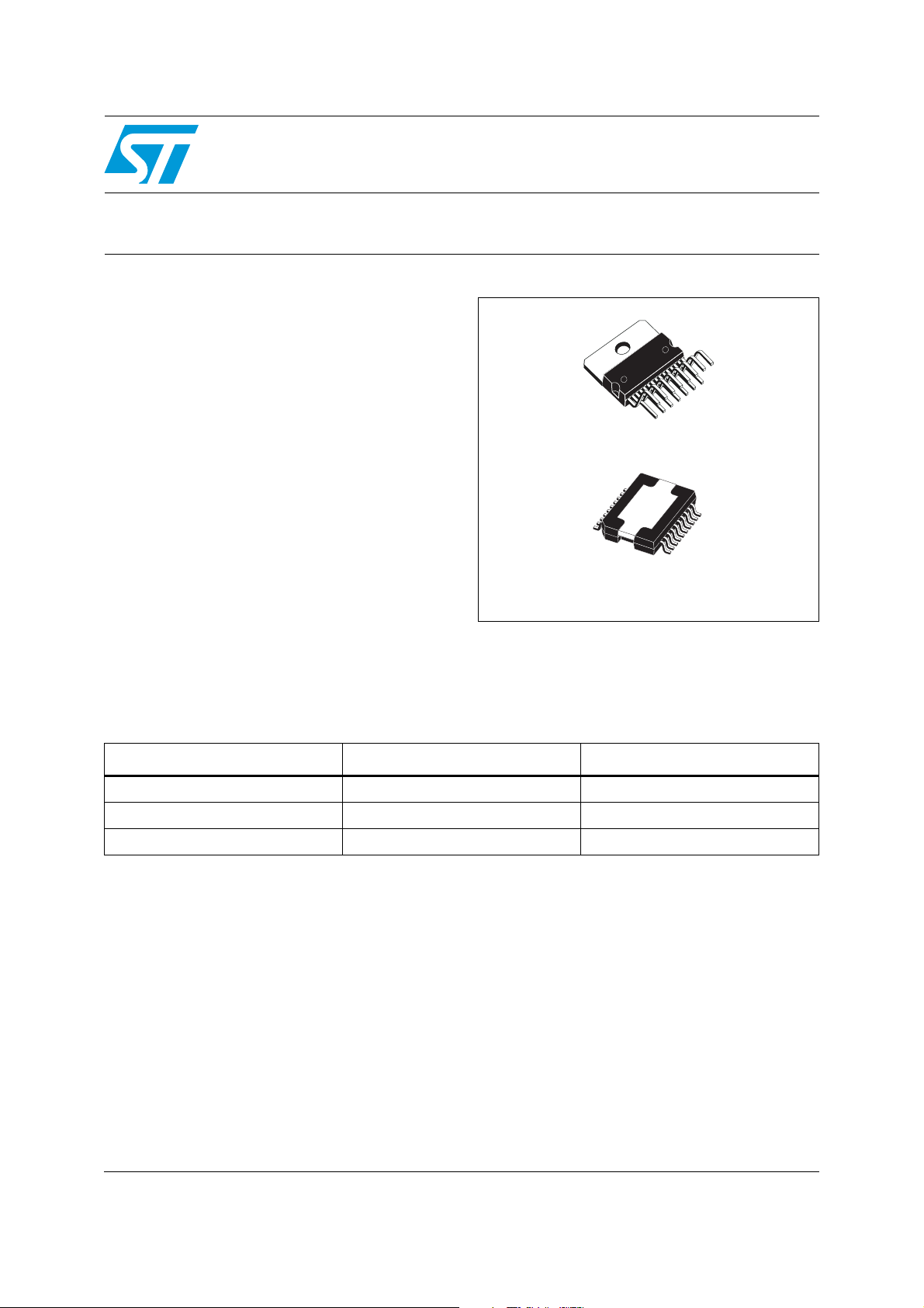
Multiwatt15 (Vertical)
PowerSO20 (Slug up)
Description
The L5957 contains a triple voltage regulator and
a power switch.
Table 1. Device summary
Order code Package Packing
L5957PD PowerSO20 (slug up) Tube
L5957PDTR PowerSO20 (slug up) Tape and reel
L5957 Multiwatt15 (Vertical) Tube
The IC includes a monitoring circuit for detection.
The IC features a very low quiescent current in
standby.
January 2010 Doc ID 14442 Rev 2 1/16
www.st.com
1

Contents L5957
Contents
1 Block and pins connection diagrams . . . . . . . . . . . . . . . . . . . . . . . . . . . 5
2 Electrical specifications . . . . . . . . . . . . . . . . . . . . . . . . . . . . . . . . . . . . . . 6
2.1 Absolute maximum ratings . . . . . . . . . . . . . . . . . . . . . . . . . . . . . . . . . . . . . 6
2.2 Thermal data . . . . . . . . . . . . . . . . . . . . . . . . . . . . . . . . . . . . . . . . . . . . . . . 6
2.3 Electrical characteristics . . . . . . . . . . . . . . . . . . . . . . . . . . . . . . . . . . . . . . . 6
3 Package information . . . . . . . . . . . . . . . . . . . . . . . . . . . . . . . . . . . . . . . . 13
4 Revision history . . . . . . . . . . . . . . . . . . . . . . . . . . . . . . . . . . . . . . . . . . . 15
2/16 Doc ID 14442 Rev 2

L5957 List of tables
List of tables
Table 1. Device summary . . . . . . . . . . . . . . . . . . . . . . . . . . . . . . . . . . . . . . . . . . . . . . . . . . . . . . . . . . 1
Table 2. Absolute maximum ratings . . . . . . . . . . . . . . . . . . . . . . . . . . . . . . . . . . . . . . . . . . . . . . . . . . 6
Table 3. Thermal data. . . . . . . . . . . . . . . . . . . . . . . . . . . . . . . . . . . . . . . . . . . . . . . . . . . . . . . . . . . . . 6
Table 4. Electrical characteristics . . . . . . . . . . . . . . . . . . . . . . . . . . . . . . . . . . . . . . . . . . . . . . . . . . . . 6
Table 5. Document revision history . . . . . . . . . . . . . . . . . . . . . . . . . . . . . . . . . . . . . . . . . . . . . . . . . 15
Doc ID 14442 Rev 2 3/16

List of figures L5957
List of figures
Figure 1. Block diagram . . . . . . . . . . . . . . . . . . . . . . . . . . . . . . . . . . . . . . . . . . . . . . . . . . . . . . . . . . . . 5
Figure 2. Pins connection . . . . . . . . . . . . . . . . . . . . . . . . . . . . . . . . . . . . . . . . . . . . . . . . . . . . . . . . . . 5
Figure 3. Typical application circuit . . . . . . . . . . . . . . . . . . . . . . . . . . . . . . . . . . . . . . . . . . . . . . . . . . . 9
Figure 4. Maximum ESR for stability valid for all the regulators outputs . . . . . . . . . . . . . . . . . . . . . . 10
Figure 5. Timing diagram of regulators and power switch . . . . . . . . . . . . . . . . . . . . . . . . . . . . . . . . . 10
Figure 6. Backup and reset diagram . . . . . . . . . . . . . . . . . . . . . . . . . . . . . . . . . . . . . . . . . . . . . . . . . 11
Figure 7. Hold and thermal protection . . . . . . . . . . . . . . . . . . . . . . . . . . . . . . . . . . . . . . . . . . . . . . . . 11
Figure 8. Ignition buffer diagram . . . . . . . . . . . . . . . . . . . . . . . . . . . . . . . . . . . . . . . . . . . . . . . . . . . . 12
Figure 9. Protection of the power switch . . . . . . . . . . . . . . . . . . . . . . . . . . . . . . . . . . . . . . . . . . . . . . 12
Figure 10. Short circuit diagram . . . . . . . . . . . . . . . . . . . . . . . . . . . . . . . . . . . . . . . . . . . . . . . . . . . . . . 12
Figure 11. PowerSO20 (slug up) mechanical data and package dimensions . . . . . . . . . . . . . . . . . . . 13
Figure 12. Multiwatt15 (vertical) mechanical data and package dimensions . . . . . . . . . . . . . . . . . . . . 14
4/16 Doc ID 14442 Rev 2
L5957 Block and pins connection diagrams
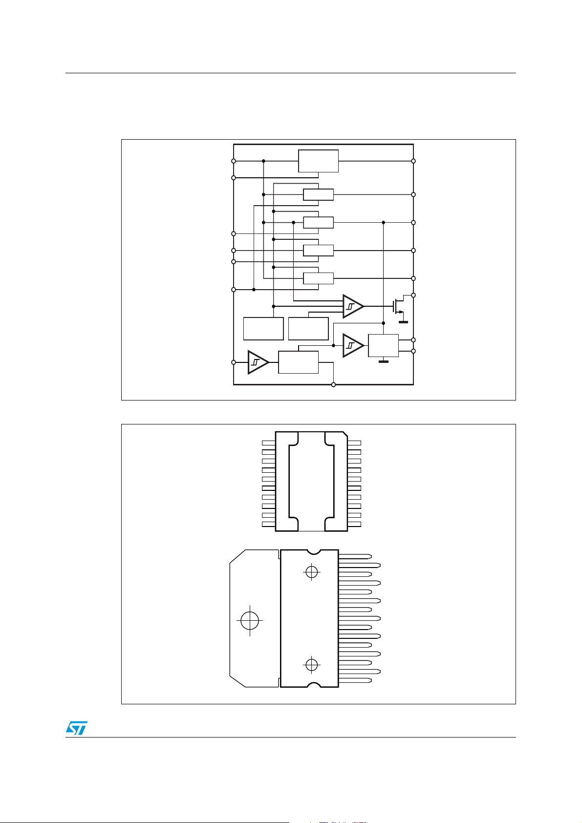
1 Block and pins connection diagrams
Figure 1. Block diagram
VINI (MAIN)
EN_SW
BU
VIN2
ENREG3(5V)
ENREG1-4(8.5V, 3.3V)
IGN
IN
Figure 2. Pins connection
THERMAL
PROTECTION
POWER
SWITCH
REG1
REG2
REG3
REG4
DUMP LOAD
PROTECTION
IGNITION
BUFFER
IGN
OUT
RESET
BUFFER
D02AU1342/L5957
SW
REG 1(8.5V)
REG 2(PERM)(5V)
REG 3(5V)
REG 4(3.3V)
HOLD
RES
CRES
N.C.
REG1(8.5V)
N.C.
VIN1
REG2(5V)
HEATSINK
SW
BU
20
19
18
17
16
15
14
13
12
11
PowerSO
D02AU1343 /L5957
Multiwatt
1
REG4(3.3V)VIN2
2
IGNINREG3(5V)
3
IGNOUT
RES
4
CRES
5
ENREG1-4(8.5V, 3.3V)
6
ENREG3(5V)
7
EN_SW
8
9
HOLD
GND
10
15
14
13
12
11
10
9
8
7
6
5
4
3
2
1
VIN2
REG3
REG1
SWITCH
BU
REG2
VIN1
GND
HOLD
EN SW
ENREG1, 4
ENREG3
CRES
RES
REG4
D03AU1513/L5957
Doc ID 14442 Rev 2 5/16

Electrical specifications L5957
2 Electrical specifications
2.1 Absolute maximum ratings
Table 2. Absolute maximum ratings
Symbol Parameter Value Unit
V
V
SDC
STR
I
T
T
P
DC operating supply voltage 30 V
Transient supply voltage 50 V
Output current internally limited
O
Operating temperature range -40 to 85 °C
op
Storage temperature -55 to 150 °C
stg
Junction temperature -55 to 150 °C
T
j
Power dissipation T
d
= 85 °C 43 W
case
2.2 Thermal data
Table 3. Thermal data
Symbol Parameter PowerSO Multiwatt Unit
R
th j-case
Thermal resistance junction-to-case Max. 1.5 1.8 °C/W
2.3 Electrical characteristics
VS = 14.4 V; T
Table 4. Electrical characteristics
= 25 °C; unless otherwise specified.
amb
Symbol Parameter Test condition Min. Typ. Max. Unit
Input supplies
V
in1
V
in2
I
q
Load Dump
V
in1
Load Dump
V
in2
Input supply voltage 1 Operating 9 - 18 V
Input supply voltage 2 Operating 6 - 18 V
Total quiescent current
Standby (-20 °C to 85 °C)
IGNIN = 5 V
REGx = 5 V, REGsw = 5 V,
IGN
= 5 V
IN
Standby (-20 °C to 85 °C)
IGN
V
in1
= 5 V, V
IN
CC
= 18 V
--70μA
-5-mA
-100- µA
18 20 22 V
Battery over voltage
V
in2
18 20 22 V
6/16 Doc ID 14442 Rev 2

L5957 Electrical specifications
Table 4. Electrical characteristics (continued)
Symbol Parameter Test condition Min. Typ. Max. Unit
Regulator 1
V
o (REG 1)
Output voltage 8.5 V - 8 8.5 9 V
ΔV Line regulation
ΔVi Load regulation I
I
q
Quiescent current I
PSRR Supply voltage ripple rejection
V
drop
I
m
Drop out voltage I
Current limit R
Regulator 2
V
o (ST BY)
Output voltage 5 V - 4.7 5 5.3 V
ΔV Line regulation
ΔVi Load regulation I
I
q
Quiescent Current I
PSRR Supply voltage ripple rejection
V
drop
I
m
Drop out voltage
Current limit R
Regulator 3
V
= 10 to 18 V; I = 500 mA - - 50 mV
in1
= 9.3 to 18 V; I = 10 mA - - 50 mV
V
in1
= 1 to 500 mA - - 100 mV
reg1
= 10 mA - - 5 mA
reg1
f = 1 kHz; V
Io = 500 mA
= 500 mA
reg1
= 0.5 Ω 0.6 - 1.2 A
short
V
= 7 to 18 V; I = 300 mA - - 50 mV
in1
= 6 to 18 V; I = 10 mA - - 50 mV
V
in1
= 1 to 300 mA - - 100 mV
reg2
= 10 mA - - 3 mA
reg2
f = 1 kHz; V
= 300 mA
I
o
I
= 300 mA
reg2
= 100 mA
I
reg2
= 0.5 Ω 400 - 800 mA
short
= 1.5 Vpp;
in1
(1)
= 1.5 Vpp;
in1
(1)
(1)
50 - - dB
--0.6V
50 - - dB
--1.5V
--0.6V
V
o (REG 3)
Output voltage 5V - 4.75 5 5.25 V
ΔV Line regulation
ΔVi Load regulation I
I
q
Quiescent current I
PSRR Supply voltage ripple rejection
V
drop
I
m
Drop out voltage I
Current limit R
Regulator 4
V
o (REG 4)
Output voltage 3.3V - 3.10 3.3 3.50 V
ΔV Line regulation V
ΔV Line regulation V
V
= 7 to 18 V; I = 800 mA - - 50 mV
in2
V
= 6 to 18 V; I = 10 mA - - 50 mV
in2
= 1 to 800 mA - - 100 mV
reg3
= 10 mA - - 5 mA
reg3
f = 1 kHz; V
Io = 800 mA
= 800 mA
reg3
= 0.5 Ω 1-2A
short
= 6 to 18 V; I = 800 mA - - 50 mV
in2
= 6 to 18 V; I = 10 mA - - 50 mV
in2
= 1.5 Vpp;
in1
(1)
50 - - dB
--1.5V
Doc ID 14442 Rev 2 7/16

Electrical specifications L5957
Table 4. Electrical characteristics (continued)
Symbol Parameter Test condition Min. Typ. Max. Unit
ΔVi Load regulation I
I
q
Quiescent current I
PSRR Supply voltage ripple rejection
V
drop
I
m
Drop out voltage I
Current limit R
= 1 to 800 mA - - 100 mV
reg4
= 10 mA - - 5 mA
reg4
f = 1 kHz; V
Io = 800 mA
= 800 mA
reg4
= 0.5 Ω 0.9 - 2 A
short
= 1.5 Vpp;
in1
(1)
48 - - dB
- - 2.65 V
Power switch
V
dropSW
I
pSW1
I
pSW2
SW
DEL
Drop voltage power switch I
= 1.8 A max. - - 0.5 V
dcSW
Peak time < 10 ms 2 - 3.5 A
Peak current power switch
Peak time > 40 ms 1 - 2 A
Delay Protection - 15 - 45 ms
Reset buffer (with push-pull buffer)
RES RES falling Vreg2 = 5 V 4.6 4.7 4.8 V
RES RES rising Vreg2 = 5 V 4.65 4.8 4.95 V
V
HYS(RES)
IH
source (RES)
IL
sink (RES)
RES
delay
Hysteresis of reset buffer - 50 - 200 mV
High level source current Reset = 0 V 1000 1300 1600 μA
Low level sink current Reset = 5 V 14 16 18 mA
Cres = 47nF - 10 - 60 ms
ΔTRES Reset rise and fall time R = 10 kΩ C = 15 pF - - 50 μs
I
Charge
I
Discharge
V
TH(F)
V
TH(R)
V
ol
V
oh
Charge current C
Discharge current C
Falling voltage threshold - 1 1.2 1.4 V
Rising voltage threshold - 2.5 2.8 3.5 V
Low level I
High level - 4.5 Vreg2 5.5 V
= 0 V 3 5 10 μA
RES
= 5 V 1 - 3 mA
RES
SINK(RES)
= 1 mA 0.3 0.5 V
Hold signal
V
lowI
V
lowh
V
lowl
V
HOLD R
V
HYS (HOLD_L)
V
HOLD F
V
HYS (HOLD_M)
output low for V
Hold output high for V
normal
Hold output low for V
Low V
threshold V
IN1
Hysteresis low TH. - 50 150 200 mV
High V
threshold V
IN1
Hysteresis high TH. - 50 150 250 mV
low Low detection - - 9 V
in1
in1
high low detection 22 - - V
in1
Normal high detection 10 - 18 V
Low TH. 9 9.5 10 V
IN1
High TH. 182022 V
IN1
Hold
8/16 Doc ID 14442 Rev 2

L5957 Electrical specifications
Table 4. Electrical characteristics (continued)
Symbol Parameter Test condition Min. Typ. Max. Unit
Ignition buffer (push-pull with schmitt trigger)
IGN
IGN
V
hys(IGNout)
IH
source(IGNout)
IL
sink(IGNout)
V
ol
V
oh
IGN
RISE
IGN
FAL L
I
CLAMP
IGN
IN
IN
IGN
IGN
out falling
out rising
Hysteresis of ignition buffer - 30 50 100 mV
High level source current I
Low level sink current I
Low level IL
High level - 4.5 Vreg2 5.5 V
Rising time C = 15 pF - - 10 μs
Fall time C = 15 pF - - 10 μs
Input clamp current VCC < V
IN
Input voltage Operative 0 - 50 V
- 1.031.171.28 V
- 1.181.271.33 V
= 0 V 1000 1500 2000 μA
GNout
= 5 V 10 15 20 mA
GNout
sink (IGNout)
= 1 mA - 0.3 0.5 V
< 50 V - - 2 mA
IGN
Enable input (regulators 1,3,4 and power switch)
V
TH
EN
IN
1. Drop condition means that the supply voltage drop down to 100 mV from the regulated output and the regulator is sourcing
its maximal load current.
Voltage threshold - 1.3 - 2.3 V
Input voltage Operative 0 - 5 V
Figure 3. Typical application circuit
Vs
470 µF
100 nF
470 µF
VIN1
EN SW
BU
VIN2
ENREG3
ENREG1-4
POWER
SWITCH
REG1
REG2
REG3
REG4
SW
REG 1
REG 2
REG 3
REG 4
HOLD
to µProcessor
to µProcessor
10 KΩ
22 µF
Cfilt (*)
Cfilt (*)
Cfilt (*)
Cfilt (*)
THERMAL
THERMAL
PROTECTION
PROTECTION
10 K
10 KΩ
IGN
IGNINIGN
IN
IN
1 nF
1 nF
(*) Recommended output filtering capacitors for all the regulators: C range = 5 µF to 100 µF, ESR range = 0.5 Ω to 10 Ω (T= -40 ˚C to +85 ˚C)
DUMP LOAD
DUMP LOAD
PROTECTION
PROTECTION
IGNITION
IGNITION
BUFFER
BUFFER
IGN
IGN
OUT
OUT
RESET
RESET
BUFFER
BUFFER
AC00427
RES
RES
CRES
CRES
to µProcessor
to µProcessor
47 nF
47 nF
Doc ID 14442 Rev 2 9/16

Electrical specifications L5957
Figure 4. Maximum ESR for stability valid for all the regulators outputs
ESR
[Ω]
10
Maximum ESR
5
Stable region
1
0.5
5
AC00591
Minimum ESR
10 100
Figure 5. Timing diagram of regulators and power switch
DUMP
VIN1=VIN2
REG1(8.5V)
REG4(3.3V)
V
9V
8.5V
3.3V
M
C [µF]
ENREG1-4
REG3(5V)
ENREG3
REG2(5V)
POWER SWITCH
EN-SW
5V
5V
V
M
9V
18V ≤ VM ≤ 22V
10/16 Doc ID 14442 Rev 2
D02AU1420A

L5957 Electrical specifications
Figure 6. Backup and reset diagram
14
4.8
4.7
5
5
3
VBATT
5V PERM
CDELAY
RESET
Figure 7. Hold and thermal protection
DUMP
22
18
VIN1
9.5
9V
8.5V
3.3V
5V
BACKUP CAP.
D02AU1422
t
t
t
HOLD
TEMPERATURE
PROTECTION
8.5V
REG1(8.5V)
REG2(5V)
REG3(5V)
3.3V
REG4(3.3V)
ENREG3
ENREG1-4
5V
5V
5V
5
ON
T≅160
D02AU1423B
Doc ID 14442 Rev 2 11/16

Electrical specifications L5957
4
Figure 8. Ignition buffer diagram
50V
IGNITION
INPUT
1.27V
1.17V
IGNITION
OUTPUT
LOAD DUMP
14V
VIN1
D02AU142
Figure 9. Protection of the power switch
V
SW
16V
Figure 10. Short circuit diagram
SHORT TO GND
REG1
REG2
REG3
REG4
SWITCH
DELAYED IN CASE
NOT
DELAYED
1.5A 3A
SHORT TO GND
SHORT TO GND
D02AU1425
SHORT TO GND
<16V
V
IN1
SHORT TO GND
I
SW
12/16 Doc ID 14442 Rev 2

L5957 Package information
3 Package information
In order to meet environmental requirements, ST offers these devices in different grades of
ECOPACK
®
packages, depending on their level of environmental compliance. ECOPACK
®
specifications, grade definitions and product status are available at: www.st.com.
ECOPACK
®
is an ST trademark.
Figure 11. PowerSO20 (slug up) mechanical data and package dimensions
DIM.
A 3.25 3.5 0.128 0.138
A2 3 3.15 3.3 0.118 0.124 0.130
A4 0.8 1 0.031 0.039
A5 0.15 0.2 0.25 0.006 0.008 0.010
a1 0.030
b 0.4 0.53 0.016 0.021
c 0.23 0.32 0.009 0.012
D (1) 15.8 16 0.622 0.630
D1 9.4 9.8 0.370 0.385
D2 1 0.039
E 13.9 14.5 0.547 0.570
E1 (1) 10.9 11.1 0.429 0.437
E2 2.9 0.114
E3 5.8 6.2 0.228 0.244
e 1.12 1.27 1.42 0.044 0.050 0.056
e3 11.43 0.450
G 0 0.1 0 0.004
H 15.5 15.9 0.61 0.625
h 1.1 0.043
L 0.8 1.1 0.031 0.043
N 10¡ (max)
R 0.6 0.024
S 0¡ (min.) 8¡ (max.)
V 5¡ (min.) 7¡ (max.)
(1) ÒD and E1Ó do not include mold flash or protusions.
- Mold flash or protusions shall not exceed 0.15mm (0.006Ó)
- Critical dimensions: ÒEÓ, Òa1Ó, ÒeÓ and ÒGÓ.
mm inch
MIN. TYP. MAX. MIN. TYP. MAX.
-0.040
0.0012
-0.0016
OUTLINE AND
MECHANICAL DATA
PowerSO20 (SLUG UP)
N
N
b
h x 45û
E2
20 11
H
A5
A
A2
e3
e
M
101
D1
D
D2 (x2)
E1
DETAIL A
Gage Plane
PSO20DME
DETAIL A
0.35
S
E3
E2
E
L
R
A4
c
V
a1
- C -
SEATING PLANE
GC
(COPLANARITY)
0088529 C
Doc ID 14442 Rev 2 13/16

Package information L5957
Figure 12. Multiwatt15 (vertical) mechanical data and package dimensions
DIM.
A5 0.197
B 2.65 0.104
C 1.6 0.063
D 1 0.039
E 0.49 0.55 0.019 0.022
F 0.66 0.75 0.026 0.030
G 1.02 1.27 1.52 0.040 0.050 0.060
G1 17.53 17.78 18.03 0.690 0.700 0.710
H1 19.6 0.772
H2 20.2 0.795
L 21.9 22.2 22.5 0.862 0.874 0.886
L1 21.7 22.1 22.5 0.854 0.87 0.886
L2 17.65 18.1 0.695 0.713
L3 17.25 17.5 17.75 0.679 0.689 0.699
L4 10.3 10.7 10.9 0.406 0.421 0.429
L7 2.65 2.9 0.104 0.114
M 4.25 4.55 4.85 0.167 0.179 0.191
M1 4.73 5.08 5.43 0.186 0.200 0.214
S 1.9 2.6 0.075 0.102
S1 1.9 2.6 0.075 0.102
Dia1 3.65 3.85 0.144 0.152
mm inch
MIN. TYP. MAX. MIN. TYP. MAX.
OUTLINE AND
MECHANICAL DATA
Multiwatt15 (vertical)
14/16 Doc ID 14442 Rev 2
0016036 J

L5957 Revision history
4 Revision history
Table 5. Document revision history
Date Revision Changes
11-Feb-2008 1 Initial release.
08-Jan-2010 2
Updated Section 1: Block and pins connection diagrams on page 5.
Updated Figure 3, 5 and 6.
Doc ID 14442 Rev 2 15/16

L5957
Please Read Carefully:
Information in this document is provided solely in connection with ST products. STMicroelectronics NV and its subsidiaries (“ST”) reserve the
right to make changes, corrections, modifications or improvements, to this document, and the products and services described herein at any
time, without notice.
All ST products are sold pursuant to ST’s terms and conditions of sale.
Purchasers are solely responsible for the choice, selection and use of the ST products and services described herein, and ST assumes no
liability whatsoever relating to the choice, selection or use of the ST products and services described herein.
No license, express or implied, by estoppel or otherwise, to any intellectual property rights is granted under this document. If any part of this
document refers to any third party products or services it shall not be deemed a license grant by ST for the use of such third party products
or services, or any intellectual property contained therein or considered as a warranty covering the use in any manner whatsoever of such
third party products or services or any intellectual property contained therein.
UNLESS OTHERWISE SET FORTH IN ST’S TERMS AND CONDITIONS OF SALE ST DISCLAIMS ANY EXPRESS OR IMPLIED
WARRANTY WITH RESPECT TO THE USE AND/OR SALE OF ST PRODUCTS INCLUDING WITHOUT LIMITATION IMPLIED
WARRANTIES OF MERCHANTABILITY, FITNESS FOR A PARTICULAR PURPOSE (AND THEIR EQUIVALENTS UNDER THE LAWS
OF ANY JURISDICTION), OR INFRINGEMENT OF ANY PATENT, COPYRIGHT OR OTHER INTELLECTUAL PROPERTY RIGHT.
UNLESS EXPRESSLY APPROVED IN WRITING BY AN AUTHORIZED ST REPRESENTATIVE, ST PRODUCTS ARE NOT
RECOMMENDED, AUTHORIZED OR WARRANTED FOR USE IN MILITARY, AIR CRAFT, SPACE, LIFE SAVING, OR LIFE SUSTAINING
APPLICATIONS, NOR IN PRODUCTS OR SYSTEMS WHERE FAILURE OR MALFUNCTION MAY RESULT IN PERSONAL INJURY,
DEATH, OR SEVERE PROPERTY OR ENVIRONMENTAL DAMAGE. ST PRODUCTS WHICH ARE NOT SPECIFIED AS "AUTOMOTIVE
GRADE" MAY ONLY BE USED IN AUTOMOTIVE APPLICATIONS AT USER’S OWN RISK.
Resale of ST products with provisions different from the statements and/or technical features set forth in this document shall immediately void
any warranty granted by ST for the ST product or service described herein and shall not create or extend in any manner whatsoever, any
liability of ST.
ST and the ST logo are trademarks or registered trademarks of ST in various countries.
Information in this document supersedes and replaces all information previously supplied.
The ST logo is a registered trademark of STMicroelectronics. All other names are the property of their respective owners.
© 2010 STMicroelectronics - All rights reserved
STMicroelectronics group of companies
Australia - Belgium - Brazil - Canada - China - Czech Republic - Finland - France - Germany - Hong Kong - India - Israel - Italy - Japan -
Malaysia - Malta - Morocco - Philippines - Singapore - Spain - Sweden - Switzerland - United Kingdom - United States of America
www.st.com
16/16 Doc ID 14442 Rev 2
 Loading...