

Multiple multifunction voltage regulator for car radio
Features
■ 2 stand-by regulators:
3.3V (125mA)
1.5V (300mA)
■ 6 regulators:
10V (40mA)
8.5V (200mA)
3.3V (850mA)
8/10V (1A)
5/3.3/1.8V (200mA)
1.8/2.5V(200mA)
■ All regulators are low dropout outputs
■ The different outputs voltage are controlled by
2
I
C Bus.
■ Reg3 on/off controlled by enable
■ Reg1, Reg2, Reg4, Reg5, Reg6 on/off
controlled by I
■ 3 high side drivers:
2A (HSD1)
0.45A (HSD2 & HSD3)
■ No external charge pump capacitors are
required
■ Stand-by mode controlled by EN pin for I
Bus and Reg1, Reg2, Reg3, Reg4, Reg5,
Reg6, HSD1, HSD2, HSD3
■ LVW function externally selectable
■ Individual thermal shutdown
Table 1. Device summary
2
CBus.
2
C
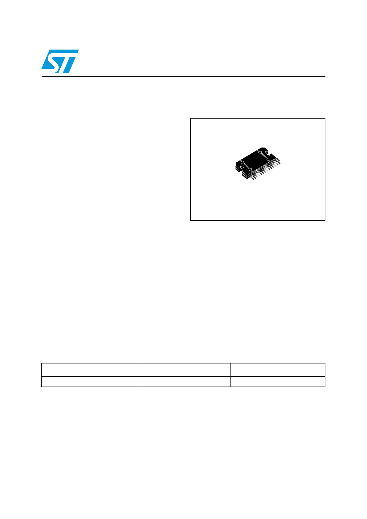
L5955
Flexiwatt27
■ Independent current limiting
■ Short circuit protection
■ Load dump protection and overvoltage
shutdown
Description
The L5955 is an integration of three high side
drivers, six regulators and two stand-by regulators
with RESET function developed to provide the
power to a complete audio system.
The outputs of the IC are controlled by I
and Enable pin.
The device is equipped with sequencing and slew
rate controls for the st-by regulators.
2
C bus
Order code Package Packing
L5955 Flexiwatt27 Tube
August 2007 Rev 1 1/17
www.st.com
17

Contents L5955
Contents
1 Block and pin connection diagrams . . . . . . . . . . . . . . . . . . . . . . . . . . . . 3
2 Electrical specification . . . . . . . . . . . . . . . . . . . . . . . . . . . . . . . . . . . . . . . 4
2.1 Absolute maximum ratings . . . . . . . . . . . . . . . . . . . . . . . . . . . . . . . . . . . . . 4
2.2 Thermal data . . . . . . . . . . . . . . . . . . . . . . . . . . . . . . . . . . . . . . . . . . . . . . . 4
2.3 Electrical characteristics . . . . . . . . . . . . . . . . . . . . . . . . . . . . . . . . . . . . . . . 4
3 Functional description . . . . . . . . . . . . . . . . . . . . . . . . . . . . . . . . . . . . . . 10
3.1 Write mode: . . . . . . . . . . . . . . . . . . . . . . . . . . . . . . . . . . . . . . . . . . . . . . . 12
3.2 Chip address byte: . . . . . . . . . . . . . . . . . . . . . . . . . . . . . . . . . . . . . . . . . . 13
3.3 Data byte: . . . . . . . . . . . . . . . . . . . . . . . . . . . . . . . . . . . . . . . . . . . . . . . . . 13
4 Package information . . . . . . . . . . . . . . . . . . . . . . . . . . . . . . . . . . . . . . . . 15
5 Revision history . . . . . . . . . . . . . . . . . . . . . . . . . . . . . . . . . . . . . . . . . . . 16
2/17
L5955 Block and pin connection diagrams
8
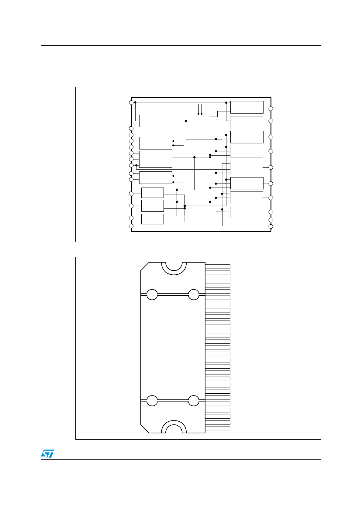
1 Block and pin connection diagrams
Figure 1. Block diagram
VBAT1
BANDGAP
VBG
CSLEW
VBAT3_1/2
MRST*
MRSTDLY
Standby Regulators
POR Logic
Vstby1
Vstby2
SDA
SCL
I2C Interface
EN
LVWIN
LVW*
HSD1
HSD2
HSD3
VBAT2
Low Voltage
Warning
High Side
High Side
Driver
Driver
High Side
High Side
Driver
Driver
High Side
Driver
VBAT1
VBGVBG
Figure 2. Pin connection (top view)
Vstby1
CSLEW
And
Sequencing
27
26
25
24
23
22
21
20
19
18
17
16
15
14
13
12
11
10
9
8
7
6
5
4
3
2
1
Vstby2
BG1
BG2
ST-By REG 3.3V
St_By REG 1.5V
10V Linear
Regulator
8.5V Linear
Regulator
3.3V Linear
Regulator
8V Linear Regulator
10V selectable
5V Linear Regulator
1.8-3.3V selectable
1.8V Linear Regulator
2.5V selectable
VSTBY1
VSTBY2
REG1
REG2
REG3
REG4
REG5
REG6
GND
PGND
TAB2
REG4
V
BAT3_2
REG3
V
BAT2
REG6
SCL
STBY2
V
BAT1
STBY1
MRST
REG5
MRSTDLY
GND
LVW
REG1
LVW_IN
REG2
Cslew
HSD3
EN
HSD2
V
BAT3_1
HSD1
PGND
SDA
TAB1
D04AU154
3/17
Electrical specification L5955
2 Electrical specification
2.1 Absolute maximum ratings
Table 2. Absolute maximum ratings
Symbol Parameter Value Unit
VS1,
VS2,
VS3_1,
VS3_2
VS1,
VS2,
VS3_1,
VS3_2
V
S1,2,3_1,3
_2,ovs
V
V
T
T
DC operating supply voltage 0.6 to 26.5 V
Transient supply over voltages, rise time = 10ms
delay time = 115ms
34 V
Overvoltage shutdown 27 V
Input voltages (EN, SDA, SCL, LVW, MRST, MRSTDLY,
in
CSLEW)
Output control voltage -0.6 to 18 V
out
Operating temperature range -40 to 85 °C
op
Storage temperature range -40 to 150 °C
stg
-0.6 to 5.5 V
2.2 Thermal data
Table 3. Thermal data
Symbol Parameter Value Unit
R
th j-case
Thermal resistance junction to case 1 °C/W
4/17
L5955 Electrical specification
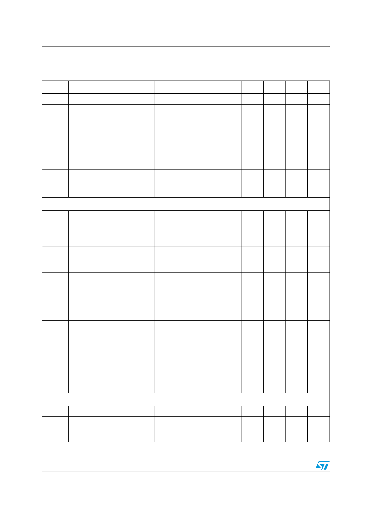
2.3 Electrical characteristics
Table 4.
Electrical characteristics
(Refer to the application circuit, V
0.5mA, I
REG1
= I
REG2
= I
REG3
= I
bat
REG4
=V
bat1+Vbat2+Vbat3
= I
REG5
= I
REG6
= 14V, I
= 5mA, R
ST-BY1
HSD1
= 0.5mA, I
= R
HSD2
= R
ST-BY2
HSD3
= 16Ω)
Symbol Parameter Test condition Min. Typ. Max. Unit
= 14V, EN = 0.
V
I
qST-BY
Stand-by quiescent current
bat
= Istby2=100uA,
I
ST-BY1
170 μA
IQ(Vbat)=Ivbat1+Ivabt2+Ivbat3
V
= 14V, EN=VSTBY1
bat
Istby1=125mA Istby2=300mA
= 40mA
I
REG1
I
I
V
V
V
L MRST
Maximum quiescent current
I
q
Enable input current V
EN
IL
Enable threshold voltage V
IH
= 200mA, I
REG2
I
= 1A, I
REG4
I
REG6
I
HSD2,3
= 14V; 5V<Enable ≥ 0V; 10
bat
= 14V;
bat
V
ST-BY1
V
ST-BY2
REG5
= 200mA, I
= 450mA
= 0.5V to VTH (ST-BY1)
= 0.5V to VTH (ST-BY2)
Rising
= 850mA
REG3
= 250mA
= 2A
HSD1
100 mA
2
0
0
0.8
0.4
0.4
MRST output voltage
V
H MRST
V
V
Falling
= VTH (ST-BY1) to 0.5V
ST-BY1
= VTH (ST-BY2) to 0.5V
ST-BY2
0
0
0.4
0.4
=
μA
V
V
V
V
V
TH MRST
t
d MRST
t
por MRST
t
f MRST
I
SCR MRST
I
LKG
MRSTDLY
V
sat
MRSTDLY
V
TH
I
LKG
V
OH
MRST output voltage threshold
Force V
ST-BY1
& V
ST-BY2
Low until MRST asserted
V
ST-BY2
· 0.93
V
ST-BY1
· 0.93
V
ST-BY2
· 0.97
V
ST-BY1
· 0.97
V
V
MRST delay time see Figure 4 13 μs
Power on reset delay time
MRST fall time
CMRSTLY = 220nF
see Figure 4
R
= 47kΩ, C
RST
RST
see Figure 4
= 50pF
20 ms
1 μs
MRSTDLY current MRSTDLY = 0 6 12 μA
MRSTDLY leakage current
MRSTDLY saturation voltage I
MRSTDLY = 5V
MRSTDLY
=0.5mA 0 0.4 V
6 μA
LVWIN input voltage threshold 1.25 V (nominal) 1.22 1.28 V
lvwin input leakage current 2 µA
V
LVW output voltage IOH=-100µA
STBY1
-0.2
V
STBY1
V
5/17
Electrical specification L5955
Table 4.
Electrical characteristics
(continued)
(Refer to the application circuit, V
0.5mA, I
REG1
= I
REG2
= I
REG3
= I
bat
REG4
=V
bat1+Vbat2+Vbat3
= I
REG5
= I
REG6
= 14V, I
= 5mA, R
ST-BY1
HSD1
= 0.5mA, I
= R
HSD2
= R
ST-BY2
HSD3
= 16Ω)
Symbol Parameter Test condition Min. Typ. Max. Unit
V
T
S HYS
3.3V/125mA V
V
ST-BY1
ΔV
LVW output voltage IOL = 100µA 0 0.2 V
OL
HSDS, REGS, V
Thermal shutdown for HSDS,
T
S
R
EGS, V
ST-BY1
, V
ST-BY2
min. load.
Increase T
REGS, V
until HSDS,
amb
ST-BY1,2
HSDS, REGS, V
Thermal shutdown hysteresis for
HSDS, REGS, V
I
CSLEW output current 7 14 µA
o
ST-BY1, ST-BY2. minimum turn
t
on
on time
ST-BY1
ST-BY1
, V
ST-BY2
Output voltage I
Line regulation
line
min. load.
Decrease T
REGS, V
=7nF; see Figure 5 1.6 ms
C
SLEW
= 125mA 3.14 3.46 V
ST-BY1
7V ≤ V
BAT
amb
ST-BY1,2
≤ 18V
until HSDS,
(Measure ΔVreg1 across V
, V
ST-BY1
Disabled
, V
ST-BY1
Disabled
ST-BY2
ST-BY2
BAT
170 °C
10 °C
10 mV
range)
ΔV
Load regulation
load
0.5mA ≤ I
(Measure ΔVreg1 across V
ST-BY1
≤ 125mA
BAT
50 mV
range)
=
Δ Quiescent current
I
q1
V
DROPOUT
I
lim1
ΔV
lead
(measure ΔI
Dropout voltage (measure V
when V
V
ST-BY1
Current limit 160 350 mA
V
absolute differential
ST-BY1
BAT
)
ST-BY1
drops 0.1V)
output voltage
ΔV
lag
SVR1 Supply voltage rejection ST-BY1
1.5V/300mA V
V
ST-BY2
ΔV
Output voltage I
Line regulation
line
ST-BY2
I
ST-BY1
I
ST-BY1
I
-
ST-BY1
BAT
I
ST-BY1
force V
V
force V
V
f
o
with 1.0Vp-p AC,
f
o
with 1.0Vp-p AC
ST-BY2
7V ≤ V
(measure Δ V
range)
= 2mA, V
= 125mA, V
BAT
= 14V,
= 14V
BAT
= 125mA
= 5mA
Low; Measure
ST-BY2
- V
ST-BY1
ST-BY1
= 120-10kHz, V
= 20-20kHz, V
ST-BY2
Low; Measure
ST-BY1
- V
ST-BY2
BAT
BAT
= 14V
= 14V
50
45
= 300mA 1.425 1.575 V
≤ 18V
BAT
ST-BY2
across V
BAT
150
10
μA
mA
2.6
1.2
2.5 V
0.25 V
dB
dB
50 mV
V
V
6/17

L5955 Electrical specification
Table 4.
Electrical characteristics
(continued)
(Refer to the application circuit, V
0.5mA, I
REG1
= I
REG2
= I
REG3
= I
bat
REG4
=V
bat1+Vbat2+Vbat3
= I
REG5
= I
REG6
= 14V, I
= 5mA, R
ST-BY1
HSD1
= 0.5mA, I
= R
HSD2
= R
ST-BY2
HSD3
= 16Ω)
Symbol Parameter Test condition Min. Typ. Max. Unit
ΔV
V
DROPOUT
I
SVR3 Supply voltage rejection ST-BY2
Load regulation 0.5mA ≤ I
load
= 300mA
Dropout voltage (measure V
V
when V
ST-BY2
Current limit 360 700 mA
lim2
ST-BY2
drops0.1V)
BAT
I
-
ST-BY2
I
ST-BY2
f
= 120-10kHz, V
o
= 5mA
with 1.0Vp-p AC,
= 20-20kHz, V
f
o
with 1.0Vp-p AC
≤ 300mA 100 mV
ST-BY2
= 14V
BAT
BAT
= 14V
50
45
4.1
3
10V/40mA REG1 output
V
REG1
ΔV
ΔV
V
DROPOUT
I
Output voltage I
Line regulation
line
Load regulation 5mA ≤ I
load
Dropout voltage (measure V
V
when V
REG1
Current limit 60 200 mA
lim1
REG1
drops 0.1V)
BAT
-
= 40mA 9.50 10 10.5 V
REG1
11.4V ≤ V
V
REG1
I
REG1
I
REG1
≤
18V (measure Δ
BAT
across V
REG1
range)
BAT
≤ 40mA 55 mV
= 40mA
= 5mA
55 mV
1200
300
Supply voltage rejection
SVR
(guaranteed by characterization-
50 dB
test at 1kHz with 50dB Limit)
=
V
V
dB
dB
mV
mV
8.5V/200mA REG2 output
V
REG2
ΔV
ΔV
V
DROPOUT
I
Output voltage I
Line regulation
line
Load regulation 5mA ≤ I
load
Dropout voltage (measure V
V
when V
REG2
Current limit 225 525 mA
lim2
REG2
Ripple rejection (guaranteed By
SVR
characterization-test at 1kHz with
50dB limit)
3.3V/850mA REG3 output
V
REG3
ΔV
ΔV
V
DROPOUT
Output voltage I
Line regulation
line
Load regulation 5mA ≤ I
load
Dropout voltage (measure V
when V
V
REG3
REG3
drops 0.1V)
BAT
BAT
drops 0.1V)
-
-
= 200mA 8.3 8.5 8.7 V
REG2
9.6V ≤ V
across V
I
REG2
I
REG2
≤ 18V (measure Δ V
BAT
range)
BAT
≤ 200mA 50 mV
REG2
REG2
= 200mA
= 5mA
50 dB
= 850mA 3.14 3.46 V
REG3
7V ≤ V
Across V
I
REG3
I
REG3
≤ 18V (Measure Δ V
BAT
range)
BAT
≤ 850mA 100 mV
REG3
REG2
= 850mA
= 5mA
50 mV
1100
600
40 mV
3.46
2.86
mV
mV
V
V
7/17

Electrical specification L5955
Table 4.
Electrical characteristics
(continued)
(Refer to the application circuit, V
0.5mA, I
REG1
= I
REG2
= I
REG3
= I
bat
REG4
=V
bat1+Vbat2+Vbat3
= I
REG5
= I
REG6
= 14V, I
= 5mA, R
ST-BY1
HSD1
= 0.5mA, I
= R
HSD2
= R
ST-BY2
HSD3
= 16Ω)
Symbol Parameter Test condition Min. Typ. Max. Unit
I
Current limit 1.25 2.5 A
lim4
Ripple rejection (guaranteed by
SVR
characterization-test at 1kHz with
50 dB
50dB Limit)
8V/10V/1A REG4 output
V
ΔV
REG4
line
Output voltage I
Line regulation
= 1A
REG4
11.4V ≤ V
V
REG4
9.3V<V
BAT
=10V
<18V For V
BAT
(measure Δ V
≤ 18V, For
REG4
across V
REG4
=8V
BAT
7.6
9.50
8.4
10.5
50
50
range)
ΔV
V
DROPOUT
I
Load regulation 5mA ≤ I
load
Dropout voltage (measure V
V
when V
REG4
Current limit 1.5 3 A
lim4
drops 0.1V)
REG4
BAT
I
-
REG4
I
REG4
≤ 1A 150 mV
REG4
= 1A
= 5mA
1.100
600
Ripple rejection (guaranteed By
SVR
characterization-test at 1kHz with
50 dB
50dB Limit)
=
V
V
mV
mV
mV
mV
1.8-3.3-5V/250mA REG5 output
V
REG5
ΔV
ΔV
V
DROPOUT
I
Output voltage I
Line regulation
line
Load regulation 5mA ≤ I
load
Dropout voltage (measure V
V
when V
REG5
Current limit 300 700 mA
lim5
drops 0.1V)
REG5
Ripple rejection (guaranteed by
SVR
characterization-test at 1kHz with
50dB limit)
BAT
-
= 250mA
REG5
7V ≤ V
≤ 18V for V
BAT
3.3V
9V<V
>18V for V
BAT
(measure Δ V
range)
REG5
I
= 250mA @ V
REG5
I
= 5mA @ V
REG5
= 250mA @ V
I
REG5
= 5mA @ V
I
REG5
I
= 250mA @ V
REG5
= 5mA @ V
I
REG5
REG5
REG5
=5V
REG5
across V
=1.8V,
BAT
1.71
3.14
4.75
1.89
3.46
5.25
40 mV
V
V
V
≤ 250mA 100 mV
REG5
REG5
REG5
REG5
REG5
REG5
=1.8V
=1.8V
=3.3V
=3.3V
=5V
=5V
4.89
4.29
3.46
2.86
1.85
1.25
V
V
V
V
V
V
50 dB
8/17

L5955 Electrical specification
Table 4.
Electrical characteristics
(continued)
(Refer to the application circuit, V
0.5mA, I
REG1
= I
REG2
= I
REG3
= I
bat
REG4
=V
bat1+Vbat2+Vbat3
= I
REG5
= I
REG6
= 14V, I
= 5mA, R
ST-BY1
HSD1
= 0.5mA, I
= R
HSD2
= R
ST-BY2
HSD3
= 16Ω)
Symbol Parameter Test condition Min. Typ. Max. Unit
1.8-2.5V/200mA REG6 output
V
REG6
ΔV
line
ΔV
load
V
DROPOUT
I
lim6
Output voltage I
Line regulation
REG6
7V ≤ V
V
REG6
= 200mA
Load regulation 5mA ≤ I
= 200mA @ V
I
REG6
I
Dropout voltage (measure V
V
REG6
when V
drops 0.1V)
REG6
BAT
-
= 5mA @ V
REG6
= 200mA @ V
I
REG6
= 5mA @ V
I
REG6
≤ 18V (measure Δ
BAT
across V
REG6
range)
BAT
≤ 200mA 50 mV
=1.8V
REG6
=1.8V
REG6
=2.5V
REG6
=2.5V
REG6
1.71
2.38
Current limit 240 600 mA
1.89
2.62
40 mV
4.89
4.29
4.22
3.62
Ripple rejection (guaranteed by
SVR
characterization-test at 1kHz with
50 dB
50dB limit)
2A HSD1
=
V
V
V
V
V
V
V
I
leak1
I
Output saturation voltage
sat
Output leakage current All Driver Outputs are Off 50 μA
Current limiting R
lim
0.45A HSD2 & HSD3
V
I
leak2,3
I
Output saturation voltage
sat
Output leakage current All driver outputs are Off 50 μA
Current limiting R
lim
Characteristics for I
V
V
V
V
LOW level input voltage 1.5 V
IL
HIGH level input voltage 3 V
IH
Input hysteresis 0.2 V
HYS
OL1
LOW level output
V
OL1
I
Input current 0.5V ≤ VI ≤ 4.5V 10 μA
1
f
SCL
SCL clock frequency 400 kHz
IHSD1 = 1A
0.6
V
continuous time operation
IHSD1=2A t=5seconds
= 0.5Ω 2.4 4 A
HSD1
IHSD2,3 = 300mA
1.2
0.6
V
V
continuous time operation
IHSD2,3=450mA t=5 seconds
= 0.5Ω 0.550 1 A
HSD2,3
2
C
Sink current = 3mA
Sink current = 6mA
1.2
0.4
0.6
V
V
V
9/17

Functional description L5955
3 Functional description
The three high side drivers are one 2A output (HSD1) and two 450mA outputs (HSD2 & 3).
The six regulator outputs are 10V at 40mA (REG1), 8.5V at 200mA (REG2), 3.3V at 850mA
(REG3), 8/10V at 1A (REG4), 1.8V/3.3V/5V at 250mA (REG5) and 1.8V/2.5V at 200mA
(REG6).
The two stand-by regulators are 3.3V at 125mA (ST-BY1) and 1.5V at 300mA (ST-BY2).
ST-BY1 and ST-BY2 are equipped with Reset function.
ST-BY1 and ST-BY2 share one Reset output (MRST).
A slew rate limiter and a sequencing function control ST-BY1 and ST-BY2 turn on/off.
The 8.5V regulator output (REG2) has a tighter tolerance output than the other regulator
outputs.
The 8.5V output is a ±2.5% (5% total range) output over temperature to improve
performance and reduce cost on the 8.5V output. The other outputs are ±5% over
temperature.
The two STAND-BY regulators are switched on/off from battery line.
The REG3 is switched on/off by Enable pin which also activate the I
The other Regulators and HSD’s are turned on/off independently by I
controls the regulators' output voltages.
2
C BUS.
2
C BUS, which also
With ENABLE pin set to 0 the total current sunk from the battery line minimized.
Figure 3. Reset and power-on reset schematic
VSTBY1
VSTBY2
FOR MRST
REG6
FOR RSTR6
1μA
5V
RESET DRIVER
(1FAULT)
I
VCP
MA
5.6pF
PULL DOWN
LATCH
SQ
FF2
R
Q
WINDOW
COMPARATOR
LATCH
SQ
FF1
R
Q
1μA
rst*
5V
MB
D02AU1401
RST*
CRSTDLY
0.22
μF
10/17

L5955 Functional description
Figure 4. Reset timing
<td MRST
<td RSTR6
VREG6
VSTBY1 or 2
MRST*
RSTR6
Figure 5. SLEW function
V
3.3V
1.5V
td MRST
td RSTR6
tf MRST
tf RSTR6
VSTBY1
VSTBY2
t
por
D02AU1402
Figure 6. Sequencing function
V
V
lead
dV
dV
t
ON
VBAT
t
t
STBY1
dV
lead
STBY2
Iag
dV
Iag
D02AU1404
t
11/17

Functional description L5955
Figure 7. Definition of timing on the I2C Bus.
SDA
t
BUP
SCL
PS P
t
HD;DAT
t
LOW
t
HD;DAT
t
R
t
HIGH
t
F
t
SU;DAT
t
SU;STA
t
HD;STA
Sr
D99AU1007
t
SP
t
SU;STO
Figure 8. Typical application circuit
V
BAT1
T.B.D.
T.B.D.
T.B.D.
STBY1
10K
V
BAT1
V
BAT2
V
BAT3_1
V
BAT3_2
EN
SCL
SDA
Cslew
MRSTDLY
0.1μF
LVW
MRST
LVW_IN
19
23
5
25
7
21
2
9
15
STBY1
18
STBY2
20
REG1
12
REG2
10
REG3
24
REG4
26
REG5
16
REG6
22
4
HSD1
6
HSD2
8
HSD3
8 x 10μF
13
GND
14
3
PGND
17
27
TAB1
1
TAB2
11
3.1 Write mode:
Chip address Data byte
S 0 A A .. .. P
MSB LSB MSB LSB
S = START condition - SDA goes from high to low while SCL is high
A = Acknowledge - the device being written to, pulls down on data line (SDA) during the
acknowledge clock pulse.
P = STOP condition - SDA goes from low to high while SCL is high.
12/17

L5955 Functional description
3.2 Chip address byte:
Table 5. Chip address byte
Chip address Read/write
A7 A6 A5 A4 A3 A2 A1 A0
0 001000 0
3.3 Data byte:
Table 6. Data byte
b7 b6 b5 b4 b3 b2 b1 b0
Data byte 0
REG6 SET REG5 SET2 REG5 SET1 REG4 SET HSD3EN HSD2EN0 HSD1EN0
Data byte 1
REG6EN REG5EN REG4EN REG2EN REG1EN
Default mode is 0000 0000 which corresponds to all outputs being off, low power mode.
Table 7. Data byte 0 description
Name Description State Definition bit
REG6 SET REG6 output voltage configuration
REG5 SET1
REG5 SET2
REG5 output voltage configuration
REG4 SET REG4 output voltage configuration
HSD3EN HSD3 Enable
HSD2EN HSD2 Enable
HSD1EN HSD1 Enable
01.8Vb7
12.5Vb7
00 5.0V b5, b6
01 3.3V b5, b6
10 1.8V b5, b6
11 x b5, b6
08.0Vb4
1 10.0V b4
0Offb2
1Onb2
0Offb1
1Onb1
0Offb0
1Onb0
13/17

Functional description L5955
Table 8. Data byte 1 description
Name Description State Definition bit
REG6 EN REG6 Enable
REG5 EN REG5 Enable
REG4 EN REG4 Enable
REG2 EN REG2 Enable
REG1 EN REG1 Enable
0Off
b6
1On
0Off
b5
1On
0Off
b4
1On
0Off
b2
1On
0Off
b1
1On
14/17

L5955 Package information
4 Package information
In order to meet environmental requirements, ST offers these devices in ECOPACK®
packages. These packages have a lead-free second level interconnect. the category of
second level interconnect is marked on the package and on the inner box label, in
compliance with JEDEC Standard JESD97. The maximum ratings related to soldering
conditions are also marked on the inner box label. ECOPACK is an ST trademark.
ECOPACK specifications are available at: www.st.com.
Figure 9. Flexiwatt27 (vertical) mechanical data and package dimensions
DIM.
A 4.45 4.50 4.65 0.175 0.177 0.183
B 1.80 1.90 2.00 0.070 0.074 0.079
C 1.40 0.055
D 0.75 0.90 1.05 0.029 0.035 0.0 41
E 0.37 0.39 0.42 0.014 0.015 0.016
F (1) 0.57 0.022
G 0.80 1.00 1.20 0.031 0.040 0.047
G1 25.75 26.00 26.25 1.014 1.023 1.033
H (2) 28.90 29.23 29.30 1.139 1.150 1.153
H1 17.00 0.669
H2 12.80 0.503
H3 0.80 0.031
L (2) 22.07 22.47 22.87 0.869 0.884 0.904
L1 18.57 18. 97 19.3 7 0.731 0.747 0.762
L2 (2) 15.50 15.70 15.90 0.610 0.618 0.626
L3 7.70 7.85 7.95 0.303 0.309 0.313
L4 5 0.197
L5 3.5 0.138
M 3.70 4.00 4.30 0.145 0.157 0.169
M1 3.60 4.00 4.40 0.142 0.157 0.173
N 2.20 0.086
O 2 0.079
R 1.70 0.067
R1 0.5 0.02
R2 0.3 0.12
R3 1.25 0.049
R4 0.50 0.019
V5˚ (Typ.)
V1 3˚ (Typ.)
V2 20˚ (Typ.)
V3 45˚ (Typ.)
(1): dam-ba r protusion not inc luded
(2): molding pr otusion includ ed
mm inch
MIN. TYP. MAX. MIN. TYP. MAX.
OUTLINE AND
MECHANICAL DATA
Flexiwatt27 (vertical)
V
C
B
H
V3
OL3 L4
L2
Pin 1
H3
G
H1
G1
H2
R3
N
F
V
A
R4
R2
R
L
L1
V2
R2
V1
R1
L5
FLEX27ME
R1 R1
M1
M
V1
D
E
7139011
15/17

Revision history L5955
5 Revision history
Table 9. Document revision history
Date Revision Changes
29-Aug-2007 1 Initial release.
16/17

L5955
Please Read Carefully:
Information in this document is provided solely in connection with ST products. STMicroelectronics NV and its subsidiaries (“ST”) reserve the
right to make changes, corrections, modifications or improvements, to this document, and the products and services described herein at any
time, without notice.
All ST products are sold pursuant to ST’s terms and conditions of sale.
Purchasers are solely responsible for the choice, selection and use of the ST products and services described herein, and ST assumes no
liability whatsoever relating to the choice, selection or use of the ST products and services described herein.
No license, express or implied, by estoppel or otherwise, to any intellectual property rights is granted under this document. If any part of this
document refers to any third party products or services it shall not be deemed a license grant by ST for the use of such third party products
or services, or any intellectual property contained therein or considered as a warranty covering the use in any manner whatsoever of such
third party products or services or any intellectual property contained therein.
UNLESS OTHERWISE SET FORTH IN ST’S TERMS AND CONDITIONS OF SALE ST DISCLAIMS ANY EXPRESS OR IMPLIED
WARRANTY WITH RESPECT TO THE USE AND/OR SALE OF ST PRODUCTS INCLUDING WITHOUT LIMITATION IMPLIED
WARRANTIES OF MERCHANTABILITY, FITNESS FOR A PARTICULAR PURPOSE (AND THEIR EQUIVALENTS UNDER THE LAWS
OF ANY JURISDICTION), OR INFRINGEMENT OF ANY PATENT, COPYRIGHT OR OTHER INTELLECTUAL PROPERTY RIGHT.
UNLESS EXPRESSLY APPROVED IN WRITING BY AN AUTHORIZED ST REPRESENTATIVE, ST PRODUCTS ARE NOT
RECOMMENDED, AUTHORIZED OR WARRANTED FOR USE IN MILITARY, AIR CRAFT, SPACE, LIFE SAVING, OR LIFE SUSTAINING
APPLICATIONS, NOR IN PRODUCTS OR SYSTEMS WHERE FAILURE OR MALFUNCTION MAY RESULT IN PERSONAL INJURY,
DEATH, OR SEVERE PROPERTY OR ENVIRONMENTAL DAMAGE. ST PRODUCTS WHICH ARE NOT SPECIFIED AS "AUTOMOTIVE
GRADE" MAY ONLY BE USED IN AUTOMOTIVE APPLICATIONS AT USER’S OWN RISK.
Resale of ST products with provisions different from the statements and/or technical features set forth in this document shall immediately void
any warranty granted by ST for the ST product or service described herein and shall not create or extend in any manner whatsoever, any
liability of ST.
ST and the ST logo are trademarks or registered trademarks of ST in various countries.
Information in this document supersedes and replaces all information previously supplied.
The ST logo is a registered trademark of STMicroelectronics. All other names are the property of their respective owners.
© 2007 STMicroelectronics - All rights reserved
STMicroelectronics group of companies
Australia - Belgium - Brazil - Canada - China - Czech Republic - Finland - France - Germany - Hong Kong - India - Israel - Italy - Japan -
Malaysia - Malta - Morocco - Singapore - Spain - Sweden - Switzerland - United Kingdom - United States of America
www.st.com
17/17
 Loading...