

L5951
TRIPLE OUTPUT MULTIFUNCTION VOLTAGE REGULATOR
FOR CAR RADIO WITH IDR/CLASS 2 INTERFACE
■
3 VOLTAGE REGULATORS:
3.3V (100mA) STANDBY REGULATOR
5V (100mA) STANDBY REGULATOR
7.8V (100mA)
■
OUT OF REGULATION DETECTION FOR 5VSTANDBY REGULATO R
■
WIDE OPERATING SUPPLY VOLTAGE
RANGE FROM 4.5V UP TO 26.5V FOR
TRANSIENT 34V
■
VERY LOW STANDBY QUIESCENT
CURRENT (<150µA)
■
INPUT TO OUTPU T SIGNAL T RANS FER
FUNCTION PROGRAMM AB LE
■
LVS FUNCTION
■
TTL AND CMOS COMPATIBLE INPUTS
■
OUTPUT CURRENT LIMITATION
■
CONTROLLED OUTPUT SLOPE FOR LOW
EMI
■
OVERTEMPERATURE SHUT-DOWN
■
ABLE TO SURVIVE UNDER LOSS OF
ORDERING NUMBER: L5951
GROUND OR BATTERY
■
ESD PROTECTED
DESCRIPTION
The L5951 is a monolithic triple regulator integrated
with a SAE J1850 Integrated Driver / Receiver realized in advanced Multipower-BCD technology. It is
intended to drive single wire J1850 communications,
and offer microcontroller power and power management for automotive or industrial applications.
SO24
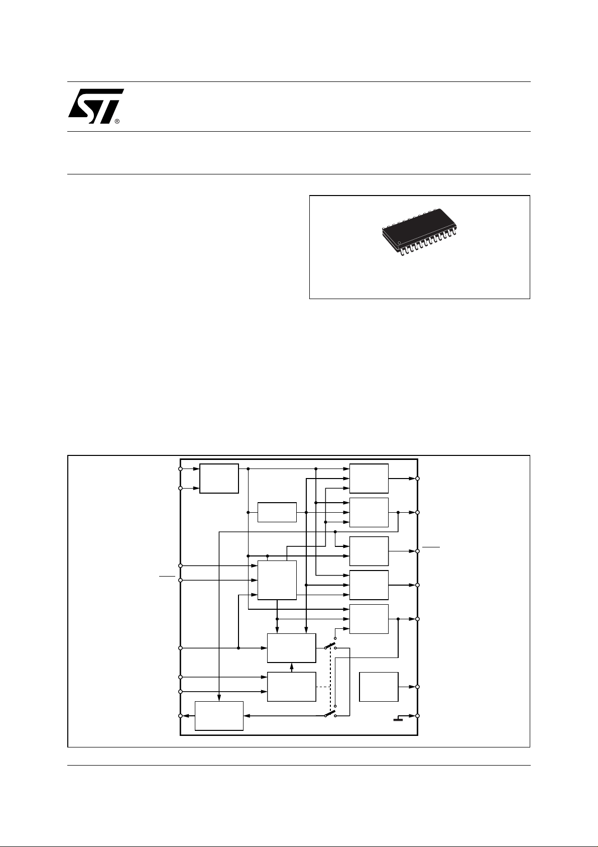
BLOCK DIAGRAM
VBAT
LVS
SLEEP
LOOP
EN
TX
4X
RX
SUPPLY
SELECTOR
DIGITAL OUTPUT
DRIVER
BANDGAP
REFERENCE
ENABLE/
PROTECTION
LOGIC
WAVESHAPING
FILTER
4XEN AND
LOOPBACK
3V
STANDBY
5V
STANDBY
RESET
7.8V
BUS DRIVER
LOSS
OF GND
PROTECTION
REG1
REG2
RESET
REG3
BUS
LOAD
GND
D99AU991
January 2001
1/13

L5951
1 FUNCTIONAL DESCRIPTION
1.1 General Features
The L5951 is an integrated circuit which provides a J1850 physical layer as well three voltage regulators. The
L5951 was developed to provide the power and Class 2/IDR interface for a microcontroller.
1.2 REG1 Outp ut Voltage
The REG1 regulator output is equal to 3.3V. The 3.3V regula tor i s non low drop out and can handl e cur rents up
to 100mA with short citcuit limit of 280mA.
1.3 REG2 Outp ut Voltage
The REG2 regulator output is equal to 5V and can handle curr ents up to 100mA with short c itcuit limit of 280mA.
The output stage of the 5V regulator is low dropout.
1.4 REG3 Outp ut Voltage
The REG3 regulator output is equal to 7.8V and can handle currents up to 100mA with short citcuit limit of
280mA. The output stage of the 7.8V regulator is low dropout. REG3 regulator is controlled by the EN (enable)
pin of the IC. REG3 can be turned on and off by toggling the EN pin. A logic "1" on the EN pin enables REG3,
while a logic "0" on the EN pin disables REG3. The maximum voltage when REG3 is off must be less than 0.2V.
Sleep* Input -
is above 2VDC, the transmitter is enabled. If the Sleep* pin drops below 0.8VDC, and EN is "0" the transceiver
goes into a low power mode. In low power mode, REG3 and the transceiver are disabled. The L5951 will still
receive messages and send them to the microcontroller out of the RX pin.
LVS input -
thermal shutdown at high voltage. For this reason a sec ondary low voltage s upply (LV S) can be used to r educe
power dissipation.
Reset* Output -
REG2 drops 0.3VDC below its normal operating voltage, the Reset* pin will go to a logic "0". Between the voltage levels of 4.65VDC (min) and 5.10VDC (max) on REG2, a reset will occur. There is a hysterisis of 50mV on
the Reset* pin.
Low Input Voltage Operation -
ready for the return of normal voltage battery levels. The L5951 will be able to retrieve data off the BUS and
send it to the micrprocessor when the supply voltage is as low as 4.9V. The regulators should stay the same
voltage as the battery voltage down to 7.0V minus operati ng headroom for the 7.8V regulator . BUS V
not guaranteed over all conditions below VBAT = 9.0V.
Waveshaping -
The digital signal is rounded at the switching points in order to reduce EMI emissions. A second order function,
I = C*dV/dt, is used to control the rise and fall times of the transmission. The rise and fall times are controlled
by an external resistor Rext . The waveshaping circuit can be enabled and disabled by the 4X pin. A logic "1"
will disable the waveshape circuit and a logic "0" will enable the waveshape circuit. In 4X mode, the speed of
the BUS is increased by a factor of four . Any signal coming from the microcontroller and going to the BUS must
be waveshaped. If loopback(LOOP) is enabled, the signal coming from the micro through the TX pin is routed
to the RX pin back to the micro with or without it being waveshaped. A logic "1" enabl es loop back and a logi c"0"
disables loopback.
Nodes -
waveforms and transmi ts a digital level signal back to a l ogic IC. The trans mitter can drive up to 32 remote transceivers. These remote nodes may be at ground potentials that ar e ±2 VDC, with respect to the assembly. Under
this condition, waveshaping will only be maintained during 3 of the 4 corners. The L5951 is a remote node on
the Class 2/IDR Bus. Each remote transcei ver has a 470 + 10% pF c apacitor on its output for EMI suppression,
The Class 2 transmitter can be turned on and turned off by the Sleep* pin. Once the voltage level
* denote s ac tive low
Reg1 and Reg2 are supplied by Vbat pin. The device could then dissipate a lot of power, causing
The L5951 has low voltage or no voltage circuitry that is a warning to the microcontroller. If
* denote s ac tive low
If battery voltage level drops below 7.0V, the outputs are to remain alive and
are
OH,min
Messages sent by the microcontroller to the transceiver are routed to a waveshaping circuit.
The transmitter provides a wave-shaped 0 to 7.7 VDC waveform on the BUS output. It also receives
2/13
L5951
as well as a 10.6 kW + 5% pull down resistor to ground. The main node has a 3,300 + 10% pF capacitor on its
output for EMI suppression, as well as a 1.5 k
there is no pr imary node , all nodes will have the 470 ±10% pF cap acitor and the 10.6k
No matter how many remote nodes are on the Class 2/IDR Bus, the RC of the Class 2/IDR Bus is maintained
at approximately 5ms. The minimum and maximum load on the Class 2/IDR Bus is given below :
Minimum Nodes (3.33 · .9) + (.47 · .9) = 3.39 nF (1.5 · 1.05) || (10.6 · 1.05) = 1.38 kΩ
Maximum Nodes (3.3 · 1.1) + 25·(0.47 · 1.1) = 16.55 nF (1.5 · 0.95) || (10.6 · 0.95) / 25 = 314Ω
1.5 Protection
The L5951 can survive under the following conditions: shorting the outputs to BAT and GND, loss of BAT, loss
of IC GND, double battery(+26.5V), 4000V ESD, 34V load dump. L5951 will not handle a reverse battery condition. External components must be implemented for reverse battery protection.
Thermal Shutdown:
thermal shutdown is broken down into two areas; V1 and V2 ouputs, and the other is V3
output and the Class 2 Bus Driver. V1 and V2 outputs shutdown at 160°C and returns to normal operation at
130°C. The V3 output and Class 2 Bus Driver shutdown at 150°C and return to normal operation at 120°C.
Current Limiting:
each voltage regulator w ill contain its ow n current prote ction, and the max imum al lowable cur -
rent for all three regulators is 280mA.
Short Circuit:
If the outputs are short circuited, the IC will begin current limi ting and eventually the thermal shut-
down will kick in. Current limiting will not disable the outputs.
Overvoltage:
The IC will not operate if the BAT voltage reaches 30V or above. V1 and V2 will not be shutdown,
but all other outputs will not operate.
Loss of Ground & Loss of Battery Connection:
Ω
+ 5% pull down resistor to ground. With more than 26 nodes
Ω ±
5% pull down resistor.
Capacitance Resistance to Ground
in this conditions a very small leakage on BUS is generated.
1.6 Protocol Description
The L5951 uses a Variable Pulse Width (VPW) modulated protocol. One frame consists of an entire message
not containing more than 12 bytes. The first bi t of each byte w ill b e the most sign ificant bi t (MSB). A transm itted
message begins with a SOF signal and ends with the EOF signal.
The data to be transmitted has to be in a specific format as follows:
idle,SOF,DATA, CRC, EOD , NB, IFR, EOF, IFS, idle
Definitions below:
idle: Logic level low on communication bus
SOF: Start of Frame
DATA: Data Bytes
CRC: Cyclic Redundancy Check Error Detection Byte
EOD: End of DATA(only when IFR is used)
NB: Normalization Bit
IFR: In-Frame Response Byte(s)
EOF: End of Frame
IFS: Inter-Frame Separation
BRK: Break(can occur on network at any time)
Idle -
Logic level low on bus any time after IFS.
Start of Frame (SOF) -
The SOF signals the receiver that a new frame is beginning. SOF signal is a logic level
3/13
L5951
high pulse identified by a pulse width of about t = 200µs.
DATA Cyclic Redundancy Check (CRC) -
sage transmitted. If an invalid CRC number is detected, then an error will be detected. The SOF signal is not
used to determine the CRC. All bits in the CRC are initially "ones" to avoid confusion with a data stream that are
all "zeros".
End of Data (EOD) -
sender of the frame w ill expect one or mor e bytes in the IFR fol lowing the E OD. If th ere is no IFR used, then the
bus would stay in a logic level low state resulting in a EOF. EOD signal is recognized by a logic level low pulse
for a duration of about 200
Normalization Bit (NB) -
the the IFR is passive, therefore it is necessary to have a signal that follows EOD. There are two forms to the
NB. First of all, the NB is a logic level high pulse. The two forms are distinguished by thier pulse widths. The first
form has a pulse width of about 64
longer pulse width of about 128
manipulate the NB to any of the two methods.
In-Frame Response (IFR) -
EOD. If the IFR stays at a logic level low for a period of time then the frame must be consider ed to be com plete.
IFR bytes can be used to send a signal back to the originator indicating the correct CRC number to confirm the
correct message was sent.
End of Frame (EOF) -
level low state for a period of time indicating the end of the frame. EOF signal is recognized by a low pulse for
a width of about 280
Inter-Frame Separation (IFS) -
Total number of bytes that can be transmitted (from SOF to EOF) is 12 bytes.
A method for determining if the message receiv ed is the same as the mes-
Used to signal the receiver about the end of data tr ans missi on. If there i s a IRF signal , the
µ
s.
The sole reason for the NB is to define the start of the in-frame r esponse. The fi rst bit
µ
s and indicates if the IFR contains a CRC or not. The second form has a
µ
s and also indicates if there is a CRC in the IFR or not. The manufacturer can
Response bytes are sent by the receiver of the transmission and start after the
Indicates the end of a frame. Once the last byte is transmitted, the bus will be in a logic
µ
s.
IFS is used to synchronize the receivers at various nodes.
ABSOLUTE MAXIMUM RATINGS
Symbol Parameter Value Unit
V
V
V
DIAG
V
IN
OUT
V
T
op
T
stg
DC Operating Supply Voltage -0.6 to 26.5 V
S
Diagnostic output voltage -0.6 to 5.5 V
Input Control Voltage (EN, Sleep, 4X, Loop, TX) -0.6 to 5.5 V
Output Control Voltage (Reset *) -0.3 to 5.5 V
Peak Supply Voltage t = 50ms 34 V
S
Operating Temperature Range -40 to 85 °C
Storage Temperature Range -40 to 150 °C
* denote s ac tive low
THERMAL DATA
Symbol Parameter Value Unit
R
th j-amb
(*) With 6cm2 on board heat sink are a.
Thermal resistance junction to ambient (*) 50 °C/W
4/13

PIN CONNECTION
L5951
REG1
RESET
REXT
GND_REG
GND_TX
GND_TX
GND_TX
GND_TX
SLEEP BUS
EN LOAD
4X TX11 14
2
3
4
5
6
7
8
9
10
D99AU992
PIN FUNCTIONS
N. Name Function
1 REG1 Regulator #1
2 Reset * Reset Output to µC
24
23
22
21
20
19
18
17
16
15
1312LOOP RX
LVS1
REG2
REG3
BAT
GND_TX
GND_TX
GND_TX
GND_TX
3 Rext Waveshaping Resistor
4 GND_REG Regulator Ground
,6,7,8,17,
GND_TX Transceiver Ground
18,19,20
9 Sleep * Transceiver Enable Input
0 EN Enable for Regulator #3
11 4X 4XBus mode (41.6K Baud)
12 LOOP Loopback Enable
13 RX Serial Data Output to mC
14 TX Serial Data Input from mC
15 Load External Pull Down to Gnd
16 Bus Bus Output to Vehicle
21 Bat Battery Supply
22 REG3 Regulator #3
23 REG2 Regulator #2
24 LVS Low Voltage Supply
*denot es active low for Sleep and Reset.
5/13

L5951
ELECTRICAL CHARACTERISTICS
(T
= 25°C, V
amb
Symbol Parameter Test Condition Min. Typ. Max. Unit
= 14.4V unless otherwise specified. Standard Loads: I
BAT
REG1
= 0.5mA, I
REG2
= 0.5mA, I
REG3
= 5mA)
I
q,ST-BY
Standby Quiescent Current EN, Sleep* = 0V, V
Maximum QuiescentCurrent V
BAT
Maximum QuiescentCurrent LVS
EN Switch Input Current V
V
ENL, ENH
V
RES, L
V
V
RES, HYS
(*) Denotes acti ve l ow.
EN Input Threshold Voltage V
Reset* Output Low Voltage Set V
Reset* Output Voltage Threshold Decrease V
RES
Reset Threshold Hysteresis 50 mV
I
= 50mA, I
REG2
EN, Sleep* = 0V, V
I
= 500µA, I
REG2
V
= 14V, I
BAT
I
= 100mA, I
REG2
I
= 30mA LVS = 0V
BUS
V
= 14V, I
BAT
I
= 100mA, I
REG2
I
= 30mA LVS = 10V
BUS
= 14V, EN ≥ 2V
BAT
V
= 14V, EN ≥ 0.8V
BAT
= 14V, VIL
BAT
V
= 14V, VIH
BAT
so V
BAT
BAT
= 50mA
REG1
BAT
= 250mA
REG1
= 100mA,
REG1
REG3
= 100mA,
REG1
REG3
drops 0.30V 0 0.02 0.4 V
REG2
so V
BAT
REG2
until Reset* drops
= 14V,
= 14V,
= 100mA,
LVS = 10V
= 100mA,
drops
350
110
10
10.5
µA
µA
mA
mA
750 µA
0
0
µA
µA
0.8 V
2
V
REG2
V
- 0.20
3.3V/100mA DC Characteristics for Regulator Output 1
V
REG1
∆V
∆V
V
DROPOUT
I
SVR1 Reg1 Supply Voltage Rejection I
5V/100mA Regulator Output 2
V
REG2
∆V
Output Voltage I
Line Regulation 7V ≤ V
line
=100mA 3.14 3.3 3.46 V
REG1
≤ 26V
BAT
(Measure ∆V
REG1
Range)
Load Regulation 0.5mA ≤ I
load
(Measure ∆V
REG1
REG1
Range)
Dropout Voltage (Measure V
V
when V
REG1
Current Limit 200 mA
lim1
drops 0.1V)
REG1
BAT
-
I
REG1
I
REG1
REG1
= 100mA
= 5mA
= I
REG2
= I
f = 20 to 20kHz
VBAT = 14Vdc, 1Vac,pp
Output Voltage I
Line Regulation 7V ≤ V
line
=100mA 4.75 5 5.25 V
REG2
≤ 26V
BAT
(Measure ∆V
REG2
Range)
Across V
≤ 100mA
Across V
= 50mA
REG3
Across V
BAT
LOAD
BAT
715mV
850mV
1
0.12
2.2
1.5
V
V
45 dB
640mV
6/13

L5951
ELECTRICAL CHARACTERISTICS
(T
= 25°C, V
amb
= 14.4V unless otherwise specified. Standard Loads: I
BAT
(continued)
REG1
= 0.5mA, I
REG2
= 0.5mA, I
REG3
= 5mA)
Symbol Parameter Test Condition Min. Typ. Max. Unit
∆V
Load Regulation 0.5mA ≤ I
load
(Measure ∆V
REG2
≤ 100mA
Across V
REG2
LOAD
14 100 mV
Range)
V
DROPOUT
I
SVR2 Reg2 Supply Voltage Rejection I
Dropout Voltage (Measure V
V
when V
REG2
Current Limit 200 mA
lim2
drops 0.1V)
REG2
BAT
-
I
REG2
I
REG2
REG1
=100mA
=5mA
= I
REG2
= I
REG3
= 50mA
450
22
45 dB
f = 20 to 20kHz
VBAT = 14Vdc, 1Vac,pp
7.8V/100mA Regulator Output 3
V
REG3
Output Voltage I
=100mA - 8.8V ≤ V
REG3
BA T
≤
7.60 7.8 8 V
Range
DV
Line Regulation 8.8V ≤ V
line
(Measure ∆V
BAT
≤ 26V
REG3
Across V
BAT
50 mV
Range)
DV
Load Regulation 5mA ≤ I
load
(Measure ∆V
REG3
≤ 100mA
Across V
REG3
LOAD
50 mV
Range)
mV
mV
V
DROPOUT
I
Dropout Voltage
(Measure V
V
drops 0.1V)
REG3
Current Limit 200 mA
lim3
BAT
- V
REG3
when
SVR3 Reg3 Supply Voltage Rejection I
I
REG3
I
REG3
REG1
= 100mA
= 5mA
= I
REG2
f = 20 to 20kHz
VBAT = 14Vdc, 1Vac,pp
DC Characteristics for Class 2 Transceiver
Standard Loads: I
BUS
BUS
BUS
BUS Guaranteed
ih
Input Voltages
il
BUS Hysteresis BUS
Hyst
REG1
= 0.5mA, I
REG2
= 0.5mA, I
Verify RX > 3 VDC
Verify RX < 3 VDC
REG3
Itoh
= 5mA
- BUS
BUSov BUS Output Voltage TX = 5 VDC,
BUS = 257 to 1380Ω to gnd
- 8.2 to 16 VDC
V
BAT
V
- 6.0 to 8.2 VDC
BAT
TX = 0V
I
BUSshort
BUS Short Circuit Current TX = 5VDC
BUS = -2 to 4.8VDC
I
BUSleak
BUS Leakage Current BUS = -2 to 0 VDC
BUS = 0 to V
= I
BAT
hhtol
REG3
= 50mA
0.5
0.04
45 dB
4.25 3.7
0.15 V
7.2
5
170 mA
0
0
3.50
V
V
V
V
V
V
mA
mA
LOAD
Load Output I
ON
= 6mA 0.045 V
LOAD
7/13

L5951
ELECTRICAL CHARACTERISTICS
(T
= 25°C, V
amb
= 14.4V unless otherwise specified. Standard Loads: I
BAT
(continued)
REG1
= 0.5mA, I
REG2
= 0.5mA, I
REG3
= 5mA)
Symbol Parameter Test Condition Min. Typ. Max. Unit
LOAD
I
BUSloss
I
LOADloss
TX
TX
I
TXVIL
I
TXVIH
4
4
I
4Xvih
I
4Xvil
L
L
I
I
Load Output (Unpowered) V
Dio
BUS & LOADCurrent during loss
of assembly V
BAT
or GND
= 0V, I
BAT
I
= 0mA,
VBAT
BUS = -18 to 9VDC
LOAD = -18 to 0 VDC
TX Input Voltage Verify BUS < 3.875VDC
VIL
VIH
Verify BUS > 3.875VDC 2
TX Input Current TX = 5VDC
TX = 0VDC
4X Input Trip Point Voltages Normal Mode
Trip 1
Trip 2
4X Mode
4X Input Current 4X = 5 VDC
4X = 0 VDC
LOOP Input Trip Point Voltages Normal Mode
Trip 1
Trip 2
LOOP Input Current LOOP = 5VDC
Lvih
Lvil
Loopback Mode 2
LOOP = 0VDC
= 6mA 0.7 V
LOAD
11
39
110
0
1.4 V
0
0
0 µA
0.8 V
0.8 V
µA
µA
V
µA
µA
µA
µA
V
V
RXhigh
V
RXlow
I
RX Output Voltage, High BUS = 7V, IRX = -200µA4.85V
RX Output Voltage, Low BUS = 0V, IRX = 1.6mA 0.2 V
RX Output Current RX = high (Short circuit protection
RX
limits)
Sleep* Input Voltage TX = 5VDC
Sleep* V
IH
Sleep*V
IL
I
Sleepvih
I
Sleepvil
* Denote s ac tive low f or Sleep and Reset.
Sleep* Input Current Sleep* = 5VDC
Verify BUS > 3.725
Verify BUS < 4.025
Sleep* = 0VDC
AC Characteristics for Class 2 Transceiver
Standard Loads: IREG1 = 0.5mA, IREG2 = 0.5mA, IREG3 = 5mA
BUS
BUS Voltage Rise Times TX = 7.812Hz square wave
LTOH
See Figure 1
Min and Max Loaded BUS 15 µs
BUS
BUS Voltage Fall Times TX = 7.812Hz square wave
HTOL
See Figure 1
Min and Max Loaded BUS 14 µs
t
Wbus
BUS Pulse Width Distortion TX = 7.812Hz square wave
See Figure 2
Load BUS with 3.300pF and
1.38kΩ
Meas. @ 1.5V levels
Meas. @ 6.25V levels
5mA
2
0.8
0.2
0
77
48
V
V
µA
µA
µs
µs
8/13

L5951
ELECTRICAL CHARACTERISTICS
(T
= 25°C, V
amb
= 14.4V unless otherwise specified. Standard Loads: I
BAT
(continued)
REG1
= 0.5mA, I
REG2
= 0.5mA, I
REG3
= 5mA)
Symbol Parameter Test Condition Min. Typ. Max. Unit
V1V2Spectral Content Limit
(Measure spectral peak from
0.53MHz to 1.6MHz)
V
= 9V to 16V, no ground
BAT
offset, 0.53 ≤ f ≤ 1MHz.
= 9V to 16V, no ground
V
BAT
100
80
offset, 1 ≤ f ≤ 1.67MHz.
BUS
Propagation Delay Measure Delay Between TX Trip
DLY
16 µs
Point and RX Trip Point
TX to BUS Delay Measure from 2.5V on TX to
3.875V on BUS
TX
TX
RX
RX
4XDLY
NormDL Y
LTOHdly
HTOLdly
RX Output Delay Time See Figure 4
4X Mode
Normal Mode
Measured from BUS Threshold
3.5
14.5
1.5
1.9
Voltage
RX
RX
RX
RX
RX Output Transition Time Load RX with 50pF to Ground
LTOH
HTOL
RX Output T ransition Time During
LTOH
Sleep State
HTOL
See Figure 5
Load RX with 50pF to Ground
See Figure 5, Sleep* = 0VDC
170
70
170
70
2 BUS TIMING DIAGRAM
µV
µV
µs
µs
µs
µs
ns
ns
ns
ns
Figure 1. BUS Ri se a nd Fa l l Tim e s
5V
0V
6.25V
1.5V
TX
BUS
Figure 2. BUS Pulse Width Distortion
5V
TX
0V
6.25V
3.875V
BUS
1.5V
64µsec
t
rise
64µsec
>35µsec
64µsec
<93µsec
6.25V
t
fall
1.5V
D99AU993
D99AU994
9/13

L5951
Figure 3. BUS Output Voltage
V
8
7
6
5
4
Figure 4. BUS to RX Delay Times
t
ltoh
D99AU995
BUS
20 40 60 80 1000
time(µs)
t
htol
90% 90%
RX
10%
10%
D99AU997
3 TYPICAL APPLICATION CURCUIT
Figure 5. Application Circui
EN
R1
47K
BAT
EN
LVS
SLEEP
4X
LOOP
TX
RX
RESET
VBATT
C10
470µF
10V
C1
0.1µF
C8
0.1µF
FROM
LOGIC
TO
LOGIC
Note: ESR of output capacitors should be between 0.2Ω and 5.0Ω.
BUS/BUS OUT
R2
10.7K
LOAD/BUS IN
REG1
REG2
REG3
7.8VSW
REXT
R3
68K
GND
C7
10µF
470pF
C9
D99AU998mod
5VSB
C5
10µF
3.3VSB
C3
10µF
10/13

4 TYPICAL RESET CIRCUIT
Figure 6. Reset Circuit
L5951
5VSB
R
RESET
1) 10kΩ is the mini mum resistance for R.
2) The value of C depends on tim i ng needed
External Components Parts List for Standard Application
Quantity Application Description Part Description Note Number
5 C1, C8 CAP - 0.1µF, 25V 1
3 C3, C5, C7 CAP - Tant 10µF, 10V 2
1 R1 RES-47k, 1/16W 5% 3
1 R2 RES - 10.7k, 1/16W, 1% 4
1 R3 RES - 68k, 1/16W, 1% 5
1 C9 CAP - 25V, 470pF 6
1 C10 CAP - 50V, 470pF 1
to micro
C
D99AU999
Notes: (R easons for This Component Choi ce)
1. Noise Suppression
2. Output Compensa ti on
3. Pull Down Resistor
4. Bus Resistor
5. Bus Slew Rate Control
6. Proper B us Capacitance
11/13

L5951
DIM.
MIN. TYP. MAX. MIN. TYP. MAX.
A 2.35 2.65 0.093 0.104
A1 0.10 0.30 0.004 0.012
A2 2.55 0.100
B 0.33 0.51 0.013 0.0200
C 0.23 0.32 0.009 0.013
D 15.20 15.60 0.598 0.614
E 7.40 7.60 0.291 0.299
e 1.27 0,050
H 10.0 10.65 0.394 0.419
h 0.25 0.75 0.010 0.030
k0° (min.), 8° (max.)
L 0.40 1.27 0.016 0.050
mm inch
OUTLINE AND
MECHANICAL DATA
SO24
0.10mm
.004
Seating Plane
1
A2
A
Be
A1
K
D
1324
E
12
h x 45˚
L
A1 C
H
SO24
12/13

L5951
Information furnished is believed to be accurate and reliable. However, STMicroelectronics assumes no responsibility for the consequences
of use of such information nor for any infringement of patents or other rights of third parties which may result from its use. No license is granted
by implic ation or o th erwise un der any pat ent or patent right s of STMi croelectr oni cs. Specifications menti oned in th i s publication are s ubj ect
to change without notice. This publication supersedes and replaces all information previously supplied. STMicroelectronics products are not
authorized for use as c ritical components in li fe support devices or syst em s without express wri t ten approval of STMic roelectronics.
The ST logo is a registered trademark of STMicroelectronics
2001 STMi croelectronics - All Ri ghts Reserved
Australi a - Brazil - China - Finland - Fr ance - Germany - Hong Kong - India - Italy - Japan - Malaysia - Malta - Morocco - Singapore - Spain
STMicroelectronics GROUP OF COMPANIES
- Sweden - Sw itzerland - United Kingdom - U. S.A.
http://www.s t. com
13/13
 Loading...