

Page 1

Features
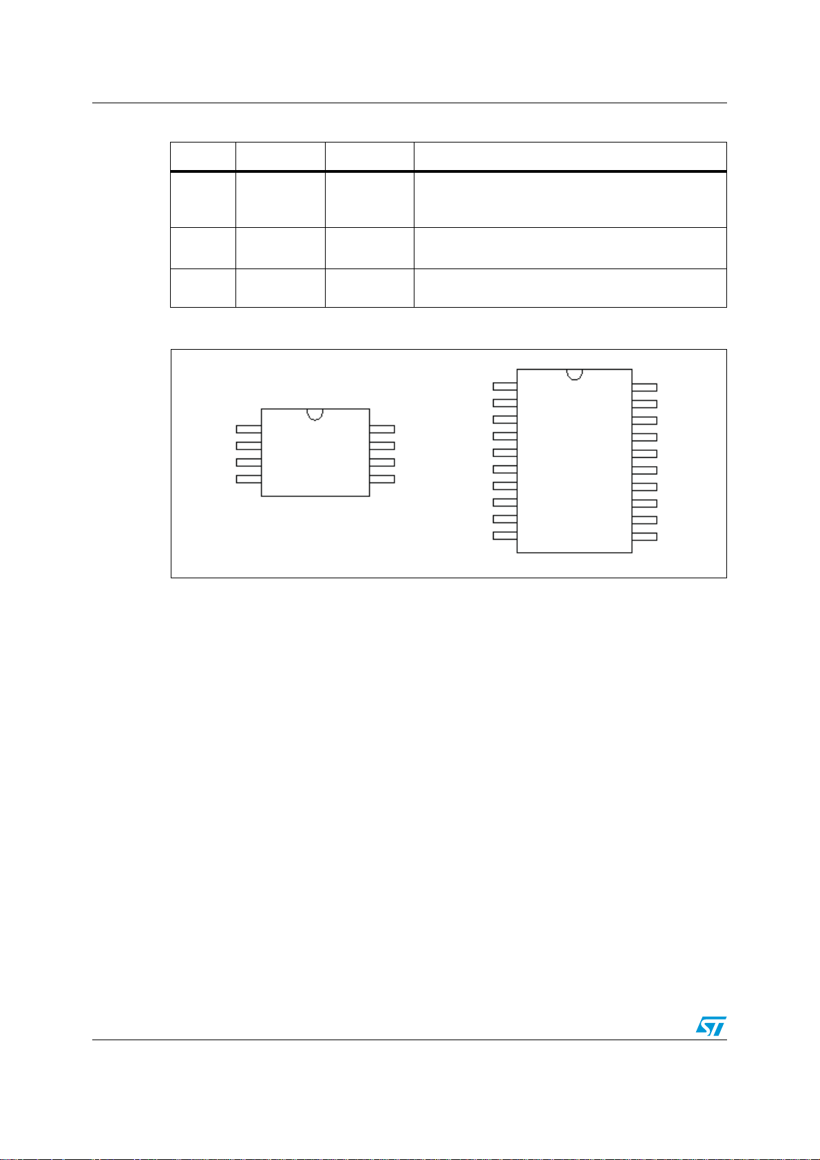
SO-8
SO-20
■ Operating DC supply voltage range 5.6 V to
31 V
■ Very low quiescent current with watchdog
disabled
■ Precision output voltage (3%)
■ Low drop voltage (180 mV typ at I
■ Reset circuit sensing the output voltage down
to 1 V
■ Programmable reset delay with external
capacitor
■ Watchdog disable input
■ Programmable watchdog timer with external
capacitor
■ Thermal shutdown and short circuit protection
■ Wide temperature range (T
= -40°C to 150°C)
j
= 150 mA)
o
L4989D
L4989MD
Low power voltage regulator
Datasheet − production data
Description
The L4989M and L4989MD are monolithic
integrated 5 V voltage regulators with a low drop
voltage at currents up to 150 mA.
The output voltage regulating element consists in
a p-channel MOS and the regulation is performed
regardless of input voltage transients up to 40 V.
The high precision of the output voltage is
obtained with a pre-trimmed reference voltage.
Table 1. Device summary
Package
SO-8 L4989D L4989D013TR
SO-20 L4989MD L4989MD013TR
The devices are protected against short circuit
and an overtemperature protection switches off
the devices in case of extremely high power
dissipation.
The L4989M and L4989MD watchdogs are active
when the Enable pin is high. Features like reset
and watchdog make this devices particularly
suitable to supply microprocessor systems in
automotive applications.
Order codes
Tube Tape and reel
April 2012 Doc ID 022376 Rev. 1 1/19
This is information on a product in full production.
www.st.com
1
Page 2

Contents L4989D, L4989MD
Contents
1 Block diagram and pin configuration . . . . . . . . . . . . . . . . . . . . . . . . . . 5
2 Electrical specifications . . . . . . . . . . . . . . . . . . . . . . . . . . . . . . . . . . . . . . 7
2.1 Absolute maximum ratings . . . . . . . . . . . . . . . . . . . . . . . . . . . . . . . . . . . . . 7
2.2 Thermal data . . . . . . . . . . . . . . . . . . . . . . . . . . . . . . . . . . . . . . . . . . . . . . . 7
2.3 Electrical characteristics . . . . . . . . . . . . . . . . . . . . . . . . . . . . . . . . . . . . . . . 8
3 Application information . . . . . . . . . . . . . . . . . . . . . . . . . . . . . . . . . . . . . 11
3.1 Voltage regulator . . . . . . . . . . . . . . . . . . . . . . . . . . . . . . . . . . . . . . . . . . . 11
3.2 Reset . . . . . . . . . . . . . . . . . . . . . . . . . . . . . . . . . . . . . . . . . . . . . . . . . . . . 11
3.3 Watchdog . . . . . . . . . . . . . . . . . . . . . . . . . . . . . . . . . . . . . . . . . . . . . . . . . 12
4 Package and packing information . . . . . . . . . . . . . . . . . . . . . . . . . . . . . 13
4.1 ECOPACK® packages . . . . . . . . . . . . . . . . . . . . . . . . . . . . . . . . . . . . . . . 13
4.2 SO-8 package information . . . . . . . . . . . . . . . . . . . . . . . . . . . . . . . . . . . . 13
4.3 SO-20 package information . . . . . . . . . . . . . . . . . . . . . . . . . . . . . . . . . . . 15
4.4 SO-8 packing information . . . . . . . . . . . . . . . . . . . . . . . . . . . . . . . . . . . . . 16
4.5 SO-20 packing information . . . . . . . . . . . . . . . . . . . . . . . . . . . . . . . . . . . . 17
5 Revision history . . . . . . . . . . . . . . . . . . . . . . . . . . . . . . . . . . . . . . . . . . . 18
2/19 Doc ID 022376 Rev. 1
Page 3

L4989D, L4989MD List of tables
List of tables
Table 1. Device summary . . . . . . . . . . . . . . . . . . . . . . . . . . . . . . . . . . . . . . . . . . . . . . . . . . . . . . . . . . 1
Table 2. Pins description . . . . . . . . . . . . . . . . . . . . . . . . . . . . . . . . . . . . . . . . . . . . . . . . . . . . . . . . . . 5
Table 3. Absolute maximum ratings . . . . . . . . . . . . . . . . . . . . . . . . . . . . . . . . . . . . . . . . . . . . . . . . . . 7
Table 4. Thermal data. . . . . . . . . . . . . . . . . . . . . . . . . . . . . . . . . . . . . . . . . . . . . . . . . . . . . . . . . . . . . 7
Table 5. General . . . . . . . . . . . . . . . . . . . . . . . . . . . . . . . . . . . . . . . . . . . . . . . . . . . . . . . . . . . . . . . . . 8
Table 6. Reset . . . . . . . . . . . . . . . . . . . . . . . . . . . . . . . . . . . . . . . . . . . . . . . . . . . . . . . . . . . . . . . . . . 9
Table 7. Watchdog . . . . . . . . . . . . . . . . . . . . . . . . . . . . . . . . . . . . . . . . . . . . . . . . . . . . . . . . . . . . . . . 9
Table 8. Watchdog Enable . . . . . . . . . . . . . . . . . . . . . . . . . . . . . . . . . . . . . . . . . . . . . . . . . . . . . . . . 10
Table 9. SO-8 mechanical data . . . . . . . . . . . . . . . . . . . . . . . . . . . . . . . . . . . . . . . . . . . . . . . . . . . . 14
Table 10. SO-20 mechanical data . . . . . . . . . . . . . . . . . . . . . . . . . . . . . . . . . . . . . . . . . . . . . . . . . . . 15
Table 11. Document revision history . . . . . . . . . . . . . . . . . . . . . . . . . . . . . . . . . . . . . . . . . . . . . . . . . 18
Doc ID 022376 Rev. 1 3/19
Page 4

List of figures L4989D, L4989MD
List of figures
Figure 1. Block diagram . . . . . . . . . . . . . . . . . . . . . . . . . . . . . . . . . . . . . . . . . . . . . . . . . . . . . . . . . . . . 5
Figure 2. Pins configuration (top view). . . . . . . . . . . . . . . . . . . . . . . . . . . . . . . . . . . . . . . . . . . . . . . . . 6
Figure 3. Behavior of output current versus regulated voltage V
Figure 4. Reset timing diagram . . . . . . . . . . . . . . . . . . . . . . . . . . . . . . . . . . . . . . . . . . . . . . . . . . . . . 12
Figure 5. Watchdog timing diagram . . . . . . . . . . . . . . . . . . . . . . . . . . . . . . . . . . . . . . . . . . . . . . . . . . 12
Figure 6. SO-8 package dimensions . . . . . . . . . . . . . . . . . . . . . . . . . . . . . . . . . . . . . . . . . . . . . . . . . 13
Figure 7. SO-20 package dimensions . . . . . . . . . . . . . . . . . . . . . . . . . . . . . . . . . . . . . . . . . . . . . . . . 15
Figure 8. SO-8 tube shipment (no suffix) . . . . . . . . . . . . . . . . . . . . . . . . . . . . . . . . . . . . . . . . . . . . . . 16
Figure 9. SO-8 tape and reel shipment (suffix “TR”) . . . . . . . . . . . . . . . . . . . . . . . . . . . . . . . . . . . . . 16
Figure 10. SO-20 tube shipment (no suffix) . . . . . . . . . . . . . . . . . . . . . . . . . . . . . . . . . . . . . . . . . . . . . 17
Figure 11. SO-20 tape and reel shipment (suffix “TR”) . . . . . . . . . . . . . . . . . . . . . . . . . . . . . . . . . . . . 17
. . . . . . . . . . . . . . . . . . . . . . . . . . . 11
o
4/19 Doc ID 022376 Rev. 1
Page 5

L4989D, L4989MD Block diagram and pin configuration
1 Block diagram and pin configuration
Figure 1. Block diagram
Table 2. Pins description
Pin name SO-8(D) S0-20(MD) Function
WE
n
11
Watchdog Enable input
If high watchdog functionality is active
Gnd 2 4 Ground reference
Gnd 5, 6, 15, 16
Ground.
Connected these pins to a heat spreader ground
Reset output.
Res 3 7
It is pulled down when output voltage goes below V
or frequency at Wi is too low.
Reset timing adjust.
Vcr 4 10
A capacitor between Vcr pin and gnd, sets the reset
delay time (t
)
rd
Watchdog timer adjust
Vcw 5 11
A capacitor between Vcw pin and gnd, sets the time
response of the watchdog monitor.
Watchdog input.
Wi 6 14
If the frequency at this input pin is too low, the Reset
output is activated.
o_th
Doc ID 022376 Rev. 1 5/10
Page 6
Block diagram and pin configuration L4989D, L4989MD
Table 2. Pins description (continued)
Pin name SO-8(D) S0-20(MD) Function
Voltage regulator output
V
o
717
Block to ground with a capacitor >100nF (needed for
regulator stability)
V
S
N.C.
820
2, 3, 8, 9, 12,
13, 18, 19
Supply voltage
Block to ground directly at IC pin with a capacitor
Not connected
Figure 2. Pins configuration (top view)
WEn
GND
Res
Vcr
1
2
SO-8
3
4
8
7
6
5
Vs
Vo
Wi
Vcw
WEn
N.C.
N.C.
GND
GND
GND
Res
N.C.
N.C.
Vcr
1
2
3
4
5
6
7
8
9
10
SO-20
20
19
18
17
16
15
14
13
12
11
GAPGCFT00666
Vs
N.C.
N.C.
Vo
GND
GND
Wi
N.C.
N.C.
Vcw
6/10 Doc ID 022376 Rev. 1
Page 7

L4989D, L4989MD Electrical specifications
2 Electrical specifications
2.1 Absolute maximum ratings
Table 3. Absolute maximum ratings
Symbol Parameter Value Unit
V
I
V
V
V
Vsdc
Vsdc
V
Vo
I
Vo
V
Wi
V
od
I
od
V
cr
cw
WEn
T
ESD
j
DC supply voltage -0.3 to 40 V
Input current Internally limited
DC output voltage -0.3 to 6 V
DC output current Internally limited
Watchdog input voltage -0.3 to VVo + 0.3 V
Open Drain output voltage -0.3 to VVo + 0.3 V
Open Drain output current Internally limited
Reset delay voltage -0.3 to VVo + 0.3 V
Watchdog delay voltage -0.3 to VVo + 0.3 V
Watchdog Enable input voltage -0.3 to 40 V
Junction temperature -40 to 150 “C
ESD voltage level (HBM-MIL STD 883C) ±2 kV
Note: Maximum ratings are absolute ratings; exceeding any one of these values may cause
permanent damage to the integrated circuit.
2.2 Thermal data
Table 4. Thermal data
Symbol Parameter S0-8 S0-12+4+4 Unit
R
th-jamb
1. With 6 sq. cm on board heat sink.
Thermal resistance junction to ambient 130 to 180 50
(1)
Doc ID 022376 Rev. 1 7/10
°C/W
Page 8

Electrical specifications L4989D, L4989MD
2.3 Electrical characteristics
VS = 5.6 V to 31 V, Tj= -40°C to +150°C unless otherwise specified.
Table 5. General
Pin Symbol Parameter Test condition Min. Typ. Max. Unit
V
o
V
o
V
o
V
, V
S
V
o
VS, V
V
, V
S
, V
V
S
V
, V
S
V
, V
S
V
, V
S
V
, V
S
V
, V
S
V
, V
S
V
, V
S
V
o_ref
I
short_13
I
lim
V
o
o
o
line
V
load
V
dp
SVR Ripple rejection fr = 100 Hz 55 dB
Output voltage
Short circuit current VS= 13.5 V
Output current limitation VS= 13.5 V
Line regulation voltage
Load regulation voltage Io= 1 to 150 mA 25 mV
Drop voltage Io= 150 mA 180 400 mV
Current consumption with
I
o
qs_1
watchdog not active
I
qs_1=IVS-Io
Current consumption with
I
o
qs_10
watchdog not active
I
qs_10=IVS-Io
Current consumption with
I
o
qs_50
watchdog not active
I
qs_50=IVS-Io
Current consumption with
I
o
qs_150
watchdog not active
I
qs_150=IVS-Io
Current consumption with
I
o
qn_1
watchdog active
I
qn_1=IVS-Io
Current consumption with
I
o
qn_10
watchdog active
I
qn_10=IVS-Io
Current consumption with
I
o
qn_50
watchdog active
I
qn_50=IVS-Io
Current consumption with
I
o
qn_150
Tw
watchdog active
I
qn_150=IVS-Io
Thermal protection
temperature
VS= 5.6 to 31 V;
I
= 1 to 150 mA
o
(1)
(1)
= 5.6 to 31 V;
V
S
= 1 to 150 mA
I
o
VS= 13.5 V;
I
<1mA;
o
=low
WE
n
VS= 13.5 V;
I
=10mA;
o
=low
WE
n
VS= 13.5 V;
I
=50mA;
o
=low
WE
n
VS= 13.5 V;
I
=150mA;
o
=low
WE
n
VS= 13.5 V;
I
<1mA;
o
=high
WE
n
VS= 13.5 V;
I
=10mA;
o
=high
WE
n
VS= 13.5 V;
I
=50mA;
o
=high
WE
n
VS= 13.5 V;
I
=150mA;
o
=high
WE
n
4.85 5.0 5.15 V
160 210 250 mA
170 250 290 mA
69 115 µA
127 300 µA
498 900 µA
1.40 2 mA
110 170 µA
168 350 µA
538 1000 µA
1.45 2 mA
150 190 °C
25 mV
Tw _hy
1. See Figure 3.
Thermal protection
temperature hysteresis
8/10 Doc ID 022376 Rev. 1
10 °C
Page 9

L4989D, L4989MD Electrical specifications
T able 6. Reset
Pin Symbol Parameter Test condition Min. Typ. Max. Unit
R
=5kΩ to Vo;
Res Vres_l Reset output low voltage
Res I
Res R
Res V
Vcr V
Vcr V
Vcr I
Vcr I
Res T
Res T
1. When Vo becomes lower than 4V, the reset reaction time decreases down to 2µs assuring a faster reset
condition in this particular case.
Res_lkg
Res
o_th
rlth
rhth
cr
dr
rr_2
rd
Reset output high leakage
current
Pull up internal resistance Versus V
Reset threshold voltage
Reset timing low threshold VS= 13.5 V 10% 13% 16%
Reset timing high threshold VS= 13.5 V 44% 47% 50%
Charge current VS= 13.5 V 8 15 30 µA
Discharge current VS= 13.5 V 8 15 30 µA
Reset reaction time
(1)
Reset delay time
ext
V
>1V
o
=5V 1 µA
V
Res
o
= 5.6 to 31 V;
V
S
= 1 to 150 mA
I
o
Vo=V
o_th
= 13.5 V;
V
S
Ctr = 1 nF
-100 mV 100 250 700 µs
10 20 50 kΩ
6% 8% 10%
65 115 165 ms
0.4 V
Below
V
o_ref
V
o_ref
V
o_ref
Table 7. Watchdog
Pin Symbol Parameter Test condition Min. Typ. Max. Unit
Wi Vih Input high voltage V
Wi Vil Input low voltage V
Wi Vih Input hysteresis V
= 13.5 V 3.5 V
S
= 13.5 V 1.5 V
S
= 13.5 V 500 mV
S
Wi Rwi Pull down resistor VS= 13.5 V 30 100 250 KΩ
Vcw Vwhth High threshold V
= 13.5 V 44% 47% 50%
S
Vcw Vwlth Low threshold VS= 13.5 V 10% 13% 16%
= 13.5 V;
V
Vcw Icwc Charge current
Vcw Icwd Discharge current
Vcw Twop Watchdog period
Res twol Watchdog output low time
S
Vcw = 0.1 V
= 13.5 V;
V
S
Vcw = 2.5 V
= 13.5 V;
V
S
Ctw = 47 nF
= 13.5 V;
V
S
Ctw = 47 nF
51020µA
1.25 2.5 5 µA
20 40 80 ms
4816ms
V
V
o_ref
o_ref
Doc ID 022376 Rev. 1 9/10
Page 10

Electrical specifications L4989D, L4989MD
Table 8. Watchdog Enable
Pin Symbol Parameter Test condition Min. Typ. Max. Unit
WE
WE
WE
WE
V
n
n
n
n
WEn_l
V
WEn_h
V
WEn_hy
I_leak Pull down current VS= 13.5 V 1 2.5 5 µA
Enable input low voltage 1 V
Enable input high voltage 3 V
Enable input hysteresis 600 920 1300 mV
10/10 Doc ID 022376 Rev. 1
Page 11

L4989D, L4989MD Application information
Vo
Vo_ref
IoutIshort Ilim
3 Application information
3.1 Voltage regulator
The voltage regulator uses a p-channel MOS transistor as a regulating element. With this
structure a very low dropout voltage at current up to 150 mA is obtained. The output voltage
is regulated up to transient input supply voltage of 40 V. No functional interruption due to
over-voltage pulses is generated.The voltage Regulator is always active and not depending
on the state of WE
input pin. A short circuit protection to GND is provided.
n
Figure 3. Behavior of output current versus regulated voltage V
3.2 Reset
The reset circuit supervises the output voltage Vo. The V
the in-ternal reference voltage and a resistor output divider. If the output voltage becomes
lower than V
guaranteed for an output voltage V
When the output voltage becomes higher than V
This delay is obtained by an internal oscillator.
The oscillator period is given by:
T
osc
where:
I
cr
I
dr
V
rhth
C
tr
t
is given by:
rd
t
rd
The Reset is always active and not depending on the state of WEn input pin.
reset threshold is defined with
o_th
then Res goes low with a reaction time trr. The reset low signal is
o_th
= [(V
rhth-Vrlth
) x Ctr] / Icr + [(V
greater than 1 V.
o
o_th
rhth-Vrlth
) x Ctr] / I
then Res goes high with a delay trd.
dr
: is an internally generated charge current
: is an internally generated discharge current
, V
: are two voltages defined with the output voltage and a resistor output
rlth
divider
: is an external capacitance.
= 512 x T
osc
o
Doc ID 022376 Rev. 1 11/10
Page 12

Application information L4989D, L4989MD
TRR
TRR
TRD4 OSC
4OSC
6RHTH
6RLTH
2ES
6CR
6O
7I
6OUT?TH
'!0'#&4
7I
6CW
2ES
6WLTH
6WHTH
TWOP
TWOL
6WLTH
("1($'5
Figure 4. Reset timing diagram
3.3 Watchdog
A connected microcontroller is monitored by the watchdog input Wi. If pulses are missing,
the Reset output pin is set to low. The pulse sequence time can be set within a wide range
with the external capacitor, C
constant current I
. If the lower threshold V
cwd
To prevent this the microcontroller must generate a positive edge during the discharge of the
capacitor before the voltage has reached the threshold V
minimum time t, during which the micro-controller must output the positive edge, the
following equation can be used:
Every Wi positive edge switches the current source from discharging to charging. The same
happens when the lower threshold is reached. When the voltage reaches the upper
threshold, V
, the current switches from charging to discharging. The result is a saw-tooth
whth
voltage at the watchdog timer capacitor C
. The watchdog circuit discharges the capacitor Ctw, with the
tw
(V
whth-Vwlth
is reached, a watchdog reset is generated.
wlth
. In order to calculate the
wlth
tw
.
) x Ctw = I
cwd
x t
Figure 5. Watchdog timing diagram
12/10 Doc ID 022376 Rev. 1
Page 13

L4989D, L4989MD Package and packing information
'!0'#&4
4 Package and packing information
4.1 ECOPACK® packages
In order to meet environmental requirements, ST offers these devices in different grades of
ECOPACK
®
packages, depending on their level of environmental compliance. ECOPACK®
specifications, grade definitions and product status are available at: www.st.com.
ECOPACK
®
is an ST trademark.
4.2 SO-8 package information
Figure 6. SO-8 package dimensions
Doc ID 022376 Rev. 1 13/10
Page 14

Package and packing information L4989D, L4989MD
T able 9. SO-8 mechanical data
Symbol
Min. Typ. Max.
A 1.75
A1 0.10 0.25
A2 1.25
b0.28 0.48
c0.17 0.23
(1)
D
4.80 4.90 5.00
E 5.80 6.00 6.20
(2)
E1
3.80 3.90 4.00
e1.27
h0.25 0.50
L0.40 1.27
Millimeters
L1 1.04
k0° 8°
ccc 0.10
1. Dimensions D does not include mold flash, protrusions or gate burrs. Mold flash, potrusions or gate burrs
shall not exceed 0.15mm in total (both side).
2. Dimension “E1” does not include interlead flash or protrusions. Interlead flash or protrusions shall not
exceed 0.25mm per side.
14/10 Doc ID 022376 Rev. 1
Page 15

L4989D, L4989MD Package and packing information
4.3 SO-20 package information
Figure 7. SO-20 package dimensions
T able 10. SO-20 mechanical data
Symbol
Min. Typ. Max.
A2.35 2.65
A1 0.10 0.30
B0.33 0.51
C0.23 0.32
(1)
D
12.60 13.00
E7.40 7.60
e1.27
H 10.0 10.65
h0.25 0.75
L0.40 1.27
k0° 8°
ddd 0.10
Millimeters
1. “D” dimension does not include mold flash, protusions or gate burrs. Mold flash, protusions or gate burrs
shall not exceed 0.15mm per side.
Doc ID 022376 Rev. 1 15/10
Page 16

Package and packing information L4989D, L4989MD
All dimensions are in mm.
Base Q.ty 100
Bulk Q.ty 2000
Tube length (± 0.5) 532
A 3.2
B 6
C (± 0.1) 0.6
C
B
A
Tape dimensions
According to Electronic Industries Association
(EIA) Standard 481 rev. A, Feb. 1986
All dimensions are in mm.
Tape width W 12
Tape Hole Spacing P0 (± 0.1) 4
Component Sp acing P 8
Hole Diameter D (+0.1/-0) 1.5
Hole Diameter D1 (min) 1.5
Hole Position F (± 0.05) 5.5
Compartment Depth K (max) 4.5
Hole Spacing P1 (± 0.1) 2
Top
cover
tape
End
Start
No componentsNo components Components
500mm min
500mm min
Empty components pockets
saled with cover tape.
User direction of feed
Reel dimensions
All dimensions are in mm.
Base Q.ty 2500
Bulk Q.ty 2500
A (max) 330
B (min) 1.5
C (± 0.2) 13
F 20.2
G (+ 2 / -0) 12.4
N (min) 60
T (max) 18.4
4.4 SO-8 packing information
Figure 8. SO-8 tube shipment (no suffix)
Figure 9. SO-8 tape and reel shipment (suffix “TR”)
16/10 Doc ID 022376 Rev. 1
Page 17

L4989D, L4989MD Package and packing information
All dimensions are in mm.
Base Q.ty 40
Bulk Q.ty 800
Tube length (± 0.5) 532
A 3.5
B 13.8
C (± 0.1) 0.6
A
C
B
Base Q.ty 1000
Bulk Q.ty 1000
A (max) 330
B (min) 1.5
C (± 0.2) 13
D 20.2
G (+ 2 / -0) 24.4
N (min) 60
T (max) 30.4
Tape dimensions
According to Electronic Industries Association
(EIA) Standard 481 rev. A, Feb. 1986
All dimensions are in mm.
Tape width W 24
Tape Hole Spacing P0 (± 0.1) 4
Component Spacing P 12
Hole Diameter D (+0.1/-0) 1.5
Hole Diameter D1 (min) 1.5
Hole Position F (± 0.05) 11.5
Compartment Depth K (max) 6.5
Hole Spacing P1 (± 0.1) 2
Top
cover
tape
End
Start
No componentsNo components Components
500mm min
500mm min
Empty components pockets
saled with cover tape.
User direction of feed
Reel dimensions
4.5 SO-20 packing information
Figure 10. SO-20 tube shipment (no suffix)
Figure 11. SO-20 tape and reel shipment (suffix “TR”)
Doc ID 022376 Rev. 1 17/10
Page 18

Revision history L4989D, L4989MD
5 Revision history
Table 11. Document revision history
Date Revision Changes
16-Apr-2012 1
Initial release.
This document replace the L4989 datasheet.
18/10 Doc ID 022376 Rev. 1
Page 19

L4989D, L4989MD
Please Read Carefully:
Information in this document is provided solely in connection with ST products. STMicroelectronics NV and its subsidiaries (“ST”) reserve the
right to make changes, corrections, modifications or improvements, to this document, and the products and services described herein at any
time, without notice.
All ST products are sold pursuant to ST’s terms and conditions of sale.
Purchasers are solely responsible for the choice, selection and use of the ST products and services described herein, and ST assumes no
liability whatsoever relating to the choice, selection or use of the ST products and services described herein.
No license, express or implied, by estoppel or otherwise, to any intellectual property rights is granted under this document. If any part of this
document refers to any third party products or services it shall not be deemed a license grant by ST for the use of such third party products
or services, or any intellectual property contained therein or considered as a warranty covering the use in any manner whatsoever of such
third party products or services or any intellectual property contained therein.
UNLESS OTHERWISE SET FORTH IN ST’S TERMS AND CONDITIONS OF SALE ST DISCLAIMS ANY EXPRESS OR IMPLIED
WARRANTY WITH RESPECT TO THE USE AND/OR SALE OF ST PRODUCTS INCLUDING WITHOUT LIMITATION IMPLIED
WARRANTIES OF MERCHANTABILITY, FITNESS FOR A PARTICULAR PURPOSE (AND THEIR EQUIVALENTS UNDER THE LAWS
OF ANY JURISDICTION), OR INFRINGEMENT OF ANY PATENT, COPYRIGHT OR OTHER INTELLECTUAL PROPERTY RIGHT.
UNLESS EXPRESSLY APPROVED IN WRITING BY TWO AUTHORIZED ST REPRESENTATIVES, ST PRODUCTS ARE NOT
RECOMMENDED, AUTHORIZED OR WARRANTED FOR USE IN MILITARY, AIR CRAFT, SPACE, LIFE SAVING, OR LIFE SUSTAINING
APPLICATIONS, NOR IN PRODUCTS OR SYSTEMS WHERE FAI LURE OR MALFUNCTION MAY RESULT IN PERS ONAL INJURY,
DEATH, OR SEVERE PROPERTY OR ENVIRONMENTAL DAMAGE. ST PRODUCTS WHICH ARE NOT SPECIFIED AS "AUTOMOTIVE
GRADE" MAY ONLY BE USED IN AUTOMOTIVE APPLICATIONS AT USER’S OWN RISK.
Resale of ST products with provisions different from the statements and/or technical features set forth in this document shall immediately void
any warranty granted by ST for the ST product or service described herein and shall not create or extend in any manner whatsoever, any
liability of ST.
ST and the ST logo are trademarks or registered trademarks of ST in various countries.
Information in this document supersedes and replaces all information previously supplied.
The ST logo is a registered trademark of STMicroelectronics. All other names are the property of their respective owners.
© 2012 STMicroelectronics - All rights reserved
STMicroelectronics group of companies
Australia - Belgium - Brazil - Canada - China - Czech Republic - Finland - France - Germany - Hong Kong - India - Israel - Italy - Japan -
Malaysia - Malta - Morocco - Philippines - Singapore - Spain - Sweden - Switzerland - United Kingdom - United States of America
www.st.com
Doc ID 022376 Rev. 1 19/19
 Loading...