

L4981A
®
CONTROL BOOST PWM UP TO 0.99P.F.
LIMIT LINE CURRENT DISTORTION TO < 5%
UNIVERSAL INPUT MAINS
FEED FORWARD LINE AND LOAD REGULA-
TION
AVERAGE CURRENT MODE PWM FOR
MINIMUM NOISE SENSITIVITY
HIGH CURRENT BIPOLAR AND DMOS TO-
TEM POLE OUTPUT
LOW START-UP CURRENT (0.3mA TYP.)
UNDER VOLTAGE LOCKOUT WITH HYS-
TERESIS AND PROGRAMMABLE TURN ON
THRESHOLD
OVERVOLTAGE, OVERCURRENT PROTECTION
PRECISE 2% ON CHIP REFERENCE EXTERNALLY AVAILABLE
SOFT START
DESCRIPTION
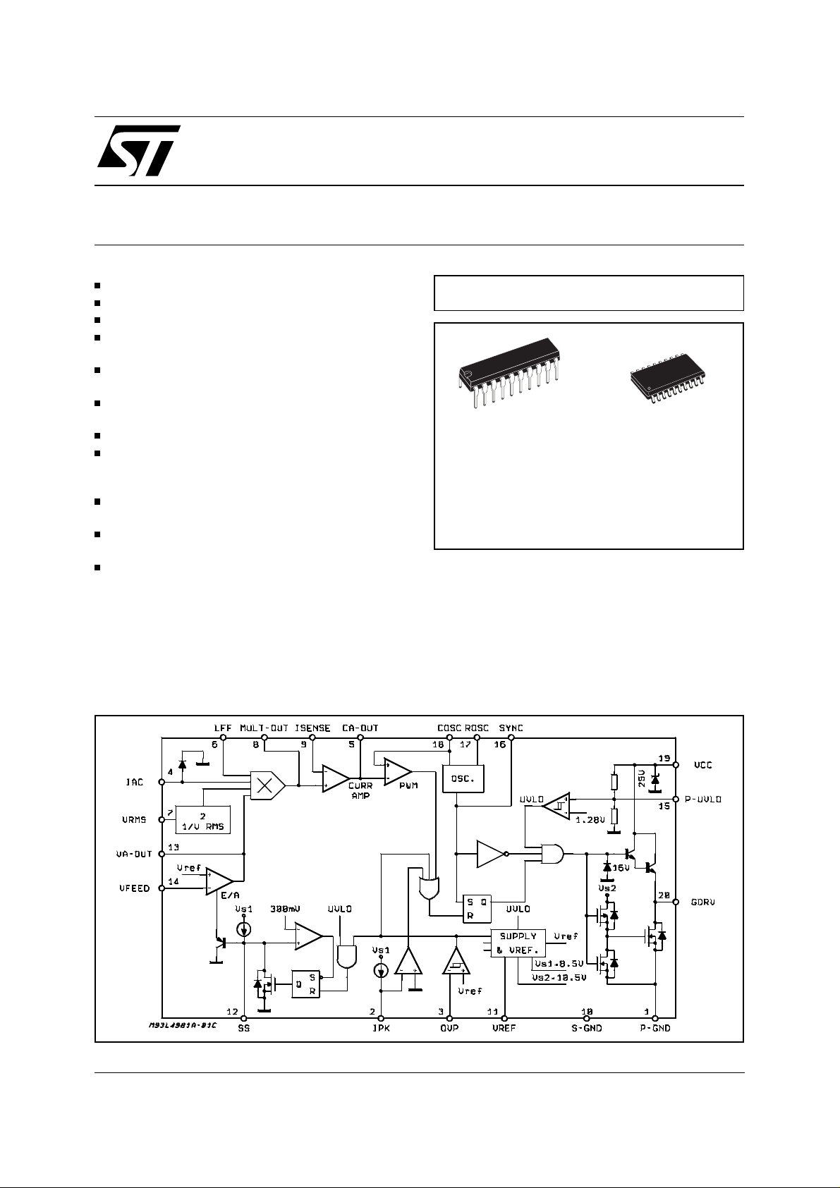
The L4981 I.C. provides the necessary features
to achieve a very high power factor up to 0.99.
Realized in BCD 60II technology this power factor
corrector (PFC) pre-regulator contains all the con-
L4981B
POWER FACT O R CORR ECTOR
MULTIPOWER BCD TECHNOLOGY
DIP20 SO20
ORDERING NUMBERS:
L4981XD (SO20)
trol functions for designing a high efficiency-mode
power supply with sinusoidal line current consumption.
The L4981 can be easily used in systems with
mains voltages between 85V to 265V without any
line switch. This new PFC offers the possibility to
work at fixed frequency (L4981A) or modulated
frequency (L4981B) optimizing the size of the in-
L4981X (DIP20)
BLOCK DIAGRAM
November 2001
1/16
L4981A - L4981B
put filter; both the operating frequency modes
working with an average current mode PWM controller, maintaining sinusoidal line c urrent without
slope compensation.
Besides power MOSFET gate driver, precise voltage reference (externally available), error ampli-
soft start are included. To limit the number of the
external components, the device integrates protections as overvoltage and overcurrent. The
overcurrent level can be programmed using a
simple resistor for L4981A. For a better precision
and for L4981B an external divider must be used.
fier, undervoltage lockout, current sense and the
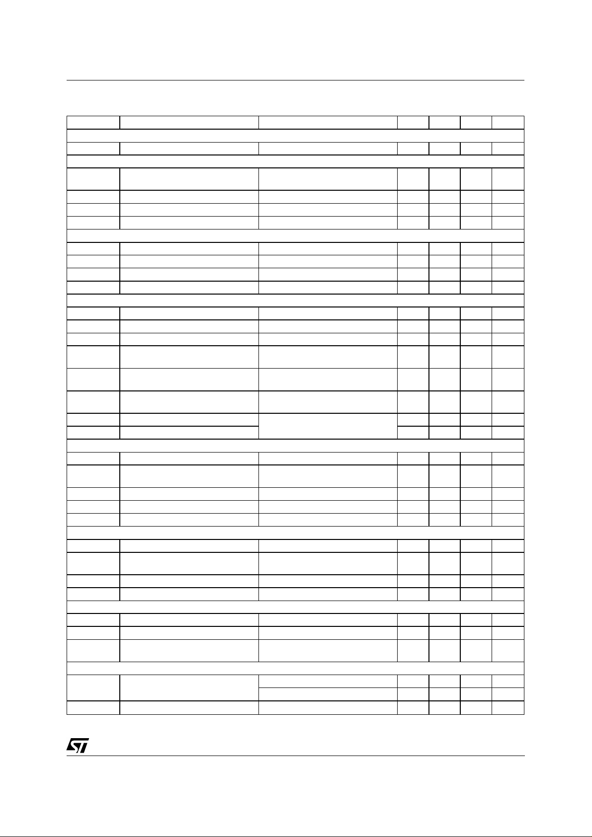
ABSOLUTE MAXIMUM RATINGS
Symbol Pin Parameter Value Unit
V
CC
I
GDRV
V
GDRV
V
VA-OUT
I
AC
V
CA-OUT
V
ROSC
I
COSC
I
FREQ-MOD
V
SYNC
V
IPK
P
tot
T
op
T
stg
(*) Maximum package power dissipation limits must be observed.
19 Supply Voltage (ICC ≤50mA) (*) selflimit V
20 Gate driv. output peak current (t = 1µs) SINK 2 Α
. SOURCE 1.5 A
Gate driv. output voltage t = 0.1µs-1V
Voltages at pins 3, 14, 7, 6, 12, 15 -0.3 to 9 V
13 Error Amplifier Voltage -0.3 to 8.5 V
4 AC Input Current 5 mA
Voltages at pin 8, 9 -0.5 to 7 V
5 Current Amplifier Volt. (Isource = -20mA; Isink = 20mA) -0.3 to 8.5 V
17 Voltage at pin 17 -0.3 to 3 V
11, 18 Voltage at pin 11, 18 -0.3 to 7 V
18 Input Sink Current 15 mA
16 Frequency Modulation Sink Current (L4981B) 5 mA
16 Sync. Voltage (L4981A) -0.3 to 7 V
2 Voltage at pin 2
Voltage at Pin 2 t = 1µs
Power Dissipation at T
Power Dissipation at T
= 70°C (DIP20) 1 W
amb
= 70°C (SO20) 0.6 W
amb
-0.3 to 5.5
-2
Operating Ambient Temperature -40 to 125 °C
StorageTemperature -55 to 150 °C
V
V
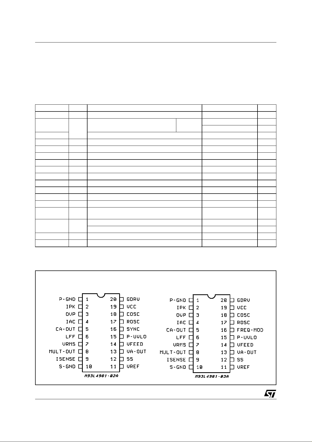
PIN CONNECTIONS
2/16
(Top views)
L4981A
L4981B
L4981A - L4981B
THERMAL DATA
Symbol Parameter DIP 20 SO 20 Unit
R
th j-amb
PIN FUNCTIONS
N. Name Description
1 P-GND Power ground.
2 IPK
Thermal Resistance Junction-ambient 80 120 °C/W
L4981A
peak current limiting. A current limitation is obtained using a single resistor connected
between Pin 2 and the sense resistor. To have a better precision another resistor between Pin
2 and a reference voltage (Pin 11) must be added.
L4981B
peak current limiting. A precise current limitation is obtained using two external
resistor only. These resistors must be connected between the sense resistor, Pin 2 and the
reference voltage.
3 OVP Overvoltage protection. At this input are compared an internal precise 5.1V (typ) voltage
reference with a sample of the boost output voltage obtained via a resistive voltage divider in
order to limit the maximum output peak voltage.
4 IAC Input for the AC current. An input current proportional to the rectified mains voltage generates,
via a multiplier, the current reference for the current amplifier.
5 CA-OUT Current amplifier output. An external RC network determinates the loop gain.
6 LFF Load feedforward; this voltage input pin allows to modify the multiplier output current
proportionally to the load, in order to give a faster response versus load transient. The best
control is obtained working between 1.5V and 5.3V. If this function is not used, connect this pin
to the voltage reference (pin = 11).
7 VRMS Input for proportional RMS line voltage. the VRMS input compesates the line voltage changes.
Connecting a low pass filter between the rectified line and the pin 7, a DC voltage proportional
to the input line RMS voltage is obtained. The best control is reached using input voltage
between 1.5V and 5.5V. If this function is not used connect this pin to the voltage reference
(pin = 11).
8 MULT-OUT Multiplier output. This pin common to the multiplier output and the current amplifier N.I. input is
. The MULT-OUT pin must be taken not below -0.5V.
SENSE
9I
SENSE
an high impedence input like I
Current amplifier inverting input. Care must be taken to avoid this pin goes down -0.5V.
10 S-GND Signal ground.
11 V
REF
Output reference voltage (typ = 5.1V).Voltage refence at ± 2% of accuracy externally available,
it’s internally current limited and can deliver an output current up to 10mA.
12 SS A capacitor connected to ground defines the soft start time. An internal current generator
delivering 100µA (typ) charges the external capacitor defining the soft start time constant. An
internal MOS discharge, the external soft start capacitor both in overvoltage and UVLO
conditions.
13 VA-OUT Error amplifier output, an RC network fixes the voltage loop gain characteristics.
14 VFEED Voltage error amplifier inverting input. This feedback input is connected via a voltage divider to
the boost output voltage.
15 P-UVLO Programmable under voltage lock out threshold input. A voltage divider between supply
voltage and GND can be connected in order to program the turn on threshold.
16 SYNC
(L4981A)
This synchronization input/output pin is CMOS logic compatible. Operating as SYNC in, a
rectangular wave must be applied at this pin. Opearting as SYNC out, a rectangular clock
pulse train is available to synchronize other devices.
FREQ-MOD
(L4981B)
17 R
18 C
19 V
OSC
OSC
CC
Frequency modulation current input. An external resistor must be connected between pin 16
and the rectified line voltage in order to modulate the oscillator frequency. Connecting pin 16 to
ground a fixed frequency imposed by R
OSC
and C
An external resistor connected to ground fixes the constant charging current of C
is obtained.
OSC
OSC
.
An external capacitor connected to GND fixes the switching frequency.
Supply input voltage.
20 GDRV Output gate driver. Bipolar and DMOS transistors totem pole output stage can deliver peak
current in excess 1A useful to drive MOSFET or IGBT power stages.
3/16
L4981A - L4981B
ELECTRICAL CHARACTERISTICS
= 24KΩ, CSS = 1µF, V
R
OSC
= GND, V
V
FEED
= 1V, V
IPK
OVP
= 3.5V, V
CA-OUT
= 1V, TJ = 25°C
(Unless otherwise specified V
ISENSE
= 0V, V
LFF
= V
= 18V, C
CC
, IAC = 100µA, V
REF
OSC
= 1nF,
RMS
= 1V,
Symbol Prameter Test Condition Min. Typ. Max. Unit
ERROR AMPLIFIER SECTION
V
IO
IIBInput Bias Current V
Input Offset Voltage –25°C < TJ < 85°C ±8mV
= 0V -500 -50 500 nA
FEED
Open Loop Gain 70 100 dB
V
13H
V
13L
-I
13
I
13
Output High voltage V
Output Low Voltage V
Output Source Current V
Output Sink Current V
FEED
I
VA-OUT
FEED
I
VA-OUT
FEED
FEED
= 4.7V
= -0.5mA
= 5.5V
= 0.5mA
= 4.7V; V
= 5.5V; V
5.5 6.5 7.5 V
0.4 1 V
= 3.5V 2 10 mA
VA-OUT
= 3.5V 4 20 mA
VA-OUT
REFERENCE SECTION
V
ref
∆V
∆V
I
ref sc
Reference Output Voltage –25°C < TJ < 85°C 4.97 5.1 5.23 V
T
Load Regulation 1mA ≤ I
ref
–25°C < T
Line Regulation 12V ≤ VCC ≤ 19V
ref
–25°C < T
Short Circuit Current V
= 25°C I
j
= 0V 20 30 50 mA
ref
= 0 5.01 5.1 5.19 V
ref
≤ 10mA
ref
< 85°C
J
315mV
310mV
< 85°C
J
OSCILLATOR SECTION
f
osc
V
svp
I
18C
I
18D
V
18
SYNC SECTION
t
W
I
16
-I
16
V
16L
V
16H
t
d
FREQUENCY MODULATION FUNCTION
f
18max
f
18min
Initial Accuracy Tj = 25°C 85 100 115 KHz
Frequency Stability 12V ≤ VCC ≤ 19V
–25°C < T
< 85°C
J
80 100 120 KHz
Ramp Valley to Peak 4.7 5 5.3 V
Charge Current V
Discharge Current V
= 3.5V 0.45 0.55 0.65 mA
COSC
= 3.5V 11.5 mA
COSC
Ramp Valley Voltage 0.9 1.15 1.4 V
(Only for
L4981A
)
Output Pulse Width 50% Amplitude 0.3 0.8 µs
Sink Current with Low Output
Voltage
Source Current with High Output
Voltage
V
V
V
V
SYNC
COSC
SYNC
COSC
= 0.4V
= 0V
= 4.5V
= 6.7V
0.4 0.8 mA
16 mA
Low Input Voltage 0.9 V
High Input Voltage 3.5 V
Pulse for Synchronization 800 ns
(Only for
Maximum Oscillation Frequency V
Minimum Oscillator Frequency I
L4981B
FREQ-MOD
FREQ-MOD
V
= 4V (Pin 7)
VRMS
I
FREQ-MOD
V
= 2V (Pin 7)
VRMS
)
= 0V (Pin 16) I
= 360µA (Pin 16)
= 180µA (Pin 16)
= 0 85 100 115 KHz
freq
74 KHz
76 KHz
SOFT START SECTION
V
I
SS
12sat
Soft Start Source Current VSS = 3V 60 100 140 µA
Output Saturation Voltage V3 = 6V, ISS = 2mA 0.1 0.25 V
4/16
L4981A - L4981B
ELECTRICAL CHARACTERISTICS
(continued)
Symbol Parameter Test Condition Min. Typ. Max. Unit
SUPPLY VOLTAGE
V
CC
Operating Supply Voltage 19.5 V
OVER VOLTAGE PROTECTION COMPARATOR
V
thr
V
3Hys
I
3
t
d
Rising Threshold Voltage V
-20mV
ref
5.1 V
+20mV
ref
Hysteresis 180 250 320 mV
Input Bias Current 0.05 1 µA
Propagation delay to output V
OVP
= V
+100mV 1 2 µs
thr
OVER CURRENT PROTECTION COMPARATOR
V
th
t
d
I
ipk
I
L
Threshold Voltage ±30 mV
Propagation delay to Output V
Current Source Generator V
Leakage Current V
= V
OCP
= -0.1V
IPK
= -0.1V
IPK
-0.2V 0.4 0.9 µs
thr
only for L4981A
only for L4981B
65 85 105 µA
5 µA
CURRENT AMPLIFIER SECTION
V
offset
I
9bias
SVR Supply Voltage Rejection 12V ≤ V
V
5H
V
5L
-I
5
I
5
Input Offset Voltage V
Input Bias Current V
MULT OUT
SENSE
Open Loop Gain 1.1V ≤ V
V
MULT OUT
Output High Voltage V
Output Low Voltage V
Output Source Current V
Output Sink Current 2 10 mA
MULT OUT
I
CA OUT
MULT OUT
I
CA OUT
MULT OUT
V
IAC
= V
= 3.5V ±2mV
SENSE
= 0V -500 50 500 nA
≤ 6V 70 100 dB
CA OUT
≤ 19V
CC
= 3.5V V
= 200mV
= -0.5mA, V
= -200mV
= 0.5mA, V
= 200mV,
= 0V, V
CA-OUT
SENSE
= 0V
IAC
= 0V
IAC
= 3.5V
= 3.5V
68 90 dB
6.2 V
0.9 V
210 mA
OUTPUT SECTION
V
V
V
GDRV
20L
20H
t
r
t
f
Output Voltage Low I
Output Voltage High I
Output Voltage Rise Time C
Output Voltage Fall Time C
Voltage Clamp I
= 250mA 0.5 0.8 V
SINK
= 250mA
SOURCE
V
= 15V
CC
= 1nF 50 150 ns
OUT
= 1nF 30 100 ns
OUT
= 0mA 13 16 19 V
SOURCE
11.5 12.5 V
TOTAL STANDBY CURRENT SECTION
I
19start
I
19on
Supply Current before start up VCC = 14V 0.3 0.5 mA
Supply Current after turn on V
= 0V, V
IAC
COSC
= 0,
812mA
Pin17 = Open
I
19
V
CC
Operating Supply Current Pin20 = 1nF 12 16 mA
Zener Voltage (*) 20 25 30 V
UNDER VOLTAGE LOCKOUT SECTION
V
V
th ON
th OFF
Turn on Threshold 14.5 15.5 16.5 V
Turn off Threshold 9 10 11 V
Programmable Turn-on Threshold Pin 15 to VCC = 220K
10.6 12 13.4 V
Pin15 to GND = 33K
LOAD FEED FORWARD
I
LFF
V
(*) Maximum package power dissipation limits must be observed.
Bias Current V6 = 1.6V 70 140 µA
= 5.3V 200 300 µA
V
6
Input Voltage Range 1.6 5.3 V
I
V
5/16

L4981A - L4981B
ELECTRICAL CHARACTERISTICS
(continued)
Symbol Prameter Test Condition Min. Typ. Max. Unit
MULTIPLIER SECTION
Multipler Output Current V
= 4V, V
VA-OUT
V
I
AC
V
V
I
AC
V
V
I
AC
V
V
I
AC
V
V
I
AC
V
V
C
V
V
I
AC
V
V
I
AC
= 0, V
MULTOUT
= 50µA, C
= 4V, V
VA-OUT
= 0, V
MULTOUT
= 200µA, C
= 2V, V
VA-OUT
= 0, V
MULTOUT
= 100µA, C
= 2V, V
VA-OUT
= 0, V
MULTOUT
= 100µA, C
= 4V, V
VA-OUT
= 0, V
MULTOUT
= 100µA, C
= 4V, V
VA-OUT
= 0, V
MULTOUT
= 0V, IAC = 200µA
OSC
= 4V, V
VA-OUT
= 0, V
MULTOUT
= 200µA, C
= 2V, V
VA-OUT
= 0, V
MULTOUT
= 0, C
OSC
RMS
LFF
OSC
RMS
LFF
OSC
RMS
LFF
OSC
RMS
LFF
OSC
RMS
LFF
OSC
RMS
LFF
RMS
LFF
OSC
RMS
LFF
= 0V
= 2V,
= 5.1V
= 0V
= 2V,
= 5.1V
= 0V
= 2V,
= 5.1V
= 0V
= 4V,
= 5.1V
= 0V
= 4V,
= 5.1V
= 0V
= 2V,
= 2.5V
= 4V
= 5.1V
= 0V
= 4V,
= 5.1V
20 35 52 µA
100 135 170 µA
10 20 30 µA
25.511µA
10 22 34 µA
20 37 54 µA
20 39 54 µA
-2 0 2 µA
K Multiplier Gain 0.37
I
MULT−OUT
if V
LFF
= V
= K
REF; I
where: K1 = 1V
Figure 1:
MULTI-OUT vs. I
V
LFFD
⋅
I
AC
MULT−OUT
= 5.1V)
(
V
−
VA
OUT
= IAC
AC
1.28) ⋅
−
(
V
(V
VA
(
RMS
(
V
−
V
VRMS
OUT
VRMS
(
0.8 ⋅ V
2
)
−
1.28
2
)
= 1.7V;
− 1.28
LFF
)
⋅
K1
)
Figure 2:
MULTI-OUT vs. I
V
= 5.1V)
LFFD
AC
(V
RMS
= 2.2V;
6/16

L4981A - L4981B
Figure 3:
Figure 5:
MULTI-OUT vs. I
V
= 5.1V)
LFFD
MULTI-OUT vs. I
V
= 2.5V)
LFFD
AC
AC
(V
(V
RMS
RMS
= 4.4V;
= 1.7V;
Figure 4:
Figure 6:
MULTI-OUT vs. I
V
= 5.1V)
LFFD
MULTI-OUT vs. I
V
= 2.5V)
LFFD
AC
AC
(V
(V
RMS
RMS
= 5.3V;
= 2.2V;
Figure 7:
MULTI-OUT vs. I
V
= 2.5V)
LFFD
AC
(V
RMS
= 4.4V;
Figure 8:
MULTI-OUT vs. I
V
= 2.5V)
LFFD
AC
(V
RMS
= 5.3V;
7/16

L4981A - L4981B
Figure 9A:
88VAC to 254V
= 80kHz; PO = 200W; V
f
SW
L4981A Power Factor Corrector (200W)
FUSE
BRIDGE
4 x BY214
Vi
AC
NTC
C1
220nF
400V
R11
560 1%
R21
5.1K
806K
806K
1%
OUT
R17
1%
R17
1%
7
4
2
R3
2.7K
5%
= 400V; I
R5
27K 5%
0.07 2W
220nF
100V
R
S
C8
C3
1nF
R4
2.7K
5%
R6
620K
C7
220nF
100V
5%
R7 360K 5% R6 620K 5%
R8
33K
5%
R20
10K 5%
L4981A
R16
C4
24K
1nF
1%
= 2.53A; V
rms ma x
D3
2N2222
12
1µF
16V
R14
0.5W
D3 1N4150
C11
100µF
25V
R12
220K
D2 1N4150
56
5%
R13
15 5%
L 0.9mH
C10
15nF
100V
1N4150
D4
C9
330nF
PK max
D1 5TTA5060
STH/STW15NB50
Q1
D5
BYT
11600
= 6.2A
R1
412K
1%
R1
412K
1%
270pF
R18
1.8K
4W
C12
630V
R2
11K
1%
D93IN029C
R19
1.1M
5%
R19
1.1M
5%
C6
R23
0.5W
R22
111718958
1µF
16V
DZ
22V
1915
61
C5
OVP
R15
10K
0.5W
STK2N50
Q2
14
13
3
20
= 442V; I
R9
910K
1%
R9
910K
1%
100µF
450V
R10
21K
1%
+
Vo
C2
-
Figure 9B:
88VAC to 254V
= 80 to 92kHz; PO = 200W; V
f
SW
L4981B Power Factor Corrector (200W)
FUSE
BRIDGE
Vi
4 x BY214
AC
NTC
220nF
400V
R11
560 1%
C1
R22
1.1M
R21
5.1K
1%
R17
806K
1%
R17
806K
1%
7
4
16
2
R3
2.7K
5%
OUT
C8
220nF
100V
C3
R5
27K 5%
1nF
R4
2.7K
5%
R
S
0.07 2W
= 400V; I
620K
C7
220nF
100V
5%
R7 360K 5% R6 620K 5%
R8
33K
5%
R20
10K 5%
L4981B
R16
24K
C4
1%
1.1nF
rms max
R19
R6
1.1M
5%
R19
1.1M
5%
D3
2N2222
12
C6
1µF
16V
= 2.53A; V
R23
R22
111718958
DZ
22V
0.5W
1915
61
C5
1µF
16V
R15
10K
0.5W
Q2
STK2N50
D3 1N4150
14
13
3
20
R14
56
0.5W
C11
100µF
25V
R12
220K
5%
D2 1N4150
R13
15 5%
= 442V; I
OVP
L 0.9mH
C10
15nF
100V
1N4150
D4
330nF
C9
D1 5TTA5060
STH/STW15NB50
Q1
D5
BYT
11600
PK max
R1
412K
1%
R1
412K
1%
C12
270pF
630V
R18
1.8K
4W
= 6.2A
R2
11K
1%
D95IN220A
R9
910K
1%
R9
910K
1%
100µF
450V
R10
21K
1%
+
Vo
C2
-
8/16

L4981A - L4981B
Figure 10:
Figure 12:
Reference Voltage vs. Source Refer-
ence Current
Reference Voltage vs. Junction Tem-
perature
Figure 11:
Figure 13:
Reference Voltage vs. Supply Voltage
Switching Frequency vs. Junction
Temperature
Figure 14:
Gate Driver Rise and Fall Time
Figure 15:
Operating Supply Current vs. Supply
Voltage
9/16

L4981A - L4981B
Figure 16:
Table 1:
Programmable Under Voltage Lockout Thresholds.
Programmable Under Voltage Lock-
out Thresholds
R22 = R23 ⋅ 6.8
R23 (Kohm)
VCC
ON
VCC
OFF
Figure 17:
Vl
1
0.8
0.4
0.2
0
0
R22 R23
Modulation Frequency Normalized in
an Half Cycle of the Mains Voltage
45
90
135
Electrical degrees
11V 10V 82kΩ 12kΩ
12V 10.1V 220kΩ 33kΩ
13V 10.5V 430kΩ 62kΩ
14V 10.8V 909kΩ 133kΩ
14.5V 10.9V 1.36MΩ 200kΩ
15V 11V 2.7MΩ 390kΩ
fsw
180
1
0.8
0.4
0.2
0
Figure 18:
10/16
Oscillator Diagram

)
L4981A - L4981B
Figure 19:
Demo Board Circuit (V
BRIDGE
F1
T15A250V
88 to 264 Vac
Cf
.22uF
600V
B1 8A
RAux1
RAux2
**
= 400V; PO = 360W).
O
B2= D1+D2
+D8+D9
R4
C2
1.2M
C1
330nF
400V
TP1
330n
C3
330n
R2
33k
15
16
R1
460
R6
500k
R5
220k
R7
500k
74
R10
5k
R8
R3
17k
2.2k
R9 (RS)
50m
// 3*0.15
R12
56k
1
L4981A/ B**
C6
3.3n
L1=0.5mE42*21*15
gap=1.9 58/6 turns
R11
20*.2mm
56k
19
R13
2.2k
VCC
C8
100n
C91nR15
R14
68
Dz1
18V
C11
220n
13
1710189582
24k
R16
220k
D5STTA106
D6
DZW06-48
14
12
C12
1u
C10
150uF
3
20
6
11
VCC
D4-STTH8R0 6
to220 (/4 0C W)
D3
R17
15
Q1+Q2#
C13
1u
NTC
2.5
L2
C14
3u
100n
D7-STTA406
Cs
330pF
Q4
R25
4007
1k
2W
V+ BUS=400V
R19
750k
R22
R18
750k
6.8
2W
R20
R23
750k
750k
C15
220uF
450V
R21
R24
19.6k
16.9k
-
# // Q1&Q2
TO220*2
STM12NM50
/ 7C/W
Figure 20:
Component Layout (Dimensions 88 x 150mm).
11/16

L4981A - L4981B
Figure 20:
P.C.B. Component Side (Dimensions 88 x 150mm).
Figure 20:
P.C.B. Solder Side (Dimensions 88 x 150mm).
12/16

DEMO BOARD EVALUATION RESULTS
Table 2. Nominal Power range at 110Vac.
L4981A - L4981B
V
mains
P
out
V
out
P
in
THD PF Eff.
88Vac 366W 404Vdc 397W 5% 0.998 .92
110Vac 370W 406Vdc 395W 2.2% 0.999 .94
132Vac 372W 407Vdc 394W 3% 0.999 .945
Table 3. Nominal Power range at 220Vac.
V
mains
176Vac 378W 410Vdc 394W 4.7% 0.997 .959
220Vac 381W 412Vdc 395W 6.4% 0.993 .964
264Vac 381W 412Vdc 395W 8.1% 0.987 .964
P
out
V
out
P
in
THD PF Eff.
REFERENCE:
AN628 - DESIGNING A HIGH POWER FACTOR SWITCHING PRERE GULATO R WITH THE L4981
CONTINUOUS MODE
13/16

L4981A - L4981B
DIM.
MIN. TYP. MAX. MIN. TYP. MAX.
A 2.35 2.65 0.093 0.104
A1 0.1 0.3 0.004 0.012
B 0.33 0.51 0.013 0.020
C 0.23 0.32 0.009 0.013
D 12.6 13 0.496 0.512
E 7.4 7.6 0.291 0.299
e 1.27 0.050
H 10 10.65 0 .394 0.419
h 0.25 0.75 0.010 0.030
L 0.4 1.27 0.016 0.050
K 0˚ (m in.)8˚ (max.)
mm inch
OUTLINE AND
MECHANICAL DATA
SO20
B
e
D
1120
110
L
h x 45˚
A
K
A1
C
H
E
SO20MEC
14/16

L4981A - L4981B
DIM.
MIN. TYP. MAX. MIN. TYP. MAX.
a1 0.254 0.010
B 1.39 1.65 0.055 0.065
b 0.45 0.018
b1 0.25 0.010
D 25.4 1.000
E 8.5 0.335
e 2.54 0.100
e3 22.86 0.900
F 7.1 0.280
I 3.93 0.155
L 3.3 0.130
Z 1.34 0.053
mm inch
OUTLINE AND
MECHANICAL DATA
DIP20
15/16

L4981A - L4981B
Information furnishe d is beli eved to be accu rate and reliable. However, STMicroelec tronics assumes no res ponsibility for the consequences
of use of such i nformation nor for any i nfringement of patents or ot her rights of third par ties which may result from its use. No license i s
granted by impli cation or otherwis e under any patent or patent righ ts of STMicroelect ronics. Specifica tion mentioned in this publication are
subject to change without notic e. This public ation supers edes and replaces all information prev iously supplied. STMic roelec tronic s products
are not authorized for use as critical components in life support devices or systems without express written approval of STMicroelectronics.
The ST logo is a registered trademark of STMicroelect roni cs
© 2001 STMicroelectronics – Printed in Italy – All Rights Reserved
STMicroelectronics GROUP OF COMPANIES
Australia - Brazil - Canada - China - Finland - France - Germany - Hong Kong - India - Israel - Italy - Japan - Malaysia - Malta - Morocco -
Singapore - Spain - Sweden - Switzerland - United Kingdom - United States.
http://www.st.com
16/16
 Loading...