

Page 1
Features
■ Up to 1A step down converter
■ Operating input voltage from 8v to 55v
■ Precise 5.1V reference voltage
■ Output voltage adjustable from 0.5V to 50V
■ Switching frequency adjustable up to 300kHz
■ Voltage feedforward
■ Zero load current operation
■ Internal current limiting (pulse-bypulse
■ and hiccup mode)
■ Protection against feedback disconnection
■ Thermal shutdown
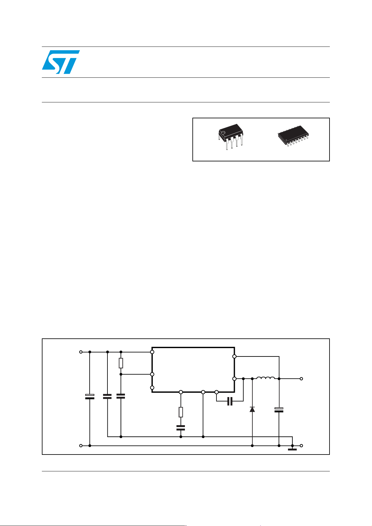
Figure 1. Typical application circuit
L4976
1A step down switching regulator
DIP8 SO16W
Description
The L4976 is a step down monolithic power
switching regulator delivering 1A at a voltage
between 3.3V and 50V (selected by a simple
external divider). Realized in BCD mixed
technology, the device uses an internal power DMOS transistor (with a typical R
obtain very high efficency and high switching
speed. A switching frequency up to 300KHz is
achievable (the maximum power dissipation of the
packages must be observed). A wide input
voltage range between 8V to 55V and output
voltages regulated from 3.3V to 40V cover the
majority of today’s applications. Features of this
new generations of DC-DC converter include
pulse-by-pulse current limit, hiccup mode for short
circuit protection, voltage feedforward regulation,
protection against feedback loop disconnection
and thermal shutdown. The device is available in
plastic dual in line, MINIDIP 8 for standard
assembly, and SO16W for SMD assembly.
ds(ON)
of 0.25Ω) to
Vi=8V to 55V
C
1
220µF
63V
C
7
220nF
R
1
20K
C
2
2.7nF
5
3
2
L4976
7
R
2
9.1K
22nF
1
C
4
6
C
6
100nF
8
4
D1
GI
SB360
L1
260µH
(77120)
C
330µF
VO=3.3V/1A
8
April 2007 Rev 7 1/17
www.st.com
17
Page 2

Contents L4976
Contents
1 Block diagram . . . . . . . . . . . . . . . . . . . . . . . . . . . . . . . . . . . . . . . . . . . . . . 3
2 Pin settings . . . . . . . . . . . . . . . . . . . . . . . . . . . . . . . . . . . . . . . . . . . . . . . . 4
2.1 Pin connection . . . . . . . . . . . . . . . . . . . . . . . . . . . . . . . . . . . . . . . . . . . . . . 4
2.2 Pin description . . . . . . . . . . . . . . . . . . . . . . . . . . . . . . . . . . . . . . . . . . . . . . 4
3 Electrical data . . . . . . . . . . . . . . . . . . . . . . . . . . . . . . . . . . . . . . . . . . . . . . 5
3.1 Maximum ratings . . . . . . . . . . . . . . . . . . . . . . . . . . . . . . . . . . . . . . . . . . . . 5
3.2 Thermal data . . . . . . . . . . . . . . . . . . . . . . . . . . . . . . . . . . . . . . . . . . . . . . . 5
3.3 Operating temperature rating . . . . . . . . . . . . . . . . . . . . . . . . . . . . . . . . . . . 5
4 Electrical characteristics . . . . . . . . . . . . . . . . . . . . . . . . . . . . . . . . . . . . . 7
5 Typical charcteristics . . . . . . . . . . . . . . . . . . . . . . . . . . . . . . . . . . . . . . . . 9
6 Package mechanical data . . . . . . . . . . . . . . . . . . . . . . . . . . . . . . . . . . . . 13
7 Order code . . . . . . . . . . . . . . . . . . . . . . . . . . . . . . . . . . . . . . . . . . . . . . . . 16
8 Revision history . . . . . . . . . . . . . . . . . . . . . . . . . . . . . . . . . . . . . . . . . . . 17
2/17
Page 3

L4976 Block diagram
1 Block diagram
Figure 2. Block diagram
V
CC
5
VOLTAGES
MONITOR
PWM
5.1V
INTERNAL
REFERENCE
3.3V
R
Q
S
DRIVE
CBOOT
CHARGE
CBOOT
CHARGE
AT LIGHT
LOADS
6
BOOT
REF
V
COMP
FB
2
7
8
3.3V
THERMAL
SHUTDOWN
V
REF
E/A
OSCILLATOR
3
OSC GND OUT
1
4
3/17
Page 4

Pin settings L4976
2 Pin settings
2.1 Pin connection
Figure 3. Pin connection (top view)
GND
REF
V
OSC
OUT
1
2
3
4 VCC
DIP8
2.2 Pin description
Table 1. Pin description
N° Pin
DIP8
1 2 GND Ground
2 3 VREF 5.1V Reference voltage with 20mA current capability.
3 4 OSC
SO16W
(1)
N.C.
FB8
COMP
7
BOOT
6
5
Name Description
An external resistor connected between the unregulated
input voltage and this pin and a capacitor connected
from this pin to ground fix the switching frequency. (Line
feed forward is automatically obtained)
GND
REF
V
OSC
OUT
OUT
N.C.
N.C. N.C.
2
3
4
5
6
7
8
SO16
16
15
14
13
12
11
10
N.C.1
N.C.
FB
COMP
BOOT
VCC
N.C.
9
4 5, 6 OUT Stepdown regulator output.
5 11 VCC Unregulated DC input voltage.
6 12 BOOT
7 13 COMP E/A output to be used for frequency compensation.
8 14 FB
1. Pins 1, 7, 8, 9, 10, 15 and 16 are not internally, electrically connected to the die.
4/17
A capacitor connected between this pin and OUT allows
to drive the internal VDMOS.
Stepdown feedback input. Connecting directly to this pin
results in an output voltage of 3.3V. An external resistive
divider is required for higher output voltages.
Page 5

L4976 Electrical data
3 Electrical data
3.1 Maximum ratings
Table 2. Absolute maximum ratings
Symbol
DIP8
V5 V11 Input voltage 58 V
V4 V5, V6
I4 I5, I6 Maximum output current internal limit
V6-V5 V12-V11 14 V
V6 V12 Bootstrap voltage 70 V
S016W
Output DC voltage -1 V
Output peak voltage at t = 0.1µs, f = 200kHz -5 V
Parameter Value Unit
V7 V13
V8 V14
Power dissipation a TA ≤ 60°C
P
TOT
T
J,TSTG
Analogs input voltage (V
(V
= 20V)
CC
Junction and storage temperature
3.2 Thermal data
Table 3. Thermal data
Symbol Parameter
R
thJA
1. Package mounted on board
Maximum thermal resistance junction-ambient
3.3 Operating temperature rating
Table 4. Operating temperature rating
Symbol Parameter
= 24V) 12 V
CC
6 V
-0.3 V
DIP8 1 W
SO16 0.8 W
-40 to 150 °C
DIP8
90
S016W Unit
(1)
110
(1)
Value
°C/W
Unit
T
J
Junction temperature range -40 to 150 °C
5/17
Page 6

Electrical characteristics L4976
4 Electrical characteristics
Table 5. Electrical characteristics
(T
= 25°C, C
J
Symbol Parameter Test condition Min Typ Max Unit
Dynamic characteristic
= 2.7nF, R
OSC
= 20kΩ, VCC = 24V, unless otherwise specified.)
OSC
V
I
V
O
Operating input voltage range
Output voltage
Vd Dropout voltage
Il
Maximum limiting current
Efficiency
fs
Switching frequency
SVRR Supply voltage ripple rejection
Voltage stability of switching
frequency
Temp. stability of switching
frequency
Reference section
Reference voltage 5.0 5.1 5.2 V
Line regulation
Load regulation
Short circuit current 30 65 100 mA
VO = 3.3 to 50V; IO = 1A
IO = 0.5A
I
= 0.2 to 1A
O
+ 2V
ripple
(1)
(1)
; VO = V
RMS
= 100Hz
(1)
V
= 8 to 55V
CC
= 10V; IO = 1A
V
CC
(1)
VCC = 8 to 55V
= 3.3V; IO = 1A
V
O
(1)
VI = V
CC
= 1.A; f
I
O
= 8 to 55V
V
CC
= 0 to 125°C
T
J
I
= 0 to 10mA;
ref
V
= 8 to 55V
CC
I
= 0mA;
ref
V
= 8 to 55V
CC
V
= 0 to 5mA;
ref
V
= 0 to 20mA
CC
(1)
855V
3.33 3.36 3.39 V
3.2923.363.427 V
3.22 3.36 3.5 V
0.29 0.367 V
1.5 2 2.5 A
85 %
90 100 110 KHz
;
ref
60 dB
36%
4%
4.950 5.1 5.250 V
510
210mV
625mV
0.587 V
mV
6/17
Page 7

L4976 Electrical characteristics
Table 5. Electrical characteristics (continued)
(T
= 25°C, C
J
Symbol Parameter Test condition Min Typ Max Unit
DC Characteristics
= 2.7nF, R
OSC
= 20kΩ, VCC = 24V, unless otherwise specified.)
OSC
Iqop
Iq
Total operating quiescent current 4 6 mA
Quiescent current
Error Amplifier
V
FB
R
L
Voltage feedback input 3.33 3.36 3.39 V
Line regulation
Ref. voltage stability vs
temperature
I
O
I
V
oH
V
oL
source
sink
O
Ib
High level output voltage
Low level output voltage
Source output current
Sink output current
Source bias current 2 3 µA
SVRR E/A Supply voltage ripple rejection
DC open loop gain
gm Transconductance
Oscillator section
Duty Cycle = 0; V
= 8 to 55V
V
CC
(1)
= 2.5V
V
FB
= 3.8V
V
FB
= 6V; VFB = 2.5V
V
comp
= 6V; VFB = 3.8V
V
comp
= Vfb; VCC = 8 to 55V
V
comp
R
= ∞
L
I
= -0.1 to 0.1mA
comp
= 6V
V
comp
= 3.8V
FB
2.5 3.5 mA
510mV
0.4
mV/°
10.3 V
0.65 V
180 220 µA
200 300 µA
60 80 dB
50 57 dB
2.5 ms
C
Ramp valley 0.78 0.85 0.92 V
Ramp peak
Maximum duty cycle 95 97 %
Maximum frequency
1. Specification refered to Tj from 0 to 125°C
= 8V
V
CC
V
= 55V
CC
Duty cycle = 0%
R
= 13kW, C
osc
= 820pF
osc
22.152.3 V
9 9.6 10.2 V
300 kHz
7/17
Page 8

Typical charcteristics L4976
5 Typical charcteristics
Figure 4. Quiescent drain current vs.
Iq
(mA)
5
4
3
2
1
input voltage
200KHz
=22K
R
1
=1.2nF
C
2
100KHz
=20K
R
1
=2.7nF
C
2
0Hz
Tamb=25˚C
0% DC
0 5 10 15 20 25 30 35 40 45 50
D97IN724
Vcc(V)
Figure 5. Line regulation
V
O
(V)
3.378
3.376
3.374
3.372
3.370
Tj=125˚C
3.368
3.366
3.364
3.362
3.360
0 0.2 0.4 0.6 0.8 1.0 1.2 1.4 IO(A)
Tj=25˚C
D97IN734
VCC=35V
Figure 6. Quiescent current vs. junction
Iq
(mA)
5
4
3
2
1
-50 -30 -10 10 30 50 70 90 110 Tj(˚C)
temperature
VCC=35V
0% DC
200KHz
R1=22K
C
2
100KHz
R
=20K
1
C2=2.7nF
D97IN731
=1.2nF
0Hz
Figure 7. Switching frquency vs. R1 and
C2
fsw
(KHz)
500
200
0.82nF
1.2nF
100
50
20
2.2nF
3.3nF
4.7nF
5.6nF
10
5
0 20 40 60 80 R1(KΩ)
D97IN784
Tamb=25˚C
8/17
Page 9

L4976 Typical charcteristics
)
Figure 8. Load regulation Figure 9. Switching frequency vs. input
V
O
D97IN733
(V)
3.377
Tj=125˚C
3.376
fsw
(KHz)
107.5
105.0
voltage
D97IN735
3.375
3.374
Tj=25˚C
3.373
3.372
3.371
3.370
0 5 10 15 20 25 30 35 40 45 50 VCC(V)
Figure 10. Switching frequency vs.
fsw
(KHz)
105
100
95
junction temperature
D97IN785
102.5
Tj=25˚C
100.0
97.5
95.0
92.5
90.0
0 5 10 15 20 25 30 35 40 45 50 VCC(V)
Figure 11. Efficiency vs. output current
∆
(V)
0.5
0.4
0.3
0.2
0.1
V
D97IN736
Tj=125˚C
Tj=25˚C
Tj=-25˚C
90
-50 0 50 100 Tj(˚C
Figure 12. Dropout voltage between pin 5
∆
V
(V)
0.5
0.4
0.3
0.2
0.1
0.0
0.0 0.2 0.4 0.6 0.8 1.0 1.2 1.4 IO(A)
and 4
D97IN736
Tj=125˚C
Tj=25˚C
Tj=-25˚C
9/17
0.0
0.0 0.2 0.4 0.6 0.8 1.0 1.2 1.4 IO(A)
Figure 13. Efficiency vs. output current
η
(%)
90
85
VCC=12V
VCC=8V
VCC=24V
80
75
VCC=48V
70
65
60
0 0.2 0.4 0.6 0.8 1.0 1.2 1.4 IO(A)
D97IN739
fsw=100KHz
=3.36V
V
O
Page 10

Typical charcteristics L4976
)
Figure 14. Efficiency vs output voltage Figure 15. Efficiency vs. output current
(%)
96
94
92
90
88
86
84
η
D97IN737
η
(%)
100KHz
200KHz
VCC=35V
IO=1.5A
90
85
80
75
VCC=12V
VCC=24V
VCC=48V
70
65
VCC=8V
fsw=200KHz
=5.1V
V
O
D97IN740
82
0 5 10 15 20 25 VO(V)
Figure 16. Efficiency vs. output current Figure 17. Efficiency vs. Vo
(%)
90
η
VCC=8V
D97IN741
60
0 0.2 0.4 0.6 0.8 1.0 1.2 1.4 IO(A)
Pdiss
(mW)
VCC=35V
fsw=100KHz
800
85
80
VCC=12V
VCC=24V
600
75
70
65
VCC=48V
fsw=200KHz
V
60
55
0.0 0.2 0.4 0.6 0.8 1.0 1.2 1.4 IO(A)
Figure 18. Efficiency vs. V
CC
=3.36V
O
400
200
0
0 5 10 15 20 25 30 V0(V)
Figure 19. Pulse by pulse limiting
current vs. junction
=
2
SW
=100KHz
00KHz
D97IN742
η
(%)
85
80
75
IO=1.5A
V
=5.1V-f
0
V
0
=5.1V-f
V
V
0
=3.36V-f
SW
SW
=3.36V-f
0
SW
=100KHz
=200KHz
Ilim
(A)
2.9
2.8
2.7
2.6
2.5
2.4
temperature.
fsw=100KHz
V
=35V
CC
D97IN744
IO=1.5A
IO=1A
IO=0.5A
D97IN747
70
0 1020304050VCC(V)
10/17
2.3
-50 -25 0 25 50 75 100 125 Tj(˚C
Page 11

L4976 Typical charcteristics
)
Figure 20. Power dissipation vs. V
Pdiss
CC
D97IN743
Figure 21. Load transient
(mW)
VO=5.1V
fsw=100KHz
800
600
IO=1.5A
IO=1A
400
IO=0.5A
200
0
0 1020304050VCC(V)
Figure 22. Line transient Figure 23. Open loop frequency and
V
CC
D97IN786
(V)
30
20
10
V
1
IO = 1A
f
= 100KHz
sw
2
1ms/DIV
O
(mV)
100
0
-100
GAIN
(dB)
50
0
-50
-100
-150
-200
10 10
phase of error amplifier
Phase
10
3
2
10
5
4
10
10
6
GAIN
10
7
D97IN787
8
10
f(Hz
Phase
0
45
90
135
11/17
Page 12

Package mechanical data L4976
6 Package mechanical data
In order to meet environmental requirements, ST offers these devices in ECOPACK®
packages. These packages have a Lead-free second level interconnect . The category of
second level interconnect is marked on the package and on the inner box label, in
compliance with JEDEC Standard JESD97. The maximum ratings related to soldering
conditions are also marked on the inner box label. ECOPACK is an ST trademark.
ECOPACK specifications are available at: www.st.com
12/17
Page 13

L4976 Package mechanical data
Figure 24. DIP8 mechanical data & package dimensions
DIM.
mm inch
MIN. TYP. MAX. MIN. TYP. MAX.
A3.32 0.131
a1 0.51 0.020
B 1.15 1.65 0.045 0.065
b 0.356 0.55 0.014 0.022
b1 0.204 0.304 0.008 0.012
D 10.92 0.430
E 7.95 9.75 0.313 0.384
e2.54 0.100
e3 7.62 0.300
e4 7.62 0.300
F 6.6 0.260
I 5.08 0.200
L 3.18 3.81 0.125 0.150
Z 1.52 0.060
OUTLINE AND
MECHANICAL DATA
DIP-8
13/17
Page 14

Package mechanical data L4976
Figure 25. SO16Wide mechanical data & package dimensions
DIM.
A 2.35 2.65 0.093 0.104
A1 0.10 0.30 0.004 0.012
B 0.33 0.51 0.013 0.200
C 0.23 0.32 0.009 0.013
(1)
D
E 7.40 7.60 0.291 0.299
e 1.27 0.050
H 10.0 10.65 0.394 0.419
h 0.25 0.75 0.010 0.030
L 0.40 1.27 0.016 0.050
k 0˚ (min.), 8˚ (max.)
ddd 0.10 0.004
(1) “D” dimension does not include mold flash , protusions or gate
burrs. Mold flash, p rotusions o r gate bur rs shall not exceed
0.15mm per side.
mm inch
MIN. TYP. MAX. MIN. TYP. MAX.
10.10 10.50 0.398 0.413
OUTLINE AND
MECHANICAL DATA
SO16 (Wide)
14/17
0016021 C
Page 15

L4976 Order code
7 Order code
Table 6. Order code
Part number Package Packaging
L4976 DIP8 Tube
L4976D SO16W Tube
L4976D013TR SO16W Tape and reel
15/17
Page 16

Revision history L4976
8 Revision history
Table 7. Revision history
Date Revision Changes
5-Aug-2001 6 First Issue
3-Apr-2007 7
Document reformatted, updated dropout voltage values in Ta b le 5 o n
page 6
16/17
Page 17

L4976
Please Read Carefully:
Information in this document is provided solely in connection with ST products. STMicroelectronics NV and its subsidiaries (“ST”) reserve the
right to make changes, corrections, modifications or improvements, to this document, and the products and services described herein at any
time, without notice.
All ST products are sold pursuant to ST’s terms and conditions of sale.
Purchasers are solely responsible for the choice, selection and use of the ST products and services described herein, and ST assumes no
liability whatsoever relating to the choice, selection or use of the ST products and services described herein.
No license, express or implied, by estoppel or otherwise, to any intellectual property rights is granted under this document. If any part of this
document refers to any third party products or services it shall not be deemed a license grant by ST for the use of such third party products
or services, or any intellectual property contained therein or considered as a warranty covering the use in any manner whatsoever of such
third party products or services or any intellectual property contained therein.
UNLESS OTHERWISE SET FORTH IN ST’S TERMS AND CONDITIONS OF SALE ST DISCLAIMS ANY EXPRESS OR IMPLIED
WARRANTY WITH RESPECT TO THE USE AND/OR SALE OF ST PRODUCTS INCLUDING WITHOUT LIMITATION IMPLIED
WARRANTIES OF MERCHANTABILITY, FITNESS FOR A PARTICULAR PURPOSE (AND THEIR EQUIVALENTS UNDER THE LAWS
OF ANY JURISDICTION), OR INFRINGEMENT OF ANY PATENT, COPYRIGHT OR OTHER INTELLECTUAL PROPERTY RIGHT.
UNLESS EXPRESSLY APPROVED IN WRITING BY AN AUTHORIZED ST REPRESENTATIVE, ST PRODUCTS ARE NOT
RECOMMENDED, AUTHORIZED OR WARRANTED FOR USE IN MILITARY, AIR CRAFT, SPACE, LIFE SAVING, OR LIFE SUSTAINING
APPLICATIONS, NOR IN PRODUCTS OR SYSTEMS WHERE FAILURE OR MALFUNCTION MAY RESULT IN PERSONAL INJURY,
DEATH, OR SEVERE PROPERTY OR ENVIRONMENTAL DAMAGE. ST PRODUCTS WHICH ARE NOT SPECIFIED AS "AUTOMOTIVE
GRADE" MAY ONLY BE USED IN AUTOMOTIVE APPLICATIONS AT USER’S OWN RISK.
Resale of ST products with provisions different from the statements and/or technical features set forth in this document shall immediately void
any warranty granted by ST for the ST product or service described herein and shall not create or extend in any manner whatsoever, any
liability of ST.
ST and the ST logo are trademarks or registered trademarks of ST in various countries.
Information in this document supersedes and replaces all information previously supplied.
The ST logo is a registered trademark of STMicroelectronics. All other names are the property of their respective owners.
© 2007 STMicroelectronics - All rights reserved
STMicroelectronics group of companies
Australia - Belgium - Brazil - Canada - China - Czech Republic - Finland - France - Germany - Hong Kong - India - Israel - Italy - Japan -
Malaysia - Malta - Morocco - Singapore - Spain - Sweden - Switzerland - United Kingdom - United States of America
www.st.com
17/17
 Loading...