

Page 1
.
3.5AOUTPUTCURRENT
.5.1VTO40VOUTPUTVOLTAGERANGE
.
0 TO 90%DUTY CYCLERANGE
.INTERNALFEED-FORWARD LINE REG.
.INTERNALCURRENTLIMITING
.PRECISE5.1V± 2% ONCHIP REFERENCE
.RESETAND POWERFAILFUNCTIONS
.
INPUT/OUTPUTSYNCPIN
.UNDER VOLTAGE LOCK OUT WITH HYS-
TERETICTURN-ON
.PWM LATCH FOR SINGLE PULSE PER PE-
RIOD
.VERYHIGH EFFICIENCY
.SWITCHING FREQUENCYUP TO 200KHz
.THERMALSHUTDOWN
.CONTINUOUSMODE OPERATION
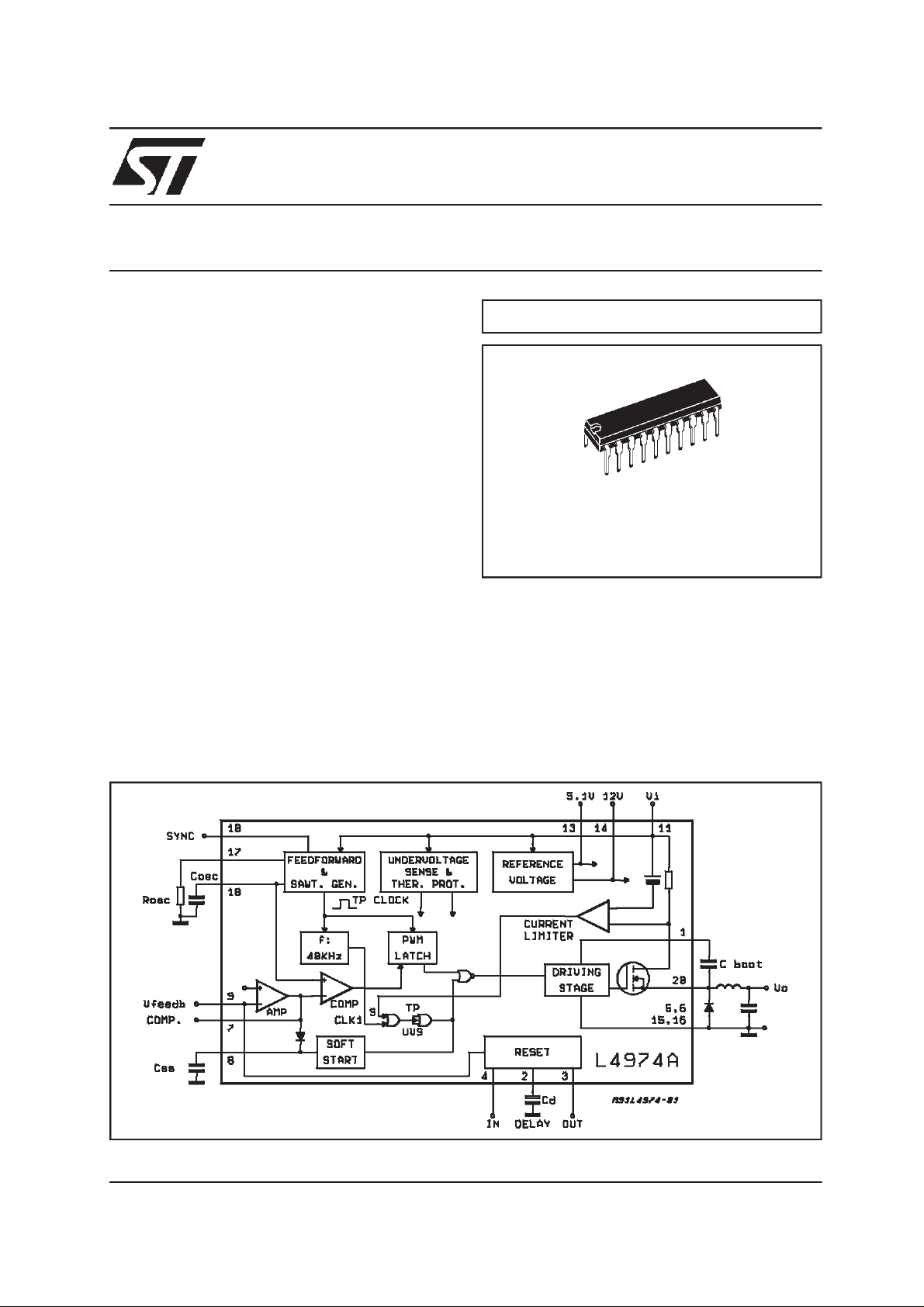
L4974A
3.5ASWITCHINGREGULATOR
MULTIPO WER B CD TECHNOLOGY
POWERDIP (16+2+2)
ORDERINGNUMBER : L4974A
DES CRIPTION
TheL4974Aisa stepdownmonolithicpowerswitching regulator delivering 3.5A at a voltage variable
from5.1to 40V.
Realized with BCD mixed technology, the device
uses a DMOSoutputtransistorto obtainveryhigh
efficiencyandveryfastswitchingtimes.Featuresof
BLOCK DIAGRAM
the L4974A include resetand power fail for microprocessors,feed forwardline regulation,soft start,
limiting current and thermal protection.The device
ismountedin aPowerdip16+2 +2plasticpackage
and requires few external components. Efficient
operation at switching frequencies up to 200KHz
allowsreductioninthesizeandcostof externalfilter
component.
June 2000
This is advanced information on a new product now in development or undergoing evaluation. Details are subject to change without notice.
1/22
Page 2
L4974A
ABSOLU TE MAXIMUM RAT INGS
Symbol Parameter Valu e Unit
V
11
V
11
V
20
I
20
V
I
V
4,V8
V
3
I
3
V
2,V7,V9,V10
I
2
I
7
I
8
P
tot
T
J,Tstg
InputVoltage 55 V
InputOperatingVoltage 50 V
OutputDC Voltage
OutputPeak Voltageat t = 0.1µs f = 200khz
-1
-5
Maximum Output Current Internally Limited
BoostrapVoltage
BoostrapOperating Voltage
65
V
+15
11
InputVoltage at Pins4, 12 12 V
Reset Output Voltage 50 V
Reset Output Sink Current 50 mA
InputVoltage at Pin 2, 7, 9, 10 7 V
Reset Delay Sink Current 30 mA
ErrorAmplifier Output Sink Current 1 A
Soft Start Sink Current 30 mA
TotalPower Dissipation at T
at T
90°C
≤
PINS
=70°C(No copper area on PCB)
amb
5
1.3
Junctionand Storage Temperature -40 to 150 °C
V
V
V
V
W
W
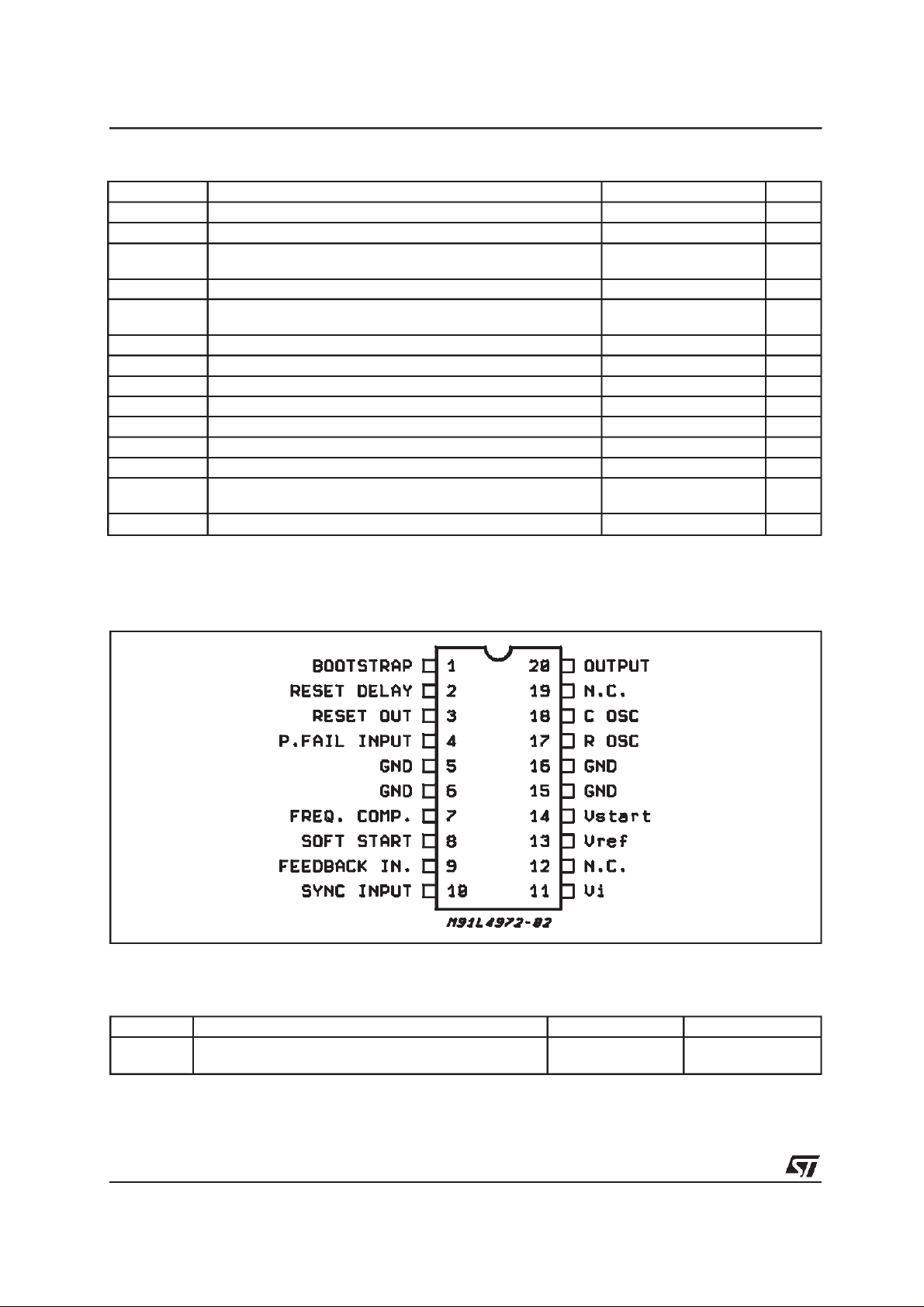
PI N CONNECTION (top view)
THERMAL DATA
Symbol Parame t er Value Uni t
R
th j-pins
R
thj-amb
Thermal ResistanceJunction-Pins max
Thermal ResistanceJunction-ambient max
12
60
°C/W
°C/W
2/22
Page 3
L4974A
PIN FUNCTIONS
o
N
1 BOOTSTRAP A C
2 RESET DELAY A C
3 RESET OUT Open CollectorReset/power Fail Signal Output. This output is high whenthe supply
4 RESET INPUT Input of Power Fail Circuit. The threshold is 5.1V. It may be connected via a divider
5, 6
GROUND Common GroundTerminal
15,16
7 FREQUENCY
COMPENSATION
8 SOFT START Soft StartTime Constant.A capacitoris connectedbetween thi sterminalandground
9 FEEDBACK INPUT The Feedback Terminal of the Regulation Loop.The output is connected directly to
10 SYNC INPUT Multiple L4974A’s are synchronized by connecting pin 10 inputs together or via an
11 SUPPLYVOLTAGE Unregulated InputVoltage.
12,19 N.C. Not Connected.
13 V
14 V
ref
start
17 OSCILLATOR R
18 OSCILLATOR C
20 OUTPUT Regulator Output.
Name Function
capacitor connected between this terminal and the output allows to drive
boot
properlythe internalD-MOS transistor.
capacitor connected between this terminal and ground determines the reset
d
signaldelay time.
and theoutput voltages are safe.
tothe inputforpowerfailfunction.It mustbe connectedtothepin14anexternal30K
resistorwhen power fail signal not required.
A series RC network connected between this terminal and ground determines the
regulation loop gaincharacteristics.
to define the soft start time constant.
thisterminal for5.1V operation; It is connectedvia a dividerfor higher voltages.
externalsyncr. pulse.
5.1VV
DeviceReferenceVoltage.
ref
InternalStart-up Circuit to Drive the PowerStage.
. Externalresistorconnected to grounddeterminestheconstantchargingcurrent
osc
of C
.
osc
. External capacitor connected to ground determines (with R
osc
frequency.
) the switching
osc
Ω
3/22
Page 4

L4974A
CIRCU I T OP ER ATION
The L4974Ais a 3.5Amonolithic stepdownswitchingregulatorworkingincontinuousmoderealizedin
the new BCD Technology. This technologyallows
theintegrationofisolatedverticalDMOSpowertransistorsplusmixed CMOS/Bipolartransistors.
Thedevicecandeliver3.5Aat anoutputvoltageadjustable from 5.1V to 40V and containsdiagnostic
and control functionsthat make it particularly suitable for microprocessorbasedsystems.
BLOCKDIAGRAM
The block diagram shows the DMOSpowertran-
sistorsand the PWM controlloop. Integratedfunctions include a reference voltage trimmed to 5.1V
±2%,softstart,undervoltagelockout,oscillatorwith
feedforward control, pulse by pulse current limit,
thermal shutdown and finally the reset and power
fail circuit.The reset and power failcircuit provides
an outputsignalfora microprocessorindicatingthe
statusof the system.
Deviceturn on is around11V witha typical1V hysterysis,thisthresholdporvidesa correctvoltagefor
the driving stageof the DMOSgateand thehysterysispreventsinstabilities.
Anexternalbootstrapcapacitorchargeto 12Vbyan
internalvoltagereferenceis neededto providecorrect gatedriveto the powerDMOS.Thedrivingcircuit is able to source and sink peak currents of
around0.5A to the gate of the DMOS transistor.A
typical switching time of the current in the DMOS
transistor is 50ns. Due to the fast commutation
switchingfrequenciesup to 200kHzare possible.
The PWMcontrolloopconsistsof a sawtoothoscillator,erroramplifier,comparator,latch andthe outputstage.An errorsignalisproducedby comparing
theoutputvoltagewiththeprecise5.1V±2%onchip
reference.This error signal is then compared with
the sawtooth oscillator in order to generate frixed
frequencypulsewidth modulateddrive for the output stage. A PWM latch is included to eliminate
multiple pulsingwithin a period even in noisy environments.
Thegainand stabilityoftheloopcanbe adjustedby
an externalRC networkconnectedto the outputof
the error amplifier. A voltage feedforward control
has beenaddedto the oscillator,this maintainssuperior line regulation over a wide input voltage
range.Closingthe loopdirectlygivesan outputvoltageof 5.1V,highervoltagesareobtainedbyinserting a voltagedivider.
Atturnon,outputovercurrentsarepreventedbythe
soft start function(fig. 2). The error amplifier is initiallyclampedbyan externalcapacitor,Css,and allowedto riselinearlyunderthe chargeof aninternal
constantcurrentsource.
Outputoverloadprotectionis providedby a current
limitcircuit. Theload currentis sensedby a internal
metalresistorconnectedtoacomparator.Whenthe
loadcurrentexceedsa presetthreshold,the output
of the comparatorsetsa flipflop whichturns offthe
powerDMOS.Thenextclockpulse,fromaninternal
40kHzoscillator,willresettheflipflopandthepower
DMOS will again conduct. This current protection
method,ensuresaconstantcurrentoutputwhenthe
systemis overloadedorshortcircuitedandlimitsthe
switchingfrequency,inthiscondition,to 40kHz.The
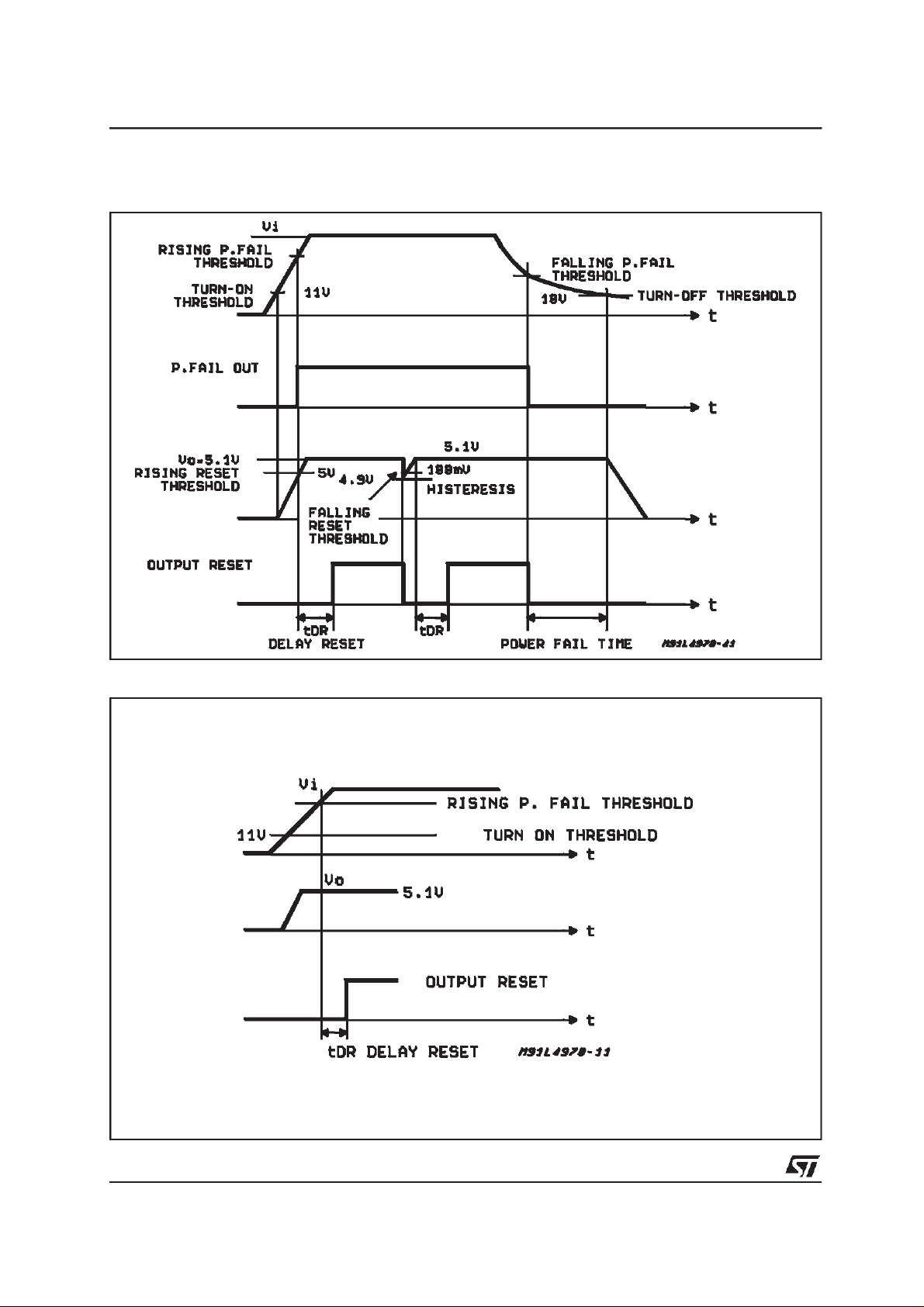
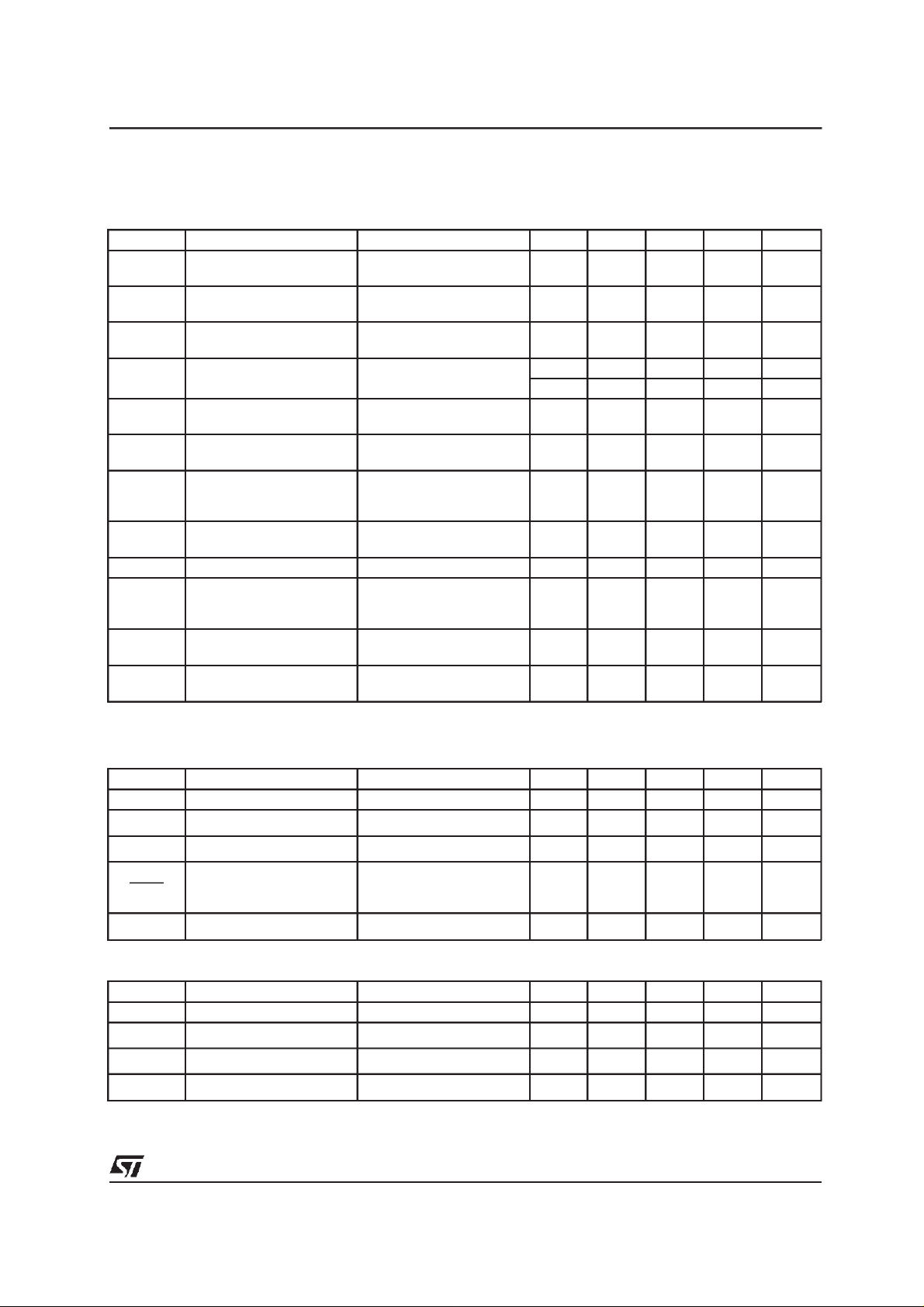
Reset and Power fail circuit (fig. 4), generates an
output signal when the supply voltage exceeds a
threshold programmed by an external voltage divider. The reset signal, is generated with a delay
timeprogrammedbya externalcapacitoronthedelay pin. When the supply voltage falls below the
thresholdor the outputvoltage goes below5V, the
resetoutputgoeslowimmediately.The resetoutput
is an opendrain.
Fig. 4A shows thecasewhen the supplyvoltageis
higherthan the threshold,but the output voltage is
not yet 5V.
Fig.4Bshowsthecasewhentheoutputis5.1V,but
the supply voltage is not yet higher than the fixed
threshold.
The thermal protection disables circuit operation
when the junction temperature reaches about
150°C and has a hysterysis to prevent unstable
conditions.
4/22
Page 5
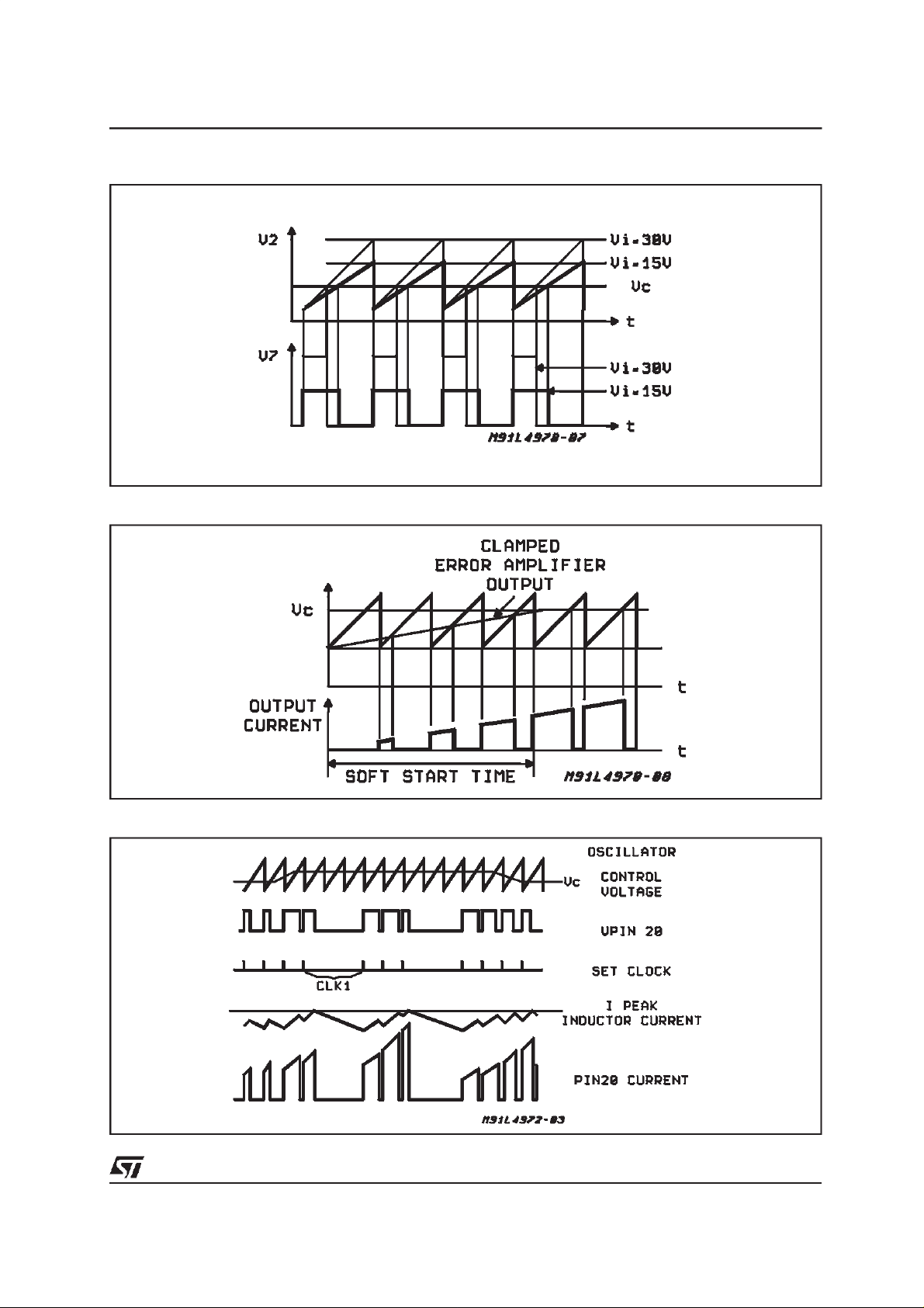
Figure1 : FeedforwardWaveform.
Figure2 : SoftStart Function.
L4974A
Figure3 : LimitingCurrent Function.
5/22
Page 6
L4974A
Figure4 : Resetand PowerFail Functions.
A
B
6/22
Page 7
L4974A
ELECTRICALCHARACTERISTICS (referto the test circuit, TJ=25°C,Vi=35V, R4= 30KΩ,
= 2.7nF,fSW= 100KHztyp, unless otherwisespecified)
C
9
DYNAMICCHARACTERISTICS
Symbol Parameter Test Conditions Min. Typ. Max. Unit Fig.
V
V
∆V
∆V
V
I
20L
InputVolt. Range (pin 11) Vo=V
i
OutputVoltage Vi=15V to 50V
o
Line Regulation VI = 15V to 50V
o
Load Regulation VO =V
o
Dropout Voltage between
d
Pin11 and 20
Max Limiting Current Vi= 15V to 50V
I
o
I
o
I
o
I
o
Io=2A
I
o
V
η
Efficiency I
o
V
Vo= 12V
SVR Supply VoltageRipple
Rejection
V
f = 100Hz; V
f SwitchingFrequency 90 100 110 KHz 5
∆f/∆Vi Voltage Stability of
V
Switching
Frequency
∆f/T
Temperature Stability of
j
Tj=0 to 125°C1%5
SwitchingFrequency
f
max
(*) Pulse testing with a low duty cycle
Maximum Operating
SwitchingFrequency
Vo=V
I
o
ref
to 40V
15 50 V 5
= 3.5A(*)
5 5.1 5.2 V 5
= 2A;Vo=V
ref
12 30 mV
= 1A; Vo=V
refIo
=2Ato3A
= 3.5A
ref
= 1A to 3.5A
825mV
410mV
0.25
0.45
0.4
0.7
V
4 4.75 5.5 A
to 40V
o=Vref
= 3.5A,f = 100KHz
o=Vref
80 85
90
= 2VRMS;Io=5A
i
o=Vref
= 15V to 45V 2 6 % 5
i
= 15KΩ
refR4
56 60 dB 5
200 KHz 5
%
%
= 3.5AC9= 2.2nF
V
SECTION(pin13)
ref
Symbol Parameter Test C o n di tion Mi n . Typ. Max. U n i t Fi g.
ReferenceVoltage 5 5.1 5.2 V 7
Line Regulation Vi= 15V to 50V 10 25 mV 7
13
Load Regulation I13 = 0 to 1mA 20 40 mV 7
13
Average Temperature
13
T
=0°C to 125°C 0.4 mV/°C7
j
Coefficient Reference
∆V
∆V
∆
V
13
V
T
∆
Voltage
V
START
I
13 short
ShortCircuit Current Limit V13= 0 70 mA 7
SECTION(pin15)
Symbol Parameter Test C o n di tion Mi n . Typ. Max. U n i t Fi g.
V
V
∆
V
∆
I
14 short
14
ReferenceVoltage 11.4 12 12.6 V 7
Line Regulation Vi= 15 to 50V 0.6 1.4 V 7
14
Load Regulation I14= 0 to 1mA 50 200 mV 7
14
ShortCircuit Current Limit V15=0V 80 mA 7
7/22
Page 8

L4974A
ELECTRICALCHARACTERISTICS (continued)
DC CHARACTERISTICS
Symbol Parameter Test C o n di tion Mi n . Typ. Max. U n i t F i g .
V
11on
V
11 Hyst
I
11Q
I
11OQ
I
20L
SOFT START(pin8)
Symbol Parameter Test C o n di tion Mi n . Typ. Max. U n i t F i g .
I
8
V
ERRORAMPLIFIER
Symbol Parameter Test C o n di tion Mi n . Typ. Max. U n i t F i g .
V
7H
V
7L
I
7H
-I
7L
I
9
G
SVR Supply VoltageRejection 15 <V
V
OS
RAMP GENERATOR (pin 18)
Turn-onThreshold 10 11 12 V 7A
Turn-offHysteresys 1 V 7A
QuiescentCurrent V8=0; S1=D 13 19 mA 7A
OperatingSupply Current V8= 0; S1 = B; S2 = B 16 23 mA 7A
Out Leak Current Vi= 55V; S3 =A; V8=0 2 mA 7A
SoftStart Source Current V8= 3V; V9= 0V 80 115 150
OutputSaturationVoltage I8 = 20mA; V11= 10V
8
HighLevel Out Voltage I7= -100µA; S1 = C
I
= 200µA; V11= 10V
8
V
= 4.7V
9
6V7C
Low LevelOut Voltage I7 = 100µA; S1 = C
V
= 5.3V;
9
1
0.7
1.2 V 7C
A7B
µ
V
V
SourceOutput Current V7= 1V;V7= 4.7V 100 150 µA7C
SinkOutput Current V7= 6V;V9= 5.3V 100 150
InputBias Current S1 = B; RS= 10K
DC OpenLoop Gain S1 = A; RS=10
V
InputOffset Voltage RS=50
< 50V 60 80 dB 7C
i
Ω
Ω
Ω
S1= A 2 10 mV 7C
0.4 3
60 dB 7C
A7C
µ
A7C
µ
7B
7B
Symbol Parameter Test C o n di tion Mi n . Typ. Max. U n i t F i g .
V
18
V
18
I
18
I
18
Ramp Valley S1 = B; S2 = B 1.2 1.5 V 7A
Ramp Peak S1 = B Vi= 15V
S2 = B V
= 45V
i
Min.Ramp Current S1 = A; I17= 100µA 270 300
2.5
5.5
V
V
A7A
µ
Max. Ramp Current S1 = A; I17 = 1mA 2.4 2.7 mA 7A
SYNCFUNCTION (pin 10)
Symbol Parameter Test C o n di tion Mi n . Typ. Max. U n i t F i g .
8/22
V
10
Low InputVoltage Vi= 15V to 50V;V8=0;
S1 = B; S2 = B; S4 = B
V
10
HighInput voltage V8=0;
S1 = B; S2 = B; S4 = B
+I
10L
+I
10H
SyncInputCurrentwithLow
InputVoltage
Input Current with High
V10=V18= 0.9V; S4 = B;
S1 = B; S2 = B
V10= 2.5V 1.5 mA 7A
InputVoltage
V
10
t
W
OutputAmplitude 4 5 V –
OutputPulse Width V
= 2.5V 0.3 0.5 0.8
thr
–0.3 0.9 V 7A
2.5 5.5 V 7A
0.4 mA 7A
s–
µ
7A
7A
Page 9

L4974A
ELECTR ICAL CHARACTERI STICS (cont inued)
RESETAND POWERFAIL FUNCTIONS
Symbol Parameter Test Conditions Min. Typ. Max. Unit Fig.
V
9R
V
9F
V
2H
V
2L
I
2SO
I
2SI
V
3S
I
3
V
4R
V
4H
I
4
Rising Thereshold Voltage
(pin 9)
Falling TheresholdVoltage
(pin 9)
DelayHigh Threshold Volt. Vi = 15 to 50V
DelayLow Threshold Volt. Vi = 15 to 50V
DelaySource Current V4=5.3V; V2=3V 306080
DelaySource Sink Current V4=4.7V; V2=3V 10 mA 7D
Output SaturationVoltage I3= 15mA;S1 = B V4=4.7V 0.4 V 7D
Output Leak Current V3 = 50V; S1 = A 100
Rising Threshold Voltage V9 = V
Hysteresis 0.4 0.5 0.6 V 7D
InputBias Current 1 3 µA7D
Vi= 15 to 50V
V
= 5.3V
4
Vi = 15 to 50V
V
= 5.3V
4
V
= 5.3V V9=V
4
V
=4.7V V9=V
4
13
V
ref
-130
4.77 Vref
V
ref
-100
-200
V
ref
-80
V
ref
-160
V
mV
V
mV
4.95 5.1 5.25 V 7D
13
1 1.1 1.2 V 7D
13
A7D
µ
A7D
µ
4.955 5.1 5.25 V 7D
7D
7D
Figure5 :
Testand EvaluationBoardCircuit.
TYPICALPERFORMANCES(usingevaluationboard) :
n =83% (V
V
o RIPPLE
Line regulation= 12mV (V
Loadregulation= 8mV(I
= 35V ; Vo=VREF ; Io=3.5A ; fsw= 100KHz)
i
= 30mV(at 1A)
= 15 to 50V)
i
= 1 to 3.5A)
o
for componentvalues Referto thefig. 5 (Partlist).
9/22
Page 10

L4974A
Figure6a : ComponentLayoutof fig.5(1 :1 scale).EvaluationBoard Available
PART LI S T
R1= 30KΩ
R
= 10KΩ
2
R
= 15K
Ω
3
R
= 30K
Ω
4
R
=22
Ω
5
R
= 4.7KΩ
6
R
= see table A
7
R
= OPTION
8
R
= 4.7K
9
*C
** C
* 2 capacitors in parallel to increase input RMS current capability.
* * 3 capacitors in parallel to reduce total output ESR.
Ω
C
3=C4=C5=C6
C
= 390pF Film
7
C
= 22nF MKT 1837(ERO)
8
C
= 2.7nFKP 1830 (ERO)
9
C
= 0.33µFFilm
10
C
= 1nF
11
12=C13=C14
C
=1µF Film
15
= 2,2µF 50V
= 100µF 40V EKR (ROE)
= 1000µF 63V EYF (ROE)
1=C2
D1 = SB 560 (OR EQUIVALENT)
L1 = 150µH
core 58310 MAGNETICS
45 TURNS0.91mm (AWG 19)
COGEMA949181
TableA
V
12V
15V
18V
24V
0
R
9
4.7kΩ
4.7kΩ
4.7k
4.7k
R
6.2kW
9.1kΩ
Ω
Ω
12
18
TableB
SUGGESTEDBOOSTRAPCAPACITORS
Ope ratin g F req u ency Boo st rap Cap . c10
f = 20KHz
f = 50KHz ≥470nF
f =100KHz ≥330nF
f =200KHz
f =500KHz
680nF
≥
220nF
≥
100nF
≥
7
Ω
Ω
10/22
Page 11

Figure 6b: P.C. Board and Component Layout of the Circuit of Fig. 5. (1:1 scale)
L4974A
Figure7 :
DCTest Circuits.
11/22
Page 12

L4974A
Figure7A.
Figure7B.
Figure7C.
12/22
Page 13

Figure7D.
L4974A
Figure8 : QuiescentDrain Currentvs. Supply
Voltage(0% dutycycle - see fig. 7A).
Figure9 : QuiescentDrain Currentvs.Junction
Temperature(0% duty cycle).
13/22
Page 14

L4974A
Figure10 :
Figure12 :
QuiescentDrainCurrent vs. DutyCy-
cle.
ReferenceVoltage(pin 13) vs. Junc-
tionTemperature(see fig. 7).
Figure11 :
Figure13
ReferenceVoltage(pin13) vs.Vi
(seefig. 7).
: ReferenceVoltage(pin14)vs. Vi
(seefig. 7).
Figure14 : ReferenceVoltage(pin 14) vs.Junc-
tionTemperature(see fig. 7).
14/22
Figure15 : ReferenceVoltage5.1V (pin13) Sup-
plyVoltage Ripple Rejectionvs. Fre-
SVR
(dB)
Page 15

L4974A
Figure16 : SwitchingFrequencyvs. InputVoltage
(seefig. 5).
Figure18 : SwitchingFrequencyvs. R4
(seefig.5).
Figure17 : SwitchingFrequencyvs. Junction
Temperature(seefig.5).
Figure19 : MaximumDuty Cyclevs. Frequency.
Figure20 :
SupplyVoltageRippleRejectionvs.
Frequency(see fig.5).
Figure21 :
Efficiencyvs. OutputVoltage.
15/22
Page 16

L4974A
Figure22 :
LineTransientResponse(see fig.5).
Figure24 : DropoutVoltagebetweenPin 11 and
Pin20 vs.Current at Pin20.
Figure23 :
LoadTransientResponse (seefig.5).
Figure25 : .DropoutVoltage betweenPin11 and
Pin20 vs.JunctionTemperature.
Figure26 :
16/22
PowerDissipation(deviceonly) vs.
InputVoltage.
Figure27 :
PowerDissipation (deviceonly) vs.
InputVoltage.
Page 17

L4974A
Figure28 :
Figure30 :
PowerDissipation(deviceonly) vs.
OutputVoltage.
PowerDissipation(deviceonly) vs.
OutputCurrent.
Figure29 :
Figure31
PowerDissipation(device only) vs.
OutputVoltage.
: PowerDissipation(device only)vs.
OutputCurrent.
Figure32 : Efficiencyvs. Output Current. Figure33 : TestPCBThermalCharacteristic.
17/22
Page 18

L4974A
Figure34 : Junctionto AmbientThermalResistance
vs.AreaonBoardHeatsink(DIP16+2+2)
Figure 36: OpenLoop Frequen c yand Phaseof Er-
rorAmplifier(see fig.7C).
Figure 35: Maximum Allowable Power Dissipa-
tion vs. Ambient Temperature (Powerdip)
18/22
Page 19

Figure37 : 3.5A– 5.1VLow CostApplicationCircuit.
L4974A
Figure38 : A 5.1V/12VMultipleSupply.Notethe Synchronizationbetweenthe L4974Aand L4970A.
19/22
Page 20

L4974A
Figure39 : L4974A’sSync.Example.
Figure 40: 1A/24V Multiple Supply. Note the synchronizationbetween the L4974A and L4962
20/22
Page 21

L4974A
DIM.
MIN. TYP. MAX. MIN. TYP. MAX.
a1 0.51 0.020
B 0.85 1.40 0.033 0.055
b 0.50 0.020
b1 0.38 0.50 0.015 0.020
D 24.80 0.976
E 8.80 0.346
e 2.54 0.100
e3 22.86 0.900
F 7.10 0.280
I 5.10 0.201
L 3.30 0.130
Z 1.27 0.050
mm inch
OUTLINE AND
MECHANICAL DATA
Powerdip 20
21/22
Page 22

L4974A
Information furnished is believed to be accurate and reliable. However, STMicroelectronics assumes no responsibility for the consequences of use of such information nor for any infringement of patents or other rights of third parties which may result from its use. No
license is granted by implication or otherwise under any patent or patent rights of STMicroelectronics. Specification mentioned in this
publication are subject to change without notice. This publication supersedes and replaces all information previously supplied. STMicroelectronics products are not authorized for use as critical components in life support devices or systems without express written
approval of STMicroelectronics.
Australia - Brazil - China - Finland - France - Germany - Hong Kong - India - Italy - Japan - Malaysia - Malta - Morocco -
The ST logo is a registered trademark of STMicroelectronics
2000 STMicroelectronics – Printed in Italy – All Rights Reserved
STMicroelectronics GROUP OF COMPANIES
Singapore - Spain - Sweden - Switzerland - United Kingdom - U.S.A.
http://www.st.com
22/22
 Loading...